EP0460429A2 - Verfahren zur Herstellung eines bipolaren Transistors mit einem Heteroübergang - Google Patents
Verfahren zur Herstellung eines bipolaren Transistors mit einem Heteroübergang Download PDFInfo
- Publication number
- EP0460429A2 EP0460429A2 EP91107774A EP91107774A EP0460429A2 EP 0460429 A2 EP0460429 A2 EP 0460429A2 EP 91107774 A EP91107774 A EP 91107774A EP 91107774 A EP91107774 A EP 91107774A EP 0460429 A2 EP0460429 A2 EP 0460429A2
- Authority
- EP
- European Patent Office
- Prior art keywords
- junction region
- covering
- semiconductor
- base layer
- layer
- Prior art date
- Legal status (The legal status is an assumption and is not a legal conclusion. Google has not performed a legal analysis and makes no representation as to the accuracy of the status listed.)
- Withdrawn
Links
Images


Classifications
-
- H—ELECTRICITY
- H10—SEMICONDUCTOR DEVICES; ELECTRIC SOLID-STATE DEVICES NOT OTHERWISE PROVIDED FOR
- H10D—INORGANIC ELECTRIC SEMICONDUCTOR DEVICES
- H10D10/00—Bipolar junction transistors [BJT]
- H10D10/01—Manufacture or treatment
- H10D10/021—Manufacture or treatment of heterojunction BJTs [HBT]
-
- H—ELECTRICITY
- H10—SEMICONDUCTOR DEVICES; ELECTRIC SOLID-STATE DEVICES NOT OTHERWISE PROVIDED FOR
- H10D—INORGANIC ELECTRIC SEMICONDUCTOR DEVICES
- H10D10/00—Bipolar junction transistors [BJT]
- H10D10/80—Heterojunction BJTs
- H10D10/821—Vertical heterojunction BJTs
-
- H—ELECTRICITY
- H10—SEMICONDUCTOR DEVICES; ELECTRIC SOLID-STATE DEVICES NOT OTHERWISE PROVIDED FOR
- H10W—GENERIC PACKAGES, INTERCONNECTIONS, CONNECTORS OR OTHER CONSTRUCTIONAL DETAILS OF DEVICES COVERED BY CLASS H10
- H10W74/00—Encapsulations, e.g. protective coatings
- H10W74/40—Encapsulations, e.g. protective coatings characterised by their materials
-
- H—ELECTRICITY
- H10—SEMICONDUCTOR DEVICES; ELECTRIC SOLID-STATE DEVICES NOT OTHERWISE PROVIDED FOR
- H10D—INORGANIC ELECTRIC SEMICONDUCTOR DEVICES
- H10D62/00—Semiconductor bodies, or regions thereof, of devices having potential barriers
- H10D62/80—Semiconductor bodies, or regions thereof, of devices having potential barriers characterised by the materials
- H10D62/85—Semiconductor bodies, or regions thereof, of devices having potential barriers characterised by the materials being Group III-V materials, e.g. GaAs
-
- H—ELECTRICITY
- H10—SEMICONDUCTOR DEVICES; ELECTRIC SOLID-STATE DEVICES NOT OTHERWISE PROVIDED FOR
- H10P—GENERIC PROCESSES OR APPARATUS FOR THE MANUFACTURE OR TREATMENT OF DEVICES COVERED BY CLASS H10
- H10P14/00—Formation of materials, e.g. in the shape of layers or pillars
- H10P14/60—Formation of materials, e.g. in the shape of layers or pillars of insulating materials
- H10P14/63—Formation of materials, e.g. in the shape of layers or pillars of insulating materials characterised by the formation processes
- H10P14/6326—Deposition processes
- H10P14/6328—Deposition from the gas or vapour phase
- H10P14/6334—Deposition from the gas or vapour phase using decomposition or reaction of gaseous or vapour phase compounds, i.e. chemical vapour deposition
- H10P14/6336—Deposition from the gas or vapour phase using decomposition or reaction of gaseous or vapour phase compounds, i.e. chemical vapour deposition in the presence of a plasma [PECVD]
-
- H—ELECTRICITY
- H10—SEMICONDUCTOR DEVICES; ELECTRIC SOLID-STATE DEVICES NOT OTHERWISE PROVIDED FOR
- H10P—GENERIC PROCESSES OR APPARATUS FOR THE MANUFACTURE OR TREATMENT OF DEVICES COVERED BY CLASS H10
- H10P14/00—Formation of materials, e.g. in the shape of layers or pillars
- H10P14/60—Formation of materials, e.g. in the shape of layers or pillars of insulating materials
- H10P14/69—Inorganic materials
- H10P14/694—Inorganic materials composed of nitrides
- H10P14/6943—Inorganic materials composed of nitrides containing silicon
- H10P14/69433—Inorganic materials composed of nitrides containing silicon the material being a silicon nitride not containing oxygen, e.g. SixNy or SixByNz
Definitions
- the present invention relates to a method of manufacturing a heterojunction bipolar transistor and, more particularly, to a surface passivation technique for an outer periphery of an emitter-base junction or an outer periphery of a collector-base junction.
- a heterojunction bipolar transistor has an ultra-high operation speed and a good current drive capacity compared to a field effect transistor, and thus attracts attention as a device of a new generation.
- An HBT directly uses an epitaxial crystal formed by MBE or MOCVD so that HBT characteristics are fully utilized.
- etching is performed to form a base electrode, and accordingly the outer periphery of the emitter-base junction is exposed.
- the emitter size of an emitter-up HBT or the collector size of a collector-up HBT is decreased.
- surface recombination occurs in the exposed junction, posing a serious problem in decrease in gain. In other words, the higher the value (peripheral length)/(device area), the greater the influence from the surface.
- a collector contact layer 11 consisting of n+-type GaAs
- a collector layer 12 consisting of n-type GaAs
- a base layer 13 consisting of p-type GaAs (first semiconductor)
- an emitter layer 14 consisting of n-type Al 0.3 Ga 0.7 As (second semiconductor)
- an emitter contact layer 15 consisting of n+-type GaAs are sequentially formed on a GaAs substrate 10.
- a upper portion of the base layer 13 and predetermined peripheral regions of the emitter layer 14 and the emitter contact layer 15 are removed by mesa etching to form an HBT mesa structure.
- a upper portion of the collector contact layer 11 and a peripheral region of the collector layer 12 are removed by mesa etching.
- An AuGe/Ni collector electrode 16 is formed on the collector contact layer 11.
- An AuZn/Au base electrode 17 is formed on the base layer 13.
- An AuGe/Ni emitter electrode 18 is formed on the emitter contact layer 15.
- An insulating film 18 of SiO2 or SiN x is deposited on the remaining surface of the HBT not covered by the electrodes.
- an (NH4)2S x treatment is performed immediately after the HBT mesa structure is formed by etching so that S (sulfur) attaches the surface of the structure.
- S-passivation The sulfur or sulfide passivation (S-passivation) mechanism is described in, e.g., a literature "Japanese Journal of Applied Physics", Vol. 28, No. 3, pp. L340 to L342, Mar. 1989.
- S atoms are combined with Ga, Al, and As atoms constituting a semiconductor, thereby saturating the dangling bonds described above.
- the insulating film 19 consisting of SiO2, SiN x , or the like is deposited, and electrodes are formed thereon.
- S-passivation can be performed in accordance with any method as far as S is combined with Ga, Al, As, and the like.
- (NH4)2S is used as a similar compound to (NH4)2S x
- the sulfur content is small and the dangling bonds are not sufficiently saturated.
- Na2S ⁇ 9H2O or the like is used, the device surface might become unstable after the treatment.
- the direction from the emitter to the base of the HBT is preferably set to a ⁇ 011> direction.
- the etching planes become a (111) plane and a ( 11 1) plane or a plane close to this. Since these planes are the planes of III-group Ga and Al, the passivation effect is enhanced by GaS and AlS that are bonded stronger than AsS.
- etching to connect a base electrode is performed by RIE or the like. In this case, wet etching is finally performed to moderate the surface damage. Then, the above-mentioned crystal planes appear in a microscopic manner.
- Sulfur deposited on the surface of the device during S-passivation is amorphous.
- amorphous sulfur sublimes.
- it does not sublime but remains. Therefore, it is preferable that formation of the insulating film 19 after sulfur passivation is performed in accordance with a low-temperature process such as sputtering or ECR-CVD.
- ECR-CVD no damage is caused by plasma and the loss of effect of the S treatment is small compared to the case of plasma process.
- an organic polyimide film or an inorganic SOG film may be formed by wet process.
- the present inventor conducted the following experiments to check effectiveness of this embodiment.
- n+-type GaAs (collector contact layer 11), n-type GaAs (collector layer 12), p-type GaAs (base layer 13), n-type Al 0.3 Ga 0.7 As (emitter layer 14), and n+-type GaAs (emitter contact layer 15) were formed on a GaAs substrate in the same manner as in Fig. 1.
- the n+-type GaAs emitter contact layer was patterned and etched down to the base layer using an H3PO4-based etchant. Subsequently, the base layer was patterned and etched down to the collector contact layer. Similarly, the collector contact layer was patterned and etched down to the substrate.
- the first embodiment relates to an emitter-up HBT.
- the present invention can similarly be applied to a collector-up HBT.
- the dangling bonds are combined with sulfur especially at the exposed portion of the collector-base junction.
- Fig. 2 shows the structure of a collector-up AlGaAs/GaAs HBT.
- both collector electrode 16 and emitter electrode 18 comprise an AuGe/Ni/Ti/Pt/Au structure.
- a base electrode 17 comprises a Ti/Pt/Au structure.
- An insulating film 19 is made of SiN or SiO2 in accordance with ECR-CVD.
- Passivation films were formed in accordance with various methods, e.g., plasma CVD, thermal CVD, and sputtering. The obtained films were compared with a passivation film formed in accordance with ECR-CVD. Thirdly, the effect obtained by performing annealing after formation of the passivation insulating film was studied. An SiN insulating film and an SiO2 insulating film, both of which were formed in accordance with ECR-CVD, were compared to study their effect. These three points will be described.
- the present inventor compared the effects of treatments, performed prior to S-passivation using various types of etchants, by way of a PL (photoluminescence) intensity.
- Fig. 3 shows the obtained results.
- a high PL intensity is obtained at a wavelength corresponding to a band edge.
- a so-called non-isotropical etchant e.g., an ammonium- or sulfuric acid-based etchant
- an opposite mesa etchant refers to an etchant with which the etched surface exhibits an inverted or normal mesa structure.
- a phosphate-based etchant the etched surface exhibits a normal mesa structure in all directions. Therefore, the phosphate-based etchant will be referred to as a isotropic mesa etchant.
- the present inventor compared the PL intensities of respective film deposition methods.
- Fig. 4 shows obtained results.
- a curve a represents a result when an insulating film was formed by ECR-CVD after S-passivation.
- a high PL intensity was obtained at a wavelength corresponding to a band edge.
- a curve b represents a result when S-passivation was performed but an insulating film was not formed.
- Curves c and d represent results when a film was formed by sputtering and thermal CVD, respectively. It is obvious that in these cases the effect of S-passivation was degraded compared to the case of ECR-CVD.
- a curve f represents a result when no treatment was performed.
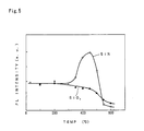
- the present inventor studied the effect of annealing after formation of the insulating film.
- Fig. 5 shows obtained results.
- An SiN film formed in accordance with ECR-CVD exhibits a higher PL intensity when it is annealed at a temperature of 380 to 520°C, and especially 400 to 500°C.
- an SiO2 film is not improved by annealing even when it is formed in accordance with ECR-CVD. Annealing was performed in an nitrogen gas atmosphere for 30 minutes.
- the present inventor fabricated an emitter-up HBT sample to study the effect of the present invention.
- the mesa structure was dipped in a solution of (NH4)2S x for 10 minutes, washed with water for about 20 seconds, and subjected to nitrogen blow to remove water.
- An SiN passivation film was formed on the mesa structure by ECR-CVD and the structure was annealed at 450°C for 30 minutes in a nitrogen gas atmosphere.
Landscapes
- Bipolar Transistors (AREA)
Applications Claiming Priority (4)
| Application Number | Priority Date | Filing Date | Title |
|---|---|---|---|
| JP12389590 | 1990-05-14 | ||
| JP123895/90 | 1990-05-14 | ||
| JP2204530A JPH0472632A (ja) | 1990-05-14 | 1990-08-01 | ヘテロ接合バイポーラトランジスタの製造方法 |
| JP204530/90 | 1990-08-01 |
Publications (2)
| Publication Number | Publication Date |
|---|---|
| EP0460429A2 true EP0460429A2 (de) | 1991-12-11 |
| EP0460429A3 EP0460429A3 (en) | 1993-03-24 |
Family
ID=26460683
Family Applications (1)
| Application Number | Title | Priority Date | Filing Date |
|---|---|---|---|
| EP19910107774 Withdrawn EP0460429A3 (en) | 1990-05-14 | 1991-05-14 | Method of making heterojunction bipolar transistor |
Country Status (2)
| Country | Link |
|---|---|
| EP (1) | EP0460429A3 (de) |
| CA (1) | CA2042467A1 (de) |
Cited By (3)
| Publication number | Priority date | Publication date | Assignee | Title |
|---|---|---|---|---|
| DE4329189A1 (de) * | 1992-09-04 | 1994-03-10 | Tektronix Inc | Verfahren zur implantatfreien Herstellung von aus bipolaren Transistoren mit Heteroübergang bestehenden integrierten Schaltungen |
| EP0671762A3 (de) * | 1994-03-10 | 1997-05-14 | Hughes Aircraft Co | Verringerung der Störkapazität der Basis-Kollektor-Verbindung von bipolaren heterojunktiven Transistoren. |
| US9577070B2 (en) | 2014-11-26 | 2017-02-21 | Taiwan Semiconductor Manufacturing Company, Ltd. | Gate spacers and methods of forming |
Family Cites Families (1)
| Publication number | Priority date | Publication date | Assignee | Title |
|---|---|---|---|---|
| US4920078A (en) * | 1989-06-02 | 1990-04-24 | Bell Communications Research, Inc. | Arsenic sulfide surface passivation of III-V semiconductors |
-
1991
- 1991-05-13 CA CA002042467A patent/CA2042467A1/en not_active Abandoned
- 1991-05-14 EP EP19910107774 patent/EP0460429A3/en not_active Withdrawn
Cited By (6)
| Publication number | Priority date | Publication date | Assignee | Title |
|---|---|---|---|---|
| DE4329189A1 (de) * | 1992-09-04 | 1994-03-10 | Tektronix Inc | Verfahren zur implantatfreien Herstellung von aus bipolaren Transistoren mit Heteroübergang bestehenden integrierten Schaltungen |
| EP0671762A3 (de) * | 1994-03-10 | 1997-05-14 | Hughes Aircraft Co | Verringerung der Störkapazität der Basis-Kollektor-Verbindung von bipolaren heterojunktiven Transistoren. |
| US9577070B2 (en) | 2014-11-26 | 2017-02-21 | Taiwan Semiconductor Manufacturing Company, Ltd. | Gate spacers and methods of forming |
| US10522641B2 (en) | 2014-11-26 | 2019-12-31 | Taiwan Semiconductor Manufacturing Company, Ltd. | Gate spacer and methods of forming |
| US10741662B2 (en) | 2014-11-26 | 2020-08-11 | Taiwan Semiconductor Manufacturing Company, Ltd. | Gate spacer and method of forming |
| US10868129B2 (en) | 2014-11-26 | 2020-12-15 | Taiwan Semiconductor Manufacturing Company, Ltd. | Gate spacer and methods of forming |
Also Published As
| Publication number | Publication date |
|---|---|
| EP0460429A3 (en) | 1993-03-24 |
| CA2042467A1 (en) | 1991-11-15 |
Similar Documents
| Publication | Publication Date | Title |
|---|---|---|
| CA1299982C (en) | Passivation of gallium arsenide electron devices | |
| KR970010738B1 (ko) | 반도체 소자 제조방법 | |
| US4889824A (en) | Method of manufacture semiconductor device of the hetero-junction bipolar transistor type | |
| US5264379A (en) | Method of making a hetero-junction bipolar transistor | |
| EP0460429A2 (de) | Verfahren zur Herstellung eines bipolaren Transistors mit einem Heteroübergang | |
| US5252500A (en) | Method of fabricating a semiconductor device | |
| KR950001145B1 (ko) | 헤테로접합 쌍극성 트랜지스터의 제조방법 | |
| US4981808A (en) | Process for the manufacture of III-V semiconductor devices | |
| JP2817217B2 (ja) | 金属・半導体接合を有する半導体装置およびその製造方法 | |
| JPH0260222B2 (de) | ||
| JP3012071B2 (ja) | 電界効果トランジスタおよびその製造方法 | |
| JP3226666B2 (ja) | 半導体装置の製造方法 | |
| JP3520625B2 (ja) | 半導体装置の製造方法 | |
| JP3055264B2 (ja) | 半導体素子の製造方法 | |
| JPH0249012B2 (de) | ||
| KR940004260B1 (ko) | 갈륨비소 이종접합 트랜지스터의 제조방법 | |
| JPH01144681A (ja) | バイポーラトランジスタの製造方法 | |
| JP2976664B2 (ja) | バイポーラトランジスタの製造方法 | |
| JPS6233741B2 (de) | ||
| JP3222556B2 (ja) | 電極形成方法 | |
| Umebachi et al. | A New Heterojunction-Gate GaAs FET | |
| JP2004260118A (ja) | 半導体装置、半導体装置の製造方法及び半導体装置応用システム | |
| JP2002134525A (ja) | ヘテロ接合バイポーラトランジスタとその製造方法 | |
| JPH04346223A (ja) | オーム性電極の製造方法 | |
| JPH0922892A (ja) | 化合物半導体装置の製造方法 |
Legal Events
| Date | Code | Title | Description |
|---|---|---|---|
| PUAI | Public reference made under article 153(3) epc to a published international application that has entered the european phase |
Free format text: ORIGINAL CODE: 0009012 |
|
| AK | Designated contracting states |
Kind code of ref document: A2 Designated state(s): DE FR GB NL |
|
| PUAL | Search report despatched |
Free format text: ORIGINAL CODE: 0009013 |
|
| AK | Designated contracting states |
Kind code of ref document: A3 Designated state(s): DE FR GB NL |
|
| 17P | Request for examination filed |
Effective date: 19930618 |
|
| 17Q | First examination report despatched |
Effective date: 19941201 |
|
| GRAG | Despatch of communication of intention to grant |
Free format text: ORIGINAL CODE: EPIDOS AGRA |
|
| STAA | Information on the status of an ep patent application or granted ep patent |
Free format text: STATUS: THE APPLICATION HAS BEEN WITHDRAWN |
|
| 18W | Application withdrawn |
Withdrawal date: 19960619 |