EP0460603B1 - Schaltkreis und Verfahren zur Festlegung von Verzögerungsdaten - Google Patents
Schaltkreis und Verfahren zur Festlegung von Verzögerungsdaten Download PDFInfo
- Publication number
- EP0460603B1 EP0460603B1 EP91109108A EP91109108A EP0460603B1 EP 0460603 B1 EP0460603 B1 EP 0460603B1 EP 91109108 A EP91109108 A EP 91109108A EP 91109108 A EP91109108 A EP 91109108A EP 0460603 B1 EP0460603 B1 EP 0460603B1
- Authority
- EP
- European Patent Office
- Prior art keywords
- data
- pin
- pin group
- delay
- delay time
- Prior art date
- Legal status (The legal status is an assumption and is not a legal conclusion. Google has not performed a legal analysis and makes no representation as to the accuracy of the status listed.)
- Expired - Lifetime
Links
- 238000000034 method Methods 0.000 title claims description 13
- 238000012360 testing method Methods 0.000 claims description 27
- 238000012546 transfer Methods 0.000 description 5
- 238000010586 diagram Methods 0.000 description 3
- 230000004044 response Effects 0.000 description 2
- 239000004065 semiconductor Substances 0.000 description 2
- 230000005540 biological transmission Effects 0.000 description 1
- 238000007796 conventional method Methods 0.000 description 1
- 230000007547 defect Effects 0.000 description 1
- 230000002950 deficient Effects 0.000 description 1
- 230000003111 delayed effect Effects 0.000 description 1
- 230000001419 dependent effect Effects 0.000 description 1
- 238000013461 design Methods 0.000 description 1
- 230000006870 function Effects 0.000 description 1
Images


Classifications
-
- G—PHYSICS
- G01—MEASURING; TESTING
- G01R—MEASURING ELECTRIC VARIABLES; MEASURING MAGNETIC VARIABLES
- G01R31/00—Arrangements for testing electric properties; Arrangements for locating electric faults; Arrangements for electrical testing characterised by what is being tested not provided for elsewhere
- G01R31/28—Testing of electronic circuits, e.g. by signal tracer
- G01R31/317—Testing of digital circuits
- G01R31/3181—Functional testing
- G01R31/319—Tester hardware, i.e. output processing circuits
- G01R31/31917—Stimuli generation or application of test patterns to the device under test [DUT]
- G01R31/31922—Timing generation or clock distribution
-
- G—PHYSICS
- G01—MEASURING; TESTING
- G01R—MEASURING ELECTRIC VARIABLES; MEASURING MAGNETIC VARIABLES
- G01R31/00—Arrangements for testing electric properties; Arrangements for locating electric faults; Arrangements for electrical testing characterised by what is being tested not provided for elsewhere
- G01R31/28—Testing of electronic circuits, e.g. by signal tracer
- G01R31/317—Testing of digital circuits
- G01R31/3181—Functional testing
- G01R31/319—Tester hardware, i.e. output processing circuits
- G01R31/31903—Tester hardware, i.e. output processing circuits tester configuration
- G01R31/31908—Tester set-up, e.g. configuring the tester to the device under test [DUT], down loading test patterns
-
- G—PHYSICS
- G01—MEASURING; TESTING
- G01R—MEASURING ELECTRIC VARIABLES; MEASURING MAGNETIC VARIABLES
- G01R31/00—Arrangements for testing electric properties; Arrangements for locating electric faults; Arrangements for electrical testing characterised by what is being tested not provided for elsewhere
- G01R31/28—Testing of electronic circuits, e.g. by signal tracer
- G01R31/317—Testing of digital circuits
- G01R31/3181—Functional testing
- G01R31/319—Tester hardware, i.e. output processing circuits
- G01R31/31903—Tester hardware, i.e. output processing circuits tester configuration
- G01R31/31908—Tester set-up, e.g. configuring the tester to the device under test [DUT], down loading test patterns
- G01R31/3191—Calibration
Definitions
- the present invention relates to a delay data setting circuit and method whereby a delay time for a timing rate pulse of a test clock for each pin of an IC (a semiconductor integrated circuit) is set in a timing generator of an IC tester.
- IC testers have been used for testing ICs to reject defective ICs or to analyze the defects in ICs.
- Such an IC tester generates test pattern data from a pattern generator, based on clocks from a timing generator, derives a signal waveform from pattern data contained in the test pattern data, based on the clocks from the timing generator, and converts the signal waveform into a signal voltage of an ECL or TTL level, which is supplied to corresponding one of pins of an IC under test.
- a response signal voltage obtained at each pin of the IC in this instance is subjected to a logical decision by comparison with a corresponding reference voltage and the logic thus decided is subjected to a logical comparison with expected value pattern data contained in the above-mentioned test pattern data, based on a clock from the timing generator. Thus it is necessary to obtain various test clocks from the timing generator.
- test clock is usually generated, based on a timing rate pulse, and the delay times of circuit elements and transmission lines to the IC tester are not always the same for each pin of the IC under test; therefore, test clocks for respective pins are set so that they are delayed for times ⁇ 1 , ⁇ 2 , ... behind the timing rate pulse, respectively.
- the setting of delay times is performed by a method which sequentially writes pieces of delay time data for respective pins into a delay data memory while sequentially specifying addresses therefor.
- Fig. 1 shows an example of a device which implements the conventional setting method mentioned above.
- the number of pins of an IC (not shown) for which the delay times are to be set is 32 (hereinafter identified by P1, P2, P3, ..., P32) and the delay time data is 32-bit.
- a tester processor 10 and a delay data setting circuit 20, which forms an interface of a timing generator, are interconnected via an 8-bit data bus 30, a clock line 31 and a control line 32, and the delay data setting circuit 20 includes latch circuits 21 and 22, a sequence control circuit 20C and a delay data memory 23.
- the latch circuit 21 is made up of, for example, two 8-bit latches, which fetch data from the data bus 30, based on interface clocks CK1 and CK2, respectively.
- the latch circuit 22 is made up of, for example, four 8-bit latches, which fetch data from the data bus 30, based on interface clocks CK3, CK4, CK5 and CK6, respectively.
- the sequence control circuit 20C responds to a test start signal TS from the tester processor 10 to generate, in synchronization with a tester clock TCK, the interface clocks CK1 through CK6 and a write enable signal WE in a predetermined sequential order at predetermined timing.
- the sequence control circuit 20C responds to the test start signal TS to generate the interface clocks CK1 and CK2 in this order, by which 8-bit address data A1 and A2 from the tester processor 10 are sequentially fetched into the latch circuit 21.
- 8-bit address data A1 and A2 from the tester processor 10 are sequentially fetched into the latch circuit 21.
- predetermined five bits are provided, as address data for the pin P1, to an address terminal ADR of the delay data memory 23.
- the other output bits from the latch circuit 21 are used for the generation of a control signal in the delay data setting circuit 20, but this is a matter of design and hence will not be described.
- delay time data of a total of 32 bits, for the pin P1 is transferred by the interface clocks CK3, CK4, CK5 and CK6, as 8-bit pieces of data D1, D2, D3 and D4 from the tester processor 10 to the latch circuit 22.
- the 32-bit delay time data is supplied to a data input terminal Di of the delay data memory 23.
- the time Tx for the transfer of the address data Al and A2 and the delay time data D1 through D4 from the tester processor 10 to the latch circuit 22 will hereinafter be referred to as a data fetch period.
- the 32-bit delay data for the pin P1 is written into the delay data memory 23 at the address corresponding to the pin P1, by the write enable signal WE which is applied from the sequence control circuit 20C to a write enable terminal WE ⁇ of the delay data memory 23 at predetermined timing.
- the time for this write will hereinafter be referred to as a data write period Ty.
- the tester processor 10 After writing of the data for the pin P1 into the memory 23, the tester processor 10 sends out the address data Al and A2 and the delay time data D1 through D4 for the pin P2, which are fetched into the latch circuits 21 and 22 by the interface clocks CK1 and CK2 and CK3 through CK6, respectively, and the delay time data thus fetched is written by the write enable signal WE into the memory 23 at the address corresponding to the pin P2. Thereafter pieces of delay time data for the pins P3, ... P32 are similarly written into the delay data memory 23 at the addresses corresponding thereto.
- the pieces of delay time data for the pins P1, P2, P3, ..., P32 are read out therefrom at its data output terminal Do, and based on the delay time data, test clocks for the pins P1, P2, P3, ..., P32 are generated.
- the above-described conventional method sequentially writes the pieces of delay time data for respective pins into the delay data memory 23 while sequentially specifying the addresses therefor, and hence takes much time for setting the delay time.
- the time for fetching the address data and the delay time data from the tester processor 10 into the latch circuits 21 and 22 for each pin the time for writing the delay time data into the delay data memory 23 for each pin and the total number of pins for which the delay times are to be set be represented by Tx, Ty and N, respectively, a period of time, N(Tx + Ty), is needed for setting the delay times in the memory 23 for all the pins.
- pins of an IC under test are classified into pin groups according to the delay time to be set for a test clock for each pin, and a table of data, which indicates whether or not each pin belongs to each of the pin groups, is prestored in a pin group table memory. Then, the data indicating whether each pin of each pin groups belongs to the pin group is read out from the pin group table memory for each pin group, and for each pin group, addresses corresponding to the pins belonging to the pin group are sequentially specified by address generating means and the delay time data common to all the pins belonging to the pin group is written into the delay data memory.
- Fig. 3 illustrates in block form an example of a device embodying the setting method of the present invention.
- the total number of pins of an IC for which the afore-mentioned delay time data is to be set is 32 (hereinafter identified by P1, P2, P3, ..., P32) and each delay time data is 32-bit.
- the tester processor 10 and the delay data setting circuit 20 are interconnected via an 8-bit data bus 30, the clock line 31 and the control line 32.
- the delay data setting circuit 20 includes the sequence control circuit 20C, the latch circuits 21 and 22, the delay data memory 23, a pin group table memory 24, a flip-flop group 25 composed of 32 flip-flops, a priority encoder 26, a decoder 27 and a multiplexer 28.
- the multiplexer 28 In the operation for writing the delay time data into the delay time data memory 23 as described below, the multiplexer 28 always responds to a select signal SEL from the sequence control circuit 20C to select and apply the output of the priority encoder 26 to the address terminal ADR of the delay data memory 23.
- the pin group table memory 24 can store a pin group table described later on.
- the flip-flop group 25 is made up of 32 flip-flops.
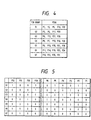
- the delay time of the test clock relative to the timing rate pulse does not always differ with respective pins of the IC, but in practice, there are usually pin groups for each of which the same delay time should be set. This will be described, by way of example, in connection with the case where the same delay time is set for the pins P1, P2, P5, P10 and P32; the same delay time is set for the pins P3, P8, P17 and P29; the same delay time is set for the pins P4, P12, P27 and P28; the same delay time is set for the pins P6, P7, P13, P18 and P30; the same delay time is set for the pins P9, P15, P20, P21 and P26; the same delay time is set for the pins P11, P14, P19, P23 and P24; and the same delay time is set for the pins P16, P22, P25 and P31.
- the relationship between the pin groups and the pins classified by the delay times of the test clocks relative to the timing rate pulse is such
- 32-bit data indicating whether or not each of the pins P1 through P32 belongs to each pin group is produced for each pin group as shown in Fig. 5, and such a pin group data table is loaded in the pin group table memory 24 from the tester processor 10.
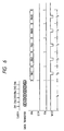
- the sequence therefor is the same as that for the setting of the delay time data described previously in respect of Fig. 1, and hence it will be described with reference to the timing chart of Fig. 2.
- the sequence control circuit 20C When supplied with the test start signal TS from the tester processor 10, the sequence control circuit 20C produces the interface clocks CK1 and CK2 in synchronization with the tester clock TCK and the pieces of address data A1 and A2 which are transferred from the tester processor 10 in 8-bit groups are latched by the clocks CK1 and CK2 in the latch circuit 21. Of a total of 16 bits of the address data, five bits are provided as address data for the pin group G1 to an address terminal ADR of the pin group table memory 24.
- the pieces of data D1 through D4 which are transferred from the tester processor 10 to the latch circuit 22 in 8-bit groups are fetched by the interface clocks CK3, CK4, CK5 and CK6 into the latch circuit 22.
- the pieces of data D1 through D4 of a total of 32 bits indicate whether or not each of the pins P1 through P32 belongs to the pin group G1.
- data "1" in each of the pin groups G1 to G7 indicates that the corresponding pin belongs to the group.
- the 32-bit data is supplied from the latch circuit 22 to a data input terminal Di of the pin group table memory 24, and in response to a write enable signal WE1, the pin group data is written into the address corresponding to the pin group G1.
- 32-bit pin group data indicating whether each of the pins P1 through P32 belongs to each of the pin groups G2, G3, ..., G32 is similarly written into the pin group table memory 24 at the address corresponding to each pin group.
- the pieces of delay time data D1 through D4 of a total of 32 bits common to all of the pins P1, P2, P5, P10 and P32 belonging to the pin group P1, which are transferred from the tester processor 10 in 8-bit groups, are sequentially fetched by the interface clocks CK3, CK4, CK5 and CK6 into the latch circuit 22 in 8-bit groups.
- the delay time data is then supplied to the data input terminal Di of the delay data memory 23.
- the bit position of a "1" which is the least significant in the 32-bit pin group data of the pin group G1 set in the flip-flop group 25 is detected in the priority encoder 26 and 5-bit pin address data PA1 which specifies the pin corresponding to the detected bit position, i.e.
- This 5-bit pin address data PA1 is provided as address data PA to the address terminal ADR of the delay data memory 23 via the multiplexer 28.
- a write enable signal WE2 to the write enable terminal WE ⁇ of the delay data memory 23 from the sequence control circuit 20C, the 32-bit delay time data common to all the pins belonging to the pin group G1 is written into the address PA1 of the delay data memory 23.
- an enable signal EN is applied from the sequence control circuit 20C to the decoder 27, by which the 5-bit address data PA (PA1 in this case) from the priority encoder 26 is decoded into 32-bit data which contains a "1" only at the bit position corresponding to the pin P1 and all "0s” at the other bit positions.
- the priority encoder 26 produces 5-bit pin address data PA2 corresponding to the pin P2 and provides it to the address terminal ADR of the delay data memory 23.
- the write enable signal WE2 is applied again from the sequence control circuit 20C
- the 32-bit delay time data common to the group G1, provided from the latch circuit 22, is written into the memory 23 at the address corresponding to the pin P2.
- pieces of pin address data PA5, PA10 and PA32 are sequentially produced in connection with the other pins P5, P10 and P32 belonging to the pin group G1 and the pieces of delay time data common to the group G1 are sequentially written into the delay data memory 23 at addresses PA5, PA10 and PA32.
- all the bits of the data set in the flip-flop group 25 go to "0s" and then the priority encoder 26 outputs an end signal ES.
- the sequence control circuit 20C Upon receiving the end signal ES, the sequence control circuit 20C transfers it to the tester processor 10.
- the tester processor 10 transfers 16-bit data containing an address specifying the pin group G2, to the latch circuit 21 in 8-bit groups and then transfers 32-bit delay time data common to the pin group G2 to the latch circuit 22 in 8-bit groups.
- the delay time data is written into the delay time data memory 23 at each of the addresses corresponding to the pins P3, P8, P17 and P28 belonging to the pin group G2.
- delay time data common to each of the groups G3, G4, ..., G7 is likewise written into the delay data memory 23 at an address corresponding to each pin belonging to the pin group.
- priority encoder 26 While in the above the priority encoder 26 has been described to detect the bit position of the least significant bit “1" in the 32-bit pin group data, it is evident that the priority encoder 26 may also be used to detect the bit position of the most significant bit "1" in the 32-bit data.
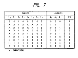
- the priority encoder 26 has such an encoding function as shown in a truth value table of Fig. 7 which shows, for the sake of brevity, the case where it has an 8-bit input and a 3-bit output. In Fig. 7 "X" may assume either a "0" or "1".
- the priority encoder 26 is used to detect the bit position of the most significant bit "1" in this truth value table and encode the bit.
- the output ES of the priority encoder 26 goes to a "1" only when all the input bits are "0s", and this output can be utilized as the end signal ES in Fig. 3.
- a priority encoder is commercially available, for example, as 54F/74F which is an IC by National Semiconductor Inc. and it is easy for those skilled in the art to combine four such ICs to implement the priority encoder with the 32-bit input and the 5-bit output in the Fig. 3 embodiment.
- the time for setting the delay time data for all the pins is 21,500 ns in the above-described embodiment of the invention. Since the time N(Tx + Ty) needed by the conventional setting method described previously with respect to Figs. 1 and 2 is 32,000 ns, the method of the invention affords appreciable reduction of the time. With an increase in the number of pins of an IC, the total number N of pins for which to set the delay time, in practice, is appreciably larger than 32; so that the present invention permits the setting of the delay time in a markedly shorter time than is needed in the prior art.
- the select signal SEL is applied from the sequence control circuit 20C to the multiplexer 28 so that the latter selects the output of the latch circuit 21 -- though this is not related directly to the invention.
- 16-bit data containing address data is provided from the tester processor 10 to the latch circuit 21 in 8-bit groups and five bits of the eight bits are provided as an address to the delay data memory 23 via the multiplexer 28, from which the delay time data for the corresponding pin is read out. By repeating such operations, the delay time data for all the pins is read out.
- the delay time data of the test clock relative to the timing rate pulse for each pin of an IC under test can be set in the timing generator of the IC tester in a short time.
Landscapes
- Engineering & Computer Science (AREA)
- General Engineering & Computer Science (AREA)
- Physics & Mathematics (AREA)
- General Physics & Mathematics (AREA)
- Tests Of Electronic Circuits (AREA)
Claims (6)
- Verfahren des Ladens, von einem Prüfgerätprozessor (10) zum Prüfen von ICs, von Verzögerungszeitdaten, die jedem aus einer Vielzahl von Kontaktstiften eines in Prüfung befindlichen ICs zugeordnet sind, in einen Verzögerungsdatenspeicher (23), wobei die Verzögerungszeitdaten Verzögerungszeiten eines Prüftakts für jeden Kontaktstift repräsentieren, wobei das Verfahren folgende Schritte aufweist:(a) Klassifizieren der Kontaktstifte in eine Mehrzahl von Kontaktstiftgruppen, wobei jede Kontaktstiftgruppe Kontaktstifte enthält, für die die gleichen Verzögerungszeitdaten zu laden sind,(b) Speichern jeweiliger Kontaktstiftgruppendaten für jede der Kontaktstiftgruppen in einen Kontaktstiftgruppentabellenspeicher (24), wobei die Kontaktstiftgruppendaten für jede Kontaktstiftgruppe eine Anzahl an Bits aufweisen, die gleich der Gesamtanzahl an Kontaktstiften ist, wobei jede Bitposition einem jeweiligen der Kontaktstifte zugeordnet ist und entweder einen ersten oder einen zweiten logischen Wert besitzt, der jeweils angibt, ob der zugeordnete Kontaktstift zu der jeweiligen Kontaktstiftgruppe gehört oder nicht,(c) Lesen der einer jeweiligen Kontaktstiftgruppe entsprechenden Kontaktstiftgruppendaten aus dem Kontaktstiftgruppentabellenspeicher,(d) Umwandeln der aus dem Kontaktstiftgruppentabellenspeicher gelesenen Kontaktstiftgruppendaten in eine Sequenz von Adressen des Verzögerungsdatenspeichers, wobei jede Adresse in der Sequenz einem Kontaktstift entspricht, der einer Bitposition zugeordnet ist, welche den ersten logischen Wert besitzt,(e) Anlegen der Sequenz von Adressen, eine nach der anderen, an den Verzögerungsdatenspeicher, während außerdem die zu ladenden Verzögerungszeitdaten für die Kontaktstifte der jeweiligen Kontaktstiftgruppe angelegt werden, wodurch die Verzögerungszeitdaten in den Verzögerungsdatenspeicher sequentiell an den einzelnen Adressen der Sequenz von Adressen geschrieben werden, undsequentielles Ausführen der Schritte (c) bis (e) für jede der Kontaktstiftgruppen.
- Verfahren nach Anspruch 1, bei dem der Schritt (e) des weiteren folgende Schritte aufweist:(e1) Übertragen der zu ladenden Verzögerungszeitdaten für die Kontaktstifte der jeweiligen Kontaktstiftgruppe von dem Prüfgerätprozessor (10) in eine Latch-Einrichtung (22) und Halten der Verzögerungszeitdaten darin, und(e2) Schreiben der in der Latch-Einrichtung (22) gehaltenen Verzögerungszeitdaten sequentiell an den einzelnen Adressen der Sequenz von Adressen des Verzögerungsdatenspeichers (23).
- Verfahren nach Anspruch 1 oder 2, bei dem Schritt (d) des weiteren folgende Schritte aufweist:(d1) Setzen der aus dem Kontaktstiftgruppentabellenspeicher (24) ausgelesenen Kontaktstiftgruppendaten in einer Flipflop-Gruppe (25) derart, daß jedes Flipflop der Flipflop-Gruppe auf den logischen Wert einer jeweiligen der Bitpositionen der Kontaktstiftgruppendaten gesetzt wird,(d2) Bestimmen desjenigen unter den auf den ersten logischen Wert gesetzten Flipflops, welches die Bitposition repräsentiert, die sich auf der höchstwertigen Seite oder niedrigstwertigen Seite der in der Flipflop-Gruppe gesetzten Kontaktstiftgruppendaten befindet, und Erzeugen der Adresse des Kontaktstifts, der der durch das bestimmte Flipflop repräsentierten Bitposition zugeordnet ist,(d3) Schreiben der Verzögerungszeitdaten an die in Schritt (d2) erzeugte Adresse, und dann(d4) Invertieren des logischen Werts des in Schritt (d2) bestimmten Flipflops, und(d5) wiederholtes Ausführen der Schritte (d2) bis (d4), bis Schritt (d2) ergibt, daß kein Flipflop auf den ersten logischen Wert gesetzt ist.
- Schaltung zur Festlegung von Verzögerungsdaten, umfassend:einen Verzögerungsdatenspeicher (23) zum Speichern von Verzögerungszeitdaten für jeden der Kontaktstifte eines in Prüfung befindlichen ICs,einen Kontaktstiftgruppentabellenspeicher (24) zum Speichern jeweiliger Kontaktstiftgruppendaten für jede einer Vielzahl von Kontaktstiftgruppen, wobei die Kontaktstiftgruppendaten für jede Kontaktstiftgruppe eine Anzahl an Bits aufweisen, die der Gesamtanzahl an Kontaktstiften gleich ist, wobei jede Bitposition einem jeweiligen der Kontaktstifte zugeordnet ist und entweder einen ersten oder einen zweiten logischen Wert besitzt, der jeweils angibt, ob der zugeordnete Kontaktstift zu der jeweiligen Kontaktstiftgruppe gehört oder nicht,eine Einrichtung (21, 22) zum Empfangen der Kontaktstiftgruppendaten für jede der Kontaktstiftgruppen von einem Prüfgerätprozessor (10) und zum Speichern der Kontaktstiftgruppendaten in dem Kontaktstiftgruppentabellenspeicher sowie zum Empfangen jeweiliger Verzögerungszeitdaten von dem Prüfgerätprozessor (10) für jede der Gruppen,eine Einrichtung (20C) zum Auslesen, sequentiell für jede Kontaktstiftgruppe, der Kontaktstiftgruppendaten einer jeweiligen Kontaktstiftgruppe aus dem Kontaktstiftgruppentabellenspeicher (24);eine Kontaktstiftadressenerzeugungseinrichtung (25 - 27, 20C) zum sequentiellen Umwandeln der aus dem Kontaktstiftgruppentabellenspeicher (24) ausgelesenen Kontaktstiftgruppendaten in eine Sequenz von Adressen des Verzögerungsdatenspeichers, wobei jede Adresse in der Sequenz einem Kontaktstift entspricht, der einer Bitposition zugeordnet ist, welche den ersten logischen Wert besitzt, undeine Einrichtung (20C) zum Schreiben der gleichen Verzögerungszeitdaten in den Verzögerungsdatenspeicher, sequentiell an jeder Adresse der Sequenz von Adressen.
- Schaltung nach Anspruch 4, bei der die Empfangseinrichtung aufweist:eine erste Latch-Einrichtung (21) zum Abrufen von vom Prüfgerätprozessor (10) übertragenen Adressendaten dorthinein, um Adressen des Kontaktstiftgruppentabellenspeichers (24) zu spezifizieren; undeine zweite Latch-Einrichtung (22) zum Abrufen der vom Prüfgerätprozessor während des Schreibens in den Kontaktstiftgruppentabellenspeicher übertragenen Kontaktstiftgruppendaten dorthinein und zum Abrufen der vom Prüfgerätprozessor während des Schreibens in den Verzögerungsdatenspeicher übertragenen Verzögerungsdaten dorthinein, die den zu einer jeweiligen Kontaktstiftgruppe gehörenden Kontaktstiften gemeinsam sind.
- Schaltung nach Anspruch 4 oder 5, bei der die Kontaktstiftadressenerzeugungseinrichtung aufweist:eine Flipflop-Gruppe (25), die aus einer Vielzahl von Flipflops aufgebaut ist, in denen jeweils logische Werte der jeweiligen Bitpositionen der aus dem Kontaktstiftgruppendatenspeicher (24) ausgelesenen Kontaktstiftgruppendaten gesetzt sind;einen Prioritätscodierer (26), an den die in der Flipflop-Gruppe gesetzten Kontaktstiftgruppendaten geliefert werden und der eine Kontaktstiftadresse eines Kontaktstifts ausgibt, der der Bitposition zugeordnet ist, die den ersten logischen Wert besitzt und sich auf der höchstwertigen Seite oder niedrigstwertigen Seite in den Kontaktstiftgruppendaten befindet; undeine Invertiereinrichtung (27) zum Invertieren des logischen Werts desjenigen der Flipflops der Flipflop-Gruppe (25), der der aus dem Prioritätscodierer ausgegebenen Kontaktstiftadresse entspricht.
Applications Claiming Priority (2)
| Application Number | Priority Date | Filing Date | Title |
|---|---|---|---|
| JP150339/90 | 1990-06-08 | ||
| JP2150339A JP2813237B2 (ja) | 1990-06-08 | 1990-06-08 | Ic試験用クロック遅延時間の設定方法 |
Publications (3)
| Publication Number | Publication Date |
|---|---|
| EP0460603A2 EP0460603A2 (de) | 1991-12-11 |
| EP0460603A3 EP0460603A3 (en) | 1992-07-01 |
| EP0460603B1 true EP0460603B1 (de) | 1997-04-23 |
Family
ID=15494840
Family Applications (1)
| Application Number | Title | Priority Date | Filing Date |
|---|---|---|---|
| EP91109108A Expired - Lifetime EP0460603B1 (de) | 1990-06-08 | 1991-06-04 | Schaltkreis und Verfahren zur Festlegung von Verzögerungsdaten |
Country Status (5)
| Country | Link |
|---|---|
| US (1) | US5305329A (de) |
| EP (1) | EP0460603B1 (de) |
| JP (1) | JP2813237B2 (de) |
| KR (1) | KR960000615B1 (de) |
| DE (1) | DE69125751T2 (de) |
Families Citing this family (7)
| Publication number | Priority date | Publication date | Assignee | Title |
|---|---|---|---|---|
| US5365528A (en) * | 1992-04-03 | 1994-11-15 | At&T Bell Laboratories | Method for testing delay faults in non-scan sequential circuits |
| JP3192278B2 (ja) * | 1993-06-10 | 2001-07-23 | 富士通株式会社 | プリント板配線試験処理方法 |
| US5544175A (en) * | 1994-03-15 | 1996-08-06 | Hewlett-Packard Company | Method and apparatus for the capturing and characterization of high-speed digital information |
| JP2889113B2 (ja) * | 1994-04-26 | 1999-05-10 | インターナショナル・ビジネス・マシーンズ・コーポレイション | 遅延発生装置、デ−タ処理システム及びデ−タ伝送システム |
| TW343282B (en) * | 1996-06-14 | 1998-10-21 | Adoban Tesuto Kk | Testing device for a semiconductor device |
| JPH10170603A (ja) * | 1996-12-13 | 1998-06-26 | Ando Electric Co Ltd | Icテスタのキャリブレーション方法 |
| EP1085335A1 (de) | 1999-09-14 | 2001-03-21 | Alcatel | Verfahren und Vorrichtung zum Testen integrierter Schaltungen mit einer automatischen Testeinrichtung |
Family Cites Families (5)
| Publication number | Priority date | Publication date | Assignee | Title |
|---|---|---|---|---|
| US4493079A (en) * | 1982-08-18 | 1985-01-08 | Fairchild Camera & Instrument Corp. | Method and system for selectively loading test data into test data storage means of automatic digital test equipment |
| DE3237365A1 (de) * | 1982-10-08 | 1984-04-12 | Siemens AG, 1000 Berlin und 8000 München | Anordnung zur erzeugung von mustern von pruefsignalen bei einem pruefgeraet |
| JPS6089773A (ja) * | 1983-08-01 | 1985-05-20 | フエアチアイルド カメラ アンド インストルメント コ−ポレ−シヨン | 自動テスト方式における信号のタイミングを動的に制御する方法及び装置 |
| US4730318A (en) * | 1986-11-24 | 1988-03-08 | International Business Machines Corporation | Modular organized storage tester |
| US4837521A (en) * | 1987-07-02 | 1989-06-06 | Schlumberger Systems & Services, Inc. | Delay line control system for automatic test equipment |
-
1990
- 1990-06-08 JP JP2150339A patent/JP2813237B2/ja not_active Expired - Fee Related
-
1991
- 1991-05-31 US US07/713,996 patent/US5305329A/en not_active Expired - Lifetime
- 1991-06-04 DE DE69125751T patent/DE69125751T2/de not_active Expired - Fee Related
- 1991-06-04 EP EP91109108A patent/EP0460603B1/de not_active Expired - Lifetime
- 1991-06-08 KR KR1019910009454A patent/KR960000615B1/ko not_active Expired - Fee Related
Also Published As
| Publication number | Publication date |
|---|---|
| US5305329A (en) | 1994-04-19 |
| KR960000615B1 (ko) | 1996-01-10 |
| DE69125751T2 (de) | 1997-09-18 |
| EP0460603A3 (en) | 1992-07-01 |
| EP0460603A2 (de) | 1991-12-11 |
| JPH0442072A (ja) | 1992-02-12 |
| DE69125751D1 (de) | 1997-05-28 |
| JP2813237B2 (ja) | 1998-10-22 |
Similar Documents
| Publication | Publication Date | Title |
|---|---|---|
| EP0023419B1 (de) | Verfahren und Vorrichtung zum Testen einer logischen Schaltung | |
| JPS63182585A (ja) | テスト容易化機能を備えた論理回路 | |
| US5155732A (en) | Method and apparatus for data transfer to and from devices through a boundary-scan test access port | |
| JPS6231439B2 (de) | ||
| US5412662A (en) | Memory testing device for preventing excessive write and erasure | |
| US4670879A (en) | Pattern generator | |
| US5581564A (en) | Diagnostic circuit | |
| EP0460603B1 (de) | Schaltkreis und Verfahren zur Festlegung von Verzögerungsdaten | |
| US4312067A (en) | Function test evaluation apparatus for evaluating a function test of a logic circuit | |
| EP0632387A2 (de) | Verfahren und Gerät zur Einfügung der Zustände nicht-abtastbarer Teile in einer Abtastkette | |
| US4819166A (en) | Multimode scan apparatus | |
| US6141782A (en) | Pseudo-scan testing using hardware-accessible IC structures | |
| JP3102600B2 (ja) | Icテスタ | |
| KR0143131B1 (ko) | 램 테스트를 위한 최적 데이타 발생기 | |
| GB2175097A (en) | Testing digital integrated circuits | |
| EP0157036A2 (de) | Serienchipabtastung | |
| JPH0526979A (ja) | テスト容易化回路 | |
| JPH06302199A (ja) | メモリテスト回路装置 | |
| JPH06295597A (ja) | メモリテスト回路装置 | |
| JP2001195894A (ja) | 外付け半導体メモリ試験装置 | |
| EP0825614A2 (de) | Vorrichtung und Verfahren zur Messung der Geschwindigkeit einer Speichereinheit in einer integrierten Schaltung | |
| JPS6310458B2 (de) | ||
| JPH06148291A (ja) | バウンダリスキャンレジスタ | |
| JPH02298877A (ja) | 集積回路の自動テスト回路生成方法 | |
| KR19990036160U (ko) | 블랙리스트검사장치 |
Legal Events
| Date | Code | Title | Description |
|---|---|---|---|
| PUAI | Public reference made under article 153(3) epc to a published international application that has entered the european phase |
Free format text: ORIGINAL CODE: 0009012 |
|
| 17P | Request for examination filed |
Effective date: 19910604 |
|
| AK | Designated contracting states |
Kind code of ref document: A2 Designated state(s): DE FR NL |
|
| PUAL | Search report despatched |
Free format text: ORIGINAL CODE: 0009013 |
|
| AK | Designated contracting states |
Kind code of ref document: A3 Designated state(s): DE FR NL |
|
| 17Q | First examination report despatched |
Effective date: 19950721 |
|
| GRAG | Despatch of communication of intention to grant |
Free format text: ORIGINAL CODE: EPIDOS AGRA |
|
| GRAH | Despatch of communication of intention to grant a patent |
Free format text: ORIGINAL CODE: EPIDOS IGRA |
|
| RBV | Designated contracting states (corrected) |
Designated state(s): DE |
|
| GRAH | Despatch of communication of intention to grant a patent |
Free format text: ORIGINAL CODE: EPIDOS IGRA |
|
| GRAA | (expected) grant |
Free format text: ORIGINAL CODE: 0009210 |
|
| AK | Designated contracting states |
Kind code of ref document: B1 Designated state(s): DE |
|
| REF | Corresponds to: |
Ref document number: 69125751 Country of ref document: DE Date of ref document: 19970528 |
|
| PLBE | No opposition filed within time limit |
Free format text: ORIGINAL CODE: 0009261 |
|
| STAA | Information on the status of an ep patent application or granted ep patent |
Free format text: STATUS: NO OPPOSITION FILED WITHIN TIME LIMIT |
|
| 26N | No opposition filed | ||
| PGFP | Annual fee paid to national office [announced via postgrant information from national office to epo] |
Ref country code: DE Payment date: 19990628 Year of fee payment: 9 |
|
| PG25 | Lapsed in a contracting state [announced via postgrant information from national office to epo] |
Ref country code: DE Free format text: LAPSE BECAUSE OF NON-PAYMENT OF DUE FEES Effective date: 20010403 |