EP0460660B1 - Einrichtung zur Ansteuerung eines piezoelektrischen Elements - Google Patents
Einrichtung zur Ansteuerung eines piezoelektrischen Elements Download PDFInfo
- Publication number
- EP0460660B1 EP0460660B1 EP91109273A EP91109273A EP0460660B1 EP 0460660 B1 EP0460660 B1 EP 0460660B1 EP 91109273 A EP91109273 A EP 91109273A EP 91109273 A EP91109273 A EP 91109273A EP 0460660 B1 EP0460660 B1 EP 0460660B1
- Authority
- EP
- European Patent Office
- Prior art keywords
- piezoelectric element
- switching means
- discharging
- turned
- voltage
- Prior art date
- Legal status (The legal status is an assumption and is not a legal conclusion. Google has not performed a legal analysis and makes no representation as to the accuracy of the status listed.)
- Expired - Lifetime
Links
- 238000007599 discharging Methods 0.000 claims description 133
- 238000002347 injection Methods 0.000 description 22
- 239000007924 injection Substances 0.000 description 22
- 239000000446 fuel Substances 0.000 description 20
- 238000010586 diagram Methods 0.000 description 6
- 230000010287 polarization Effects 0.000 description 2
- 230000006835 compression Effects 0.000 description 1
- 238000007906 compression Methods 0.000 description 1
- 230000004048 modification Effects 0.000 description 1
- 238000012986 modification Methods 0.000 description 1
Images




Classifications
-
- F—MECHANICAL ENGINEERING; LIGHTING; HEATING; WEAPONS; BLASTING
- F02—COMBUSTION ENGINES; HOT-GAS OR COMBUSTION-PRODUCT ENGINE PLANTS
- F02D—CONTROLLING COMBUSTION ENGINES
- F02D41/00—Electrical control of supply of combustible mixture or its constituents
- F02D41/20—Output circuits, e.g. for controlling currents in command coils
- F02D41/2096—Output circuits, e.g. for controlling currents in command coils for controlling piezoelectric injectors
-
- H—ELECTRICITY
- H10—SEMICONDUCTOR DEVICES; ELECTRIC SOLID-STATE DEVICES NOT OTHERWISE PROVIDED FOR
- H10N—ELECTRIC SOLID-STATE DEVICES NOT OTHERWISE PROVIDED FOR
- H10N30/00—Piezoelectric or electrostrictive devices
- H10N30/80—Constructional details
- H10N30/802—Circuitry or processes for operating piezoelectric or electrostrictive devices not otherwise provided for, e.g. drive circuits
Definitions
- the present invention relates to a device for driving a piezoelectric element.
- a well known device for charging and discharging a piezoelectric element is adapted to charge an electric charge to a power condenser of a piezoelectric element through a charging coil, and discharge the electric charge in the piezoelectric element through a discharging coil, but this device has a problem such that the discharged electric charge is wastefully consumed.
- a device for charging and discharging a piezoelectric element in which a part of the discharged electric charge is recovered by a power condenser, to reduce the power consumption (refer to Japanese utility model publication No. 62-117251).
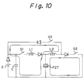
- the above device for charging and discharging a piezoelectric element in principle, comprises a first discharging circuit for discharging an electric charge in a piezoelectric element PZT to the ground through a discharging coil L2, and a second discharging circuit for discharging an electric charge in the piezoelectric element PZT to a high potential side of a power condenser C, through the discharging coil L2, as shown in Fig. 10.
- the power condenser C is charged by a high voltage generator E, and when a switching means S1 is turned ON, the electric charge in the power condenser C is charged to the piezoelectric element PZT through a charging coil L1.
- a switching means S3 is initially turned ON and the electric charge in the piezoelectric element PZT is discharged through the second discharging circuit, so that the discharged electric charge is recovered by the power condenser C. Then, the switching means S3 is turned OFF and a switching means S2 is turned ON, so that the electric charge in the piezoelectric element PZT is discharged through the first discharging circuit. Accordingly, since the power condenser C is thus charged not only by the high voltage generator E but also by the discharged electric charge, the power consumption can be reduced.
- the terminal voltage of the piezoelectric element PZT during the discharging operation becomes a high negative voltage
- the polarization state of the piezoelectric element PZT is changed, the amount of expansion of the piezoelectric element is reduced, and the piezoelectric element is heated whereby the polarization becomes poor. Therefore, it is necessary to control the terminal voltage of the piezoelectric element PZT during the discharging operation so that a high negative voltage does not occur.
- the amount of expansion of the piezoelectric element PZT can be controlled by the terminal voltage of the piezoelectric element PZT during the discharging operation, preferably the terminal voltage of the piezoelectric element PZT is freely set during the discharging operation.
- the device for charging and discharging a piezoelectric element as disclosed in the above Japanese Unexamined Utility Model Publication No. 62-117251 can to a certain extent prevent the terminal voltage of the piezoelectric element PZT from becoming a negative voltage during a discharging operation, it cannot completely prevent this phenomenon. Namely this device has less control of the terminal voltage of the piezoelectric element, during the discharging operation, to thus obtain a predetermined positive voltage. This problem will be further discussed with reference to Fig. 10 and Figs. 11(A) to 11(F).
- the electrostatic capacity of the power condenser C is much larger than that of the piezoelectric element PZT, and the high voltage generator E generates a voltage as high as 320 (V).
- the terminal voltage of a high potential side of the power condenser C is, therefore, substantially 320 (V), and when the switching means S1 is turned ON in this state, the piezoelectric element PZT is charged and the terminal voltage of the piezoelectric element PZT becomes as high as 600 (V).
- the switching element S3 is initially turned ON, and then the switching element S2 is turned ON, and thereafter, a discharging operation is started.
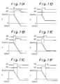
- the change of the terminal voltage of the piezoelectric element PZT at this time is shown in Figs. 11(A), 11(B) and 11(C).
- Fig. 11(A) shows a state wherein the switching element S3 is turned ON for a short time.
- the switching element S3 is turned on, the electric charge in the piezoelectric element PZT is recovered by the power condenser C through the second discharging circuit, but since the switching means S3 is turned ON for only a short time, there is little drop in the terminal voltage V of the piezoelectric element PZT during this time.
- the switching means S3 is turned OFF and the switching means S2 is turned ON, the electric charge in the piezoelectric element PZT is discharged through the first discharging circuit, and since the piezoelectric element PZT and the discharging coil L2 constitute a resonance circuit at this time, the terminal voltage V of the piezoelectric element PZT after the discharging operation is completed becomes a negative voltage.
- the magnitude of the negative voltage is almost 1/3 of the terminal voltage V (positive voltage) of the piezoelectric element PZT when the switching means S2 is turned ON and the discharging operation is started in the first discharging circuit. Namely, as exemplified in Fig.
- Fig. 11(B) shows an example wherein the switching means S3 is turned ON for a longer time, i.e., where the switching means S3 is turned OFF and the switching means S2 is turned ON when the terminal voltage V of the piezoelectric element PZT drops to as low as 400 (V).
- the negative voltage generated in the terminal of the piezoelectric element PZT after the discharging operation is completed is slightly lower, at approximately - 150 (V).
- Fig. 11(C) shows an example wherein the switching means S3 is turned ON until the discharging operation through the second discharging circuit is completed, and thereafter, the switching means S2 is turned ON.
- the switching means S3 is turned ON, the piezoelectric element PZT, the power condenser C and the discharging coil L2 constitute a resonance circuit, and at this time, the terminal voltage of the piezoelectric element PZT after the discharging operation is completed is also lower by about 1/3 of the terminal voltage V of the piezoelectric element PZT when the discharging operation is started, where the terminal voltage (approximately 320 (V)) of a high potential side of the power condenser C is taken as a reference, than the terminal voltage of a high potential side of the power condenser C.
- V terminal voltage
- the terminal voltage V of the piezoelectric element PZT where the terminal voltage of a high potential side of the power condenser C when the discharging operation is started is regarded as a reference is approximately 300 (V)
- the terminal voltage V of the piezoelectric element PZT after the discharging operation is completed becomes approximately 200 (V)
- the switching means S2 is not turned ON, the terminal voltage V of the piezoelectric element PZT is maintained at approximately 200 (V).
- Fig. 11(C) shows an example wherein the switching means S2 is turned ON when the terminal voltage V of the piezoelectric element falls to approximately 200 (V).
- the negative voltage generated in the terminal of the piezoelectric element PZT after the discharging operation is finished becomes approximately 1/3 of the terminal voltage V of the piezoelectric element PZT at the time of the start of the discharging operation, and therefore, the negative voltage generated at the terminal of the piezoelectric element PZT after the completion of the discharging operation is as low as - 80 V.
- the switching means S2 is turned OFF before the discharging operation is completed, i.e., if the ON time of the switching means S2 is short, energy stored in the discharging coil L2 is abruptly discharged when the switching means S2 is turned OFF, and thus the switching means S2 is damaged.
- the switching means S2 cannot be, thus turned OFF until the discharging operation is completed, and thus the terminal voltage V of the piezoelectric element PZT after the discharging operation is completed becomes approximately - 80 (V). Accordingly, if the electric charge charged in the piezoelectric element PZT is discharged through the second discharging circuit, and then discharged through the first discharging circuit, the terminal voltage V of piezoelectric element PZT after the completion of the discharging operation cannot be maintained at a negative voltage lower than approximately - 80 (V), and further, cannot be maintained at a constant positive voltage.
- the terminal voltage V of the piezoelectric element PZT can be set at any voltage between - 200 (V) and + 200 (V).
- the switching means S2 is turned ON, the discharge of the electric charge in the piezoelectric element PZT is started through the first discharging circuit, and therefore, the terminal voltage V of the piezoelectric element PZT begins to drop.
- the switching means S2 is turned OFF and the switching means S3 is turned ON, the discharging operation is started through the second discharging circuit.
- the piezoelectric element PZT When the switching means S2 is turned ON and the discharge of the electric charge in the piezoelectric element PZT is started, the piezoelectric element PZT continues to emit energy and the terminal voltage V of the piezoelectric element PZT continues to fall.
- the piezoelectric element PZT begins to emit energy, a current is to flow caused continuously through the discharging coil L2 in the direction shown by arrows indicating the first discharging circuit, and this energy is gradually accumulated in the discharging coil L2. Then, when the switching means S2 is turned OFF and the switching means S3 is turned ON, the energy accumulated in the discharging coil L2 is applied to the power condenser C via the second discharging circuit, and thus the power condenser C is charged.
- the terminal voltage V of the piezoelectric element PZT continuous to fall. Then, when the flow of current through the discharging coil L2 is stopped, i.e., when the discharging operation is completed, the terminal voltage V of the piezoelectric element PZT becomes a constant voltage. Namely, as shown in Fig.
- the terminal voltage V of the piezoelectric element PZT when the discharging operation is completed is changed in accordance with the ON time of the switching means S2; the longer the ON time of the switching means S2, the lower the terminal voltage V of the piezoelectric element PZT.
- the terminal voltage V of the piezoelectric element PZT, after the discharging operation is completed can be changed within a range of from - 200 (V) to + 200 (V) by changing the ON time of the switching means S2.
- An object of the present invention is to provide a device for driving a piezoelectric element in which the terminal voltage of the piezoelectric element can be changed over a wide range after a discharging operation is completed.
- a device for driving a piezoelectric element comprising: a power condenser having a high voltage side terminal; first switching means connected between the piezoelectric element and the high voltage side terminal of the power condenser for charging the piezoelectric element by using a high potential at the high voltage side terminal of the power condenser; a first discharging circuit having a discharging coil therein and connected between the piezoelectric element and the ground for discharging the piezoelectric element to the ground via the first discharging circuit; a second discharging circuit having a discharging coil therein and connected between the piezoelectric element and the high voltage side terminal of the power condenser for discharging the piezoelectric element to the high voltage side terminal of the power condenser via the second discharging circuit; and discharge control means for discharging the piezoelectric element to the high voltage side terminal of the power condenser via the second discharging circuit after discharging the piezoelectric element to
- the present invention will be described by exemplifying a device for driving a piezoelectric element for controlling fuel injection.
- a fuel injection valve 1 comprises a needle 4 sliding inserted into a housing 2, to control the opening and closing of a nozzle port 3, a needle pressuring chamber 6 formed on the circumference of a conical pressure receiving face 5 of the needle 4, a piston 7 slidingly inserted into the housing 2, a piezoelectric element PZT inserted between the housing 2 and the piston 7, a disk spring 8 biasing the piston 7 toward the piezoelectric element PZT, a pressure control chamber 9 formed between the needle 4 and the piston 7, and a compression spring 10 biasing the needle 4 toward the nozzle port 3.
- the pressure control chamber 9 is connected to the needle pressuring chamber 6 through a restriction passage 11 formed on the circumference of the needle 4, and the needle pressurizing chamber 6 is connected to an accumulator 14 filled with high pressure fuel through a fuel passage 12 and a fuel distribution pipe 13.
- the high pressure fuel in the accumulator 14 is conducted to the needle pressurizing chamber 6, and a part of the high pressure fuel is fed to the pressure control chamber 9 through the restriction passage 11, and thus the fuel pressure in the needle pressurizing chamber 6 and the pressure control chamber 9 is substantially equal to the high pressure in the accumulator 14.
- the piston is lowered, and therefore, the fuel pressure in the pressure control chamber 9 is quickly increased, and as a result, the needle 4 is lowered to close the nozzle port 3 and stop the fuel injection. Since the fuel in the pressure control chamber 9 flows into the needle pressurizing chamber 6 through the restriction passage 11, while the fuel injection is stopped, the fuel pressure in the pressure control chamber 9 gradually falls and returns to the original high pressure.
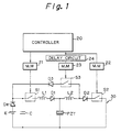
- Fig. 1 shows a device 30 for driving a piezoelectric element PZT controlled by a controller 20, and as shown in Fig. 1, a high potential side of a high voltage generator E is connected to a high potential side of a power condenser C through a diode De, whereby the power condenser C is charged by the high voltage generator E through the diode De.
- the high potential side of the power condenser C is connected to a terminal of the piezoelectric element PZT through a switching means S1, a charging coil L1 and a diode D1, and the node of the diode D1 and the terminal of the piezoelectric element PZT are connected to the ground through a discharging coil L2, a diode D2, and a switching means S2.
- the node of the discharging coil L2 and the diode D2 are connected to the node of the diode De and the power condenser C through a switching means S3 and a diode D3.
- the electrostatic capacity of the power condenser C is extremely larger than that of the piezoelectric element PZT.
- the high voltage generator E generates a voltage as high as 320 (V), and accordingly, the voltage at the high potential side of the power condenser C is approximately 320 (V).
- the device 30 for driving the piezoelectric element is the same as that shown in Fig. 10. Therefore, in Fig. 1, the discharging coil L2, the diode D2 and the switching means S2 constitute a first discharging circuit, and the discharging coil L2, the switching means S3 and the diode D3 constitute a second discharging circuit.
- the controller 20 includes three monostable multivibrators 21, 22 and 23 and a delay circuit 24 connected to the input terminal of the multivibrator 23, and the respective switching means S1, S2 and S3 are controlled by signals output by the corresponding monostable multivibrators 21, 22 and 23.
- the controller 20 outputs an injection start pulse and an injection completion pulse; the monostable multivibrator 21 being actuated by the injection completion pulse, and the monostable multivibrator 22 and the delay circuit 24 being actuated by the injection start pulse.
- the multivibrator 23 is actuated by the signal output from the delay circuit 24 after a fixed time determined by the delay circuit 24 has elapsed after the controller 20 outputs the injection start pulse.
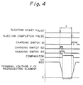
- the controller 20 when the controller 20 outputs the injection start pulse, the output voltage of the monostable multivibrator 22 reaches a high level, and then the output voltage of the monostable multivibrator 23 reaches a high level after a delay. As a result, the switching means S2 is turned ON, and then the switching means S3 is turned ON after a delay. The output voltage of the monostable multivibrator 22 reaches a low level after a predetermined time t2 has passed, and therefore, the switching means S2 is turned ON only for a time t2.
- the switching means S2 When the switching means S2 is turned ON, the voltage at the node of the discharging coil L2 and the diode D2 is abruptly lowered, and thus the discharge of the electric charge in the piezoelectric element PZT is started. Then, the switching means S3 is turned ON. At this time, however, a discharge current does not flow through the switching means S3, but only through the switching means S2. Namely, the electric charge in the piezoelectric element PZT is discharged to the ground through the first discharging circuit comprising the discharging coil L2, the diode D2 and the switching means S2, and as a result, the terminal voltage in of the piezoelectric element PZT gradually falls.
- the switching means S2 when the switching means S2 is turned OFF, energy accumulated in the discharging coil L2 is supplied to the power condenser C through the switching means S3 and the diode D3, i.e., the electric charge in the piezoelectric element PZT is discharged to the high potential side of the power condenser C via the second discharging circuit comprising the discharging coil L2, the switching means S3 and the diode D3, and consequently, a part of the discharge current is recovered by the power condenser C.
- the terminal voltage V of the piezoelectric element PZT is maintained at a constant voltage, and thereafter, the switching means S3 is turned OFF. Namely, the time t3 is determined such that the switching means S3 is turned OFF after the discharging operation is completed.
- the injection completion pulse When an injection time T has passed after the injection start pulse is output, the injection completion pulse is output, and when the injection completion pulse is output, the output voltage of the monostable multivibrator 21 reaches a high level for a predetermined time t1 , and as a result, the switching means S1 is turned ON only for the time t1.
- the switching means S1 When the switching means S1 is turned ON, the electric charge in the power condenser C is charged to the piezoelectric element PZT through the switching means S1, the charging coil L1 and the diode D1.
- the embodiment shown in Fig. 1 illustrates an example wherein the terminal voltage of the piezoelectric element PZT becomes approximately - 60 (V) after the discharging operation is completed, but as mentioned before with reference to Figs. 11D, 11E and 11F, the terminal voltage V of the piezoelectric element PZT after the completion of the discharging operation can be freely changed by changing the ON time t2 of the switching means S2, within a range of from -200 (V) to +200 (V). Namely, in the embodiment shown in Fig. 1, the terminal voltage V of the piezoelectric element PZT after the completion of the discharging operation can be changed over a wide range of negative voltage or positive voltage in accordance with the change of the time t2 determined by the monostable multivibrator 22.
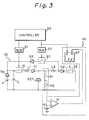
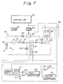
- Fig. 3 shows a second embodiment, wherein a control circuit 40 surrounded by chain lines is added to the device 30 for driving the piezoelectric element PZT shown in Fig. 1.
- This control circuit 40 comprises a pair of series resistances R1 and R2 , a comparator 41 and a bistable multivibrator 42.
- the switching means S2 is controlled by the output signal of the bistable multivibrator 42, and the node of the resistances R1 and R2 is connected to a reversing input terminal of the comparator 41.
- a non-reversing input terminal of the comparator 41 is connected to a reference power source 43, and an output terminal of the comparator 41 is connected to a reset input terminal R of the bistable multivibrator 42.
- the injection start pulse is input to a set input terminal S of the bistable multivibrator 42.
- the output voltage of the bistable multivibrator 42 reaches a high level and the switching means S2 is turned ON, and at the same time, the output voltage of the monostable multivibrator 23 reaches a high level and the switching means S3 is turned ON. Then, the output voltage V of the piezoelectric element PZT falls, and thus the voltage at the node of the resistances R1 and R2 falls and becomes lower than the reference voltage of the reference power source 43, and therefore, the output voltage of the comparator 41 reaches a high level. When the output voltage of the comparator 41 reaches the high level. it becomes a trigger.
- the output voltage of the bistable multivibrator 42 reaches a low level and the switching means S2 is turned OFF.
- the ON time t2 of the switching means S2 is determined by the reference voltage of the reference power source 43.
- the output voltage V of the piezoelectric element PZT after the completion of the discharging operation can be arbitrarily changed within a range of from -200 (V) to +200 (V), by changing the reference voltage of the reference power source 43.
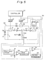
- a third embodiment of the present invention is shown in Fig. 5.
- a control circuit 50 surrounded by chain lines is added to the device 30 for driving the piezoelectric element shown in Fig. 1.
- the control circuit 50 comprises a pair of series resistances R1 and R2 connected in parallel with the piezoelectric element PZT, a minimum peak hold circuit 51, a first comparator 52, a first integrator 53, a second comparator 54, a second integrator 55 and a bistable multivibrator 56.
- the switching means is controlled by the output signal of the bistable multivibrator 56, the node of the resistances R1 and R2 is connected to an input terminal of the minimum peak hold circuit 51, an output terminal of the minimum peak hold circuit 51 is connected to a non-reversing input terminal of the first comparator 52, a reversing input terminal of the first comparator 52 is connected to a reference power source 57, an output terminal of the first comparator 52 is connected to a reversing input terminal of the second comparator 54 through the first integrator 53, an output terminal of the monostable multivibrator 23 is connected to a non-reversing input terminal of the second comparator 54 through the second integrator 55, and an output terminal of the second comparator 54 is connected to a reset input terminal R of the bistable multivibrator 56 and the minimum peak hold circuit 51.
- the injection start pulse is input to a set input terminal S of the bistable multivibrator 56.
- the output voltage of the bistable multivibrator 56 reaches a high level and the switching means S2 is turned ON, and at the same time, the output voltage of the monostable multivibrator 23 reaches a high level and the switching means S3 is turned ON.
- the output voltage V2 of the second integrator 55 begins to increase, and when the output voltage V of the piezoelectric element PZT falls and the output voltage V2 of the second integrator 55 becomes higher than the output voltage V1 of the first integrator 53, the output voltage of the second comparator 54 reaches a high level.
- the output voltage of the comparator 54 reaches the high level, which is a trigger, the output voltage of the bistable multivibrator 42 reaches a low level and the switching means S2 is turned OFF, and simultaneously, the minimum peak hold circuit 51 is reset.
- the minimum terminal voltage V of the piezoelectric element PZT is held by the minimum peak hold circuit 51, and the minimum peak hold circuit 51 outputs the minimum terminal voltage V of the piezoelectric element PZT.
- the output voltage of the minimum peak hold circuit 51 is higher than the reference voltage V o of the reference power source 57, the output voltage of the first comparator 52 reaches a high level, but when output voltage of the minimum peak hold circuit 51 is lower than the reference voltage V o , the output voltage of the first comparator 52 reaches a low level.
- the output voltage of the first comparator 52 is integrated by the first integrator 53 and the result is applied to the reversing input terminal of the second comparator 54.
- the minimum terminal voltage V of the piezoelectric element PZT is lower than the reference voltage V o , the output voltage of the first comparator 52 reaches a low level, and therefore, the output voltage of the first integrator 53 gradually falls.
- the ON time t2 of the switching means S2 is short, and thus the minimum terminal voltage V of the piezoelectric element PZT is increased.
- the minimum terminal voltage V of the piezoelectric element PZT is higher than the reference voltage V o , the output voltage of the first comparator 52 reaches a high level, and therefore, the output voltage of the first integrator 53 gradually increases.
- the ON time t2 of the switching means S2 becomes longer, and thus the minimum terminal voltage V of the piezoelectric element PZT falls. Accordingly, the minimum terminal voltage V of the piezoelectric element PZT can be made to precisely coincide with the reference voltage V o .
- the minimum terminal voltage V of the piezoelectric element PZT can be made to precisely coincide with a desired voltage located within a range of from -200 (V) to +200 (V), which corresponds to the reference voltage V o , by changing the reference voltage V o within a range of from -200 (V) to +200 (V).
- the minimum peak hold circuit 51 may be reset by using a fall of the output voltage of the monostable multivibrator 23 as a trigger. In this case, the output voltage of the minimum peak hold circuit 51 changes as shown in Fig. 8.
- the terminal voltage of the piezoelectric element after the completion of the discharging operation can be controlled to any negative voltage or positive voltage.
Landscapes
- Engineering & Computer Science (AREA)
- Chemical & Material Sciences (AREA)
- Combustion & Propulsion (AREA)
- Mechanical Engineering (AREA)
- General Engineering & Computer Science (AREA)
- Electrical Control Of Air Or Fuel Supplied To Internal-Combustion Engine (AREA)
- General Electrical Machinery Utilizing Piezoelectricity, Electrostriction Or Magnetostriction (AREA)
- Fuel-Injection Apparatus (AREA)
Claims (20)
- Einrichtung zur Ansteuerung eines piezoelektrischen Elements (PZT) mit:
einem Leistungskondensator (C) mit einer hochspannungsseitigen Anschlußklemme;
einer zwischen das piezoelektrische Element und die hochspannungsseitige Anschlußklemme des Leistungskondensators geschalteten ersten Schalteinrichtung (S1) zum Laden des piezoelektrischen Elements unter Verwendung eines hohen Potentials an der hochspannungsseitigen Anschlußklemme des Leistungskondensators;
einer zwischen das piezoelektrische Element und Masse geschalteten ersten Entladeschaltung (L2, D2, S2) mit einer Entladespule (L2) darin, zum Entladen des piezoelektrischen Elements über die erste Entladeschaltung zu Masse;
einer zwischen das piezoelektrische Element und die hochspannungsseitige Anschlußklemme des Leistungskondensators geschalteten zweiten Entladeschaltung (L2, S3, D3) mit einer Entladespule (L2) darin, zum Entladen des piezoelektrischen Elements über die zweite Entladeschaltung zur hochspannungsseitigen Anschlußklemme des Leistungskondensators; einer Entlade-Steuereinrichtung (20, 21, 22, 23, 24) zum Entladen des piezoelektrischen Elements
dadurch gekennzeichnet, daß das piezoelektrische Element nach dem Entladen des piezoelektrischen Elements über die erste Entladeschaltung zu Masse über die zweite Entladeschaltung zur hochspannungsseitigen Anschlußklemme des Leistungskondensators entladen wird. - Einrichtung nach Anspruch 1, bei der die hochspannungsseitige Anschlußklemme des Leistungskondensators mit einer Konstantspannungsquelle verbunden ist, um den Leistungskondensator zu laden.
- Einrichtung nach Anspruch 1, bei der eine Ladespule (L1) in Reihe zu der ersten Schalteinrichtung geschaltet ist.
- Einrichtung nach Anspruch 3, bei der eine eine Durchlaßrichtung von der Ladespule zu dem piezoelektrischen Element ausbildende Diode (D1) zwischen die Ladespule und das piezoelektrische Element geschaltet ist.
- Einrichtung nach Anspruch 1, bei der die Entladespule der ersten Entladeschaltung und die Entladespule der zweiten Entladeschaltung durch die gleiche Entladespule ausgebildet sind.
- Einrichtung nach Anspruch 1, bei der eine eine Durchlaßrichtung von der Entladespule der ersten Entladeschaltung zu Masse ausbildende Diode (D2) zwischen die Entladespule der ersten Entladeschaltung und Masse geschaltet ist.
- Einrichtung nach Anspruch 1, bei der eine eine Durchlaßrichtung von der Entladespule der zweiten Entladeschaltung zur hochspannungsseitigen Anschlußklemme des Leistungskondensators ausbildende Diode (D3) zwischen die Entladespule der zweiten Entladeschaltung und die hochspannungsseitige Anschlußklemme des Leistungskondensators geschaltet ist.
- Einrichtung nach Anspruch 1, bei der die Entlade-Steuereinrichtung mit einer in der ersten Entladeschaltung vorgesehenen zweiten Schalteinrichtung (S2) und einer in der zweiten Entladeschaltung vorgesehenen dritten Schalteinrichtung (S3) versehen ist, wobei die zweite Schalteinrichtung eingeschaltet ist, wenn das piezoelektrische Element entladen wird, die dritte Schalteinrichtung eingeschaltet wird, bevor die zweite Schalteinrichtung ausgeschaltet wird, und die dritte Schalteinrichtung ausgeschaltet wird, nachdem die zweite Schalteinrichtung ausgeschaltet ist.
- Einrichtung nach Anspruch 8, bei der die zweite Schalteinrichtung und die dritte Schalteinrichtung gleichzeitig eingeschaltet werden, wenn das piezoelektrische Element entladen wird.
- Einrichtung nach Anspruch 8, bei der die dritte Schalteinrichtung eingeschaltet wird, wenn eine feste Verzögerungszeit nach dem Einschalten der zweiten Schalteinrichtung vergangen ist.
- Einrichtung nach Anspruch 8, bei der die zweite Schalteinrichtung während des Entladevorgangs des piezoelektrischen Elements ausgeschaltet wird und die dritte Schalteinrichtung ausgeschaltet wird, nachdem der Entladevorgang des piezoelektrischen Elements beendet ist.
- Einrichtung nach Anspruch 11, bei der die Entlade-Steuereinrichtung mit einem monostabilen Multivibrator (22) zum Ansteuern der zweiten Schalteinrichtung und einem monostabilen Multivibrator (23) zum Ansteuern der dritten Schalteinrichtung versehen ist, die zweite Schalteinrichtung nur für eine durch den entsprechenden monostabilen Multivibrator bestimmte Zeit eingeschaltet wird, und die dritte Schalteinrichtung nur für eine durch den entsprechenden monostabilen Multivibrator bestimmte Zeit eingeschaltet wird.
- Einrichtung nach Anspruch 11, bei der die Entlade-Steuereinrichtung mit einer Ansteuer-Steuereinrichtung zum Ansteuern der zweiten Schalteinrichtung im Ansprechen auf die Klemmenspannung des piezoelektrischen Elements und den monostabilen Multivibrator zum Ansteuern der dritten Schalteinrichtung versehen ist, die zweite Schalteinrichtung eingeschaltet wird, während die Klemmenspannung des piezoelektrischen Elements auf eine vorbestimmte Einstellspannung abfällt und die dritte Schalteinrichtung nur für eine durch den monostabilen Multivibrator bestimmte Zeit eingeschaltet wird.
- Einrichtung nach Anspruch 13, bei der die Ansteuer-Steuereinrichtung mit einem Paar von zwischen die Anschlußklemmen des piezolelektrischen Elements geschalteten Widerständen (R1, R2) versehen ist und die zweite Schalteinrichtung eingeschaltet ist, während eine Spannung an dem Knoten des Paars von Widerständen auf eine vorbestimmte Spannung abfällt.
- Einrichtung nach Anspruch 13, bei der die Ansteuer-Steuereinrichtung mit einem Vergleicher (41) zum Vergleichen der Klemmenspannung des piezoelektrischen Elements mit der eingestellten Spannung und einem bistabilen Multivibrator (42) zum Einschalten der zweiten Schalteinrichtung auf der Grundlage des Ausgangs des Vergleichers, während die Klemmenspannung des piezoelektrischen Elements auf die eingestellte Spannung abfällt, versehen ist.
- Einrichtung nach Anspruch 11, bei der die Entlade-Steuereinrichtung mit einer Erfassungseinrichtung (50) zum Erfassen der Klemmenspannung des piezoelektrischen Elements nach dem Beenden des Entladevorgangs, einer Ansteuer-Steuereinrichtung zum Ansteuern der zweiten Schalteinrichtung derart, daß die Klemmenspannung des piezoelektrischen Elements nach dem Entladen eine vorbestimmte eingestellte Spannung wird, und einem monostabilen Multivibrator zum Ansteuern der dritten Schalteinrichtung versehen ist, wobei die dritte Schalteinrichtung nur für eine durch den monostabilen Multivibrator bestimmte Zeit eingeschaltet wird.
- Einrichtung nach Anspruch 16, bei der die Erfassungseinrichtung eine Minimalspitzenwert-Halteschaltung (51) zum Halten der minimalen Klemmenspannung des piezoelektrischen Elements nach dem Entladevorgang umfaßt.
- Einrichtung nach Anspruch 16, bei der die Erfassungseinrichtung eine Minimalspitzenwert-Halteschaltung zum Halten der Klemmenspannung des piezoelektrischen Elements nach dem Entladen des piezoelektrischen Elements, bevor das Laden des piezoelektrischen Elements beginnt, enthält.
- Einrichtung nach Anspruch 16, bei der die Ansteuer-Steuereinrichtung mit einem bistabilen Multivibrator zum Steuern der Einschaltzeit der zweiten Schalteinrichtung versehen ist, wobei die Einschaltzeit verkürzt wird, wenn die Klemmenspannung des piezoelektrischen Elements nach dem Beenden des Entladevorgangs geringer als die eingestellte Spannung wird, und die Einschaltzeit verlängert wird, wenn die Klemmenspannung des piezoelektrischen Elements nach dem Beenden des Entladevorgangs höher als die eingestellte Spannung wird.
- Einrichtung nach Anspruch 19, bei der die Ansteuer-Steuereinrichtung mit einem ersten Vergleicher, einem mit einem Ausgangsanschluß des ersten Vergleichers verbundenen ersten Integrierer, einem zweiten Vergleicher und einem mit einem Ausgangsanschluß des monostabilen Multivibrators verbundenen zweiten Integrierer versehen ist, ein nicht-invertierender Eingangsanschluß des ersten Vergleichers mit einem Ausgangsanschluß der Erfassungseinrichtung verbunden ist, ein invertierender Eingangsanschluß des ersten Vergleichers mit einer Bezugsspannungsquelle verbunden ist, ein nicht-invertierender Eingangsanschluß des zweiten Vergleichers mit einem Ausgangsanschluß des ersten Integrierers verbunden ist, ein invertierender Eingangsanschluß des zweiten Vergleichers mit einem Ausgangsanschluß des zweiten Integrierers verbunden ist, und der bistabile Multivibrator auf der Grundlage des Ausgangssignals des zweiten Vergleichers gesteuert wird.
Applications Claiming Priority (2)
| Application Number | Priority Date | Filing Date | Title |
|---|---|---|---|
| JP148518/90 | 1990-06-08 | ||
| JP2148518A JP2969805B2 (ja) | 1990-06-08 | 1990-06-08 | 圧電素子の駆動装置 |
Publications (3)
| Publication Number | Publication Date |
|---|---|
| EP0460660A2 EP0460660A2 (de) | 1991-12-11 |
| EP0460660A3 EP0460660A3 (en) | 1992-04-01 |
| EP0460660B1 true EP0460660B1 (de) | 1995-03-22 |
Family
ID=15454569
Family Applications (1)
| Application Number | Title | Priority Date | Filing Date |
|---|---|---|---|
| EP91109273A Expired - Lifetime EP0460660B1 (de) | 1990-06-08 | 1991-06-06 | Einrichtung zur Ansteuerung eines piezoelektrischen Elements |
Country Status (4)
| Country | Link |
|---|---|
| US (1) | US5208505A (de) |
| EP (1) | EP0460660B1 (de) |
| JP (1) | JP2969805B2 (de) |
| DE (1) | DE69108297T2 (de) |
Families Citing this family (33)
| Publication number | Priority date | Publication date | Assignee | Title |
|---|---|---|---|---|
| FR2687258A1 (fr) * | 1992-02-06 | 1993-08-13 | Asulab Sa | Dispositif comportant un transducteur piezo-electrique. |
| US5245242A (en) * | 1992-04-13 | 1993-09-14 | Rockwell International Corporation | Efficiency driver system for piezoelectrics |
| JPH0662585A (ja) * | 1992-08-04 | 1994-03-04 | Fujitsu Ltd | 圧電素子駆動回路 |
| DE4237509A1 (de) * | 1992-11-06 | 1994-05-19 | Danfoss As | Verfahren und Schaltungsanordnung zum Aufladen und Entladen einer Last mit einem kapazitiven Anteil |
| JP3085337B2 (ja) * | 1993-01-19 | 2000-09-04 | アイシン精機株式会社 | 内燃機関の燃料噴射制御装置 |
| US5361014A (en) * | 1993-11-10 | 1994-11-01 | Caterpillar Inc. | Apparatus for driving a piezoelectric actuator |
| US6111335A (en) * | 1993-12-28 | 2000-08-29 | Beniamin Acatrinei | Piezoelectric interface analyzer |
| AU1281697A (en) * | 1995-12-04 | 1997-07-14 | Robert Bosch Corporation | Resonant coupled transducer drive |
| DE19632871C2 (de) * | 1996-08-14 | 1998-07-02 | Siemens Ag | Vorrichtung und Verfahren zum Ansteuern wenigstens eines kapazitiven Stellgliedes |
| DE19632872C2 (de) * | 1996-08-14 | 1998-08-13 | Siemens Ag | Vorrichtung und Verfahren zum Ansteuern eines kapazitiven Stellgliedes |
| USRE38470E1 (en) * | 1996-12-18 | 2004-03-23 | Siemens Aktiengesellschaft | Method and device for driving at least one capacitive actuator |
| DE19652809C1 (de) * | 1996-12-18 | 1998-06-10 | Siemens Ag | Verfahren und Vorrichtung zum Ansteuern wenigstens eines kapazitiven Stellgliedes |
| US5856728A (en) * | 1997-02-28 | 1999-01-05 | Motorola Inc. | Power transformer circuit with resonator |
| US5895998A (en) * | 1997-09-18 | 1999-04-20 | Raytheon Company | Piezoelectric drive circuit |
| DE19744236A1 (de) * | 1997-10-07 | 1999-04-08 | Fev Motorentech Gmbh & Co Kg | Verfahren zur verlustarmen periodischen Ansteuerung einer kapazitiven Last, insbesondere eines piezoelektrischen Aktuators |
| US6016052A (en) * | 1998-04-03 | 2000-01-18 | Cts Corporation | Pulse frequency modulation drive circuit for piezoelectric transformer |
| DE19825210C2 (de) * | 1998-04-23 | 2003-09-25 | Gsg Elektronik Gmbh | Schaltungsanordnung zur dynamischen Ansteuerung von keramischen Festkörperaktoren |
| US5969462A (en) * | 1998-06-18 | 1999-10-19 | Cts Corporation | Extensional mode piezoelectric crystal resonator with split electrodes and transformer driving circuit |
| DE19843621B4 (de) * | 1998-09-23 | 2006-03-30 | Siemens Ag | Entladeschaltung für ein kapazitives Stellglied |
| DE19845037C2 (de) * | 1998-09-30 | 2000-11-30 | Siemens Ag | Verfahren und Anordnung zum Ansteuern eines kapazitiven Aktors |
| JP3804312B2 (ja) * | 1998-12-17 | 2006-08-02 | コニカミノルタホールディングス株式会社 | 圧電アクチュエータ及び圧電アクチュエータ駆動装置 |
| DE19903555C2 (de) * | 1999-01-29 | 2001-05-31 | Daimler Chrysler Ag | Vorrichtung zur Steuerung eines Piezoelement-Einspritzventils |
| WO2001033063A1 (en) * | 1999-11-01 | 2001-05-10 | Siemens Automotive Corporation | Control of driver current via low side gates |
| ATE446590T1 (de) * | 2000-04-01 | 2009-11-15 | Bosch Gmbh Robert | Verfahren und vorrichtung zur regelung von spannungen und spannungsgradienten zum antrieb eines piezoelektrischen elements |
| DE60019260T2 (de) * | 2000-04-01 | 2006-02-09 | Robert Bosch Gmbh | Verfahren und Vorrichtung zur zeitgesteuerter Spannungsmessung über einer Vorrichtung in einem Ladungskreis eines piezoelektrischen Element |
| DE60011038T2 (de) * | 2000-04-01 | 2005-07-21 | Robert Bosch Gmbh | Zeit und Fall-kontrolliertes Aktivierungssystem für die Aufladung und die Entladung von piezoelektrischen Elementen |
| JP2002094364A (ja) * | 2000-09-19 | 2002-03-29 | Toshiba Tec Corp | 容量性素子の駆動方法及び駆動装置 |
| FR2829313B1 (fr) * | 2001-09-04 | 2007-03-09 | Renault | Dispositif de commande d'un actuateur piezo-electrique et son procede de mise en oeuvre |
| US6894460B2 (en) * | 2003-01-09 | 2005-05-17 | The Boeing Company | High efficiency passive piezo energy harvesting apparatus |
| US7355320B2 (en) * | 2004-11-10 | 2008-04-08 | Advanced Energy Industries, Inc. | Reactive load resonant drive circuit |
| US7510150B2 (en) * | 2005-09-28 | 2009-03-31 | The Boeing Company | Energy recovery apparatus and method |
| JP4434248B2 (ja) * | 2007-08-22 | 2010-03-17 | 株式会社デンソー | ピエゾアクチュエータ駆動装置 |
| IL187544A0 (en) * | 2007-11-21 | 2008-03-20 | Audiodent Israel Ltd | Circuitry of a low-power piezoelectric driver and method thereof |
Family Cites Families (11)
| Publication number | Priority date | Publication date | Assignee | Title |
|---|---|---|---|---|
| DE3048632A1 (de) * | 1980-12-23 | 1982-07-22 | Siemens AG, 1000 Berlin und 8000 München | Schaltungsanordnung fuer piezoelektrisches stellglied und dergleichen |
| US4732129A (en) * | 1985-04-15 | 1988-03-22 | Nippon Soken, Inc. | Control apparatus for electroexpansive actuator enabling variation of stroke |
| US4688536A (en) * | 1985-06-28 | 1987-08-25 | Toyota Jidosha Kabushiki Kaisha | Drive circuit for an electrostrictive actuator in a fuel injection valve |
| NL8503117A (nl) * | 1985-11-13 | 1987-06-01 | Philips Nv | Hogedrukontladingslamp. |
| JPH0821368B2 (ja) * | 1985-11-18 | 1996-03-04 | 松下電子工業株式会社 | メタルハライドランプ |
| JPS6372381A (ja) * | 1986-09-17 | 1988-04-02 | 株式会社日本自動車部品総合研究所 | 容量性負荷の駆動方法 |
| GB2198604B (en) * | 1986-11-15 | 1991-02-13 | Brother Ind Ltd | Piezoelectric element drive circuit |
| US4966119A (en) * | 1988-01-12 | 1990-10-30 | Toyota Jidosha Kabushiki Kaisha | Fuel injection control device for use in an engine |
| JP2754610B2 (ja) * | 1988-11-09 | 1998-05-20 | 株式会社デンソー | 圧電アクチュエータ駆動装置 |
| EP0371469B1 (de) * | 1988-11-30 | 1995-02-08 | Toyota Jidosha Kabushiki Kaisha | Apparat zum Antreiben eines piezoelektrischen Elements zum Öffnen oder zum Schliessen eines Ventilteils |
| JP2536114B2 (ja) * | 1989-01-18 | 1996-09-18 | トヨタ自動車株式会社 | 圧電素子の駆動装置 |
-
1990
- 1990-06-08 JP JP2148518A patent/JP2969805B2/ja not_active Expired - Fee Related
-
1991
- 1991-06-05 US US07/711,173 patent/US5208505A/en not_active Expired - Lifetime
- 1991-06-06 DE DE69108297T patent/DE69108297T2/de not_active Expired - Fee Related
- 1991-06-06 EP EP91109273A patent/EP0460660B1/de not_active Expired - Lifetime
Also Published As
| Publication number | Publication date |
|---|---|
| DE69108297D1 (de) | 1995-04-27 |
| US5208505A (en) | 1993-05-04 |
| JP2969805B2 (ja) | 1999-11-02 |
| EP0460660A2 (de) | 1991-12-11 |
| DE69108297T2 (de) | 1995-08-31 |
| JPH0444281A (ja) | 1992-02-14 |
| EP0460660A3 (en) | 1992-04-01 |
Similar Documents
| Publication | Publication Date | Title |
|---|---|---|
| EP0460660B1 (de) | Einrichtung zur Ansteuerung eines piezoelektrischen Elements | |
| EP0464443B1 (de) | Steuervorrichtung für ein piezoelektrisches Element | |
| JP2536114B2 (ja) | 圧電素子の駆動装置 | |
| EP0611880B1 (de) | Kraftstoffeinspritz-Regelvorrichtung für eine Brennkraftmaschine | |
| US5130598A (en) | Apparatus for driving a piezoelectric actuator | |
| US4767959A (en) | Method and apparatus for driving capacitive-type load | |
| US5691620A (en) | Battery charging method | |
| US6137208A (en) | Device and method for driving a capacitive actuator | |
| US20020121958A1 (en) | Method and circuit for driving at least one capacitive actuator | |
| JP4499966B2 (ja) | 二次電池の充電回路 | |
| KR100662145B1 (ko) | 하나 이상의 용량성 제어소자를 구동하는 방법 및 장치 | |
| JPH0618134B2 (ja) | ソレノイド駆動器制御ユニット | |
| US5796223A (en) | Method and apparatus for high-speed driving of electromagnetic load | |
| US4112477A (en) | Circuit for energizing a fuel injector valve coil | |
| EP1814167B1 (de) | Steuervorrichtung zur Steuerung der Entladungsdauer eines Piezo-Injektors | |
| US5907466A (en) | Device and process for activating at least two electromagnetic loads | |
| JPH1018888A (ja) | 燃料噴射弁駆動回路 | |
| GB2247366A (en) | A two state constant current battery charging system | |
| JPH11141381A (ja) | 電磁弁駆動回路 | |
| JPH11141382A (ja) | 電磁弁駆動回路 | |
| US20080231245A1 (en) | Current Source and Control Device | |
| JP2890780B2 (ja) | 電磁弁駆動回路 | |
| JP2832000B2 (ja) | 蓄電池充電装置 | |
| JPS6347895B2 (de) | ||
| JP4824187B2 (ja) | 圧電素子の充電のための装置及び方法 |
Legal Events
| Date | Code | Title | Description |
|---|---|---|---|
| PUAI | Public reference made under article 153(3) epc to a published international application that has entered the european phase |
Free format text: ORIGINAL CODE: 0009012 |
|
| 17P | Request for examination filed |
Effective date: 19910705 |
|
| AK | Designated contracting states |
Kind code of ref document: A2 Designated state(s): DE FR GB |
|
| PUAL | Search report despatched |
Free format text: ORIGINAL CODE: 0009013 |
|
| AK | Designated contracting states |
Kind code of ref document: A3 Designated state(s): DE FR GB |
|
| 17Q | First examination report despatched |
Effective date: 19940708 |
|
| GRAA | (expected) grant |
Free format text: ORIGINAL CODE: 0009210 |
|
| AK | Designated contracting states |
Kind code of ref document: B1 Designated state(s): DE FR GB |
|
| REF | Corresponds to: |
Ref document number: 69108297 Country of ref document: DE Date of ref document: 19950427 |
|
| ET | Fr: translation filed | ||
| PLBE | No opposition filed within time limit |
Free format text: ORIGINAL CODE: 0009261 |
|
| STAA | Information on the status of an ep patent application or granted ep patent |
Free format text: STATUS: NO OPPOSITION FILED WITHIN TIME LIMIT |
|
| 26N | No opposition filed | ||
| REG | Reference to a national code |
Ref country code: GB Ref legal event code: IF02 |
|
| REG | Reference to a national code |
Ref country code: GB Ref legal event code: 746 Effective date: 20021008 |
|
| REG | Reference to a national code |
Ref country code: FR Ref legal event code: D6 |
|
| PGFP | Annual fee paid to national office [announced via postgrant information from national office to epo] |
Ref country code: FR Payment date: 20080617 Year of fee payment: 18 |
|
| PGFP | Annual fee paid to national office [announced via postgrant information from national office to epo] |
Ref country code: GB Payment date: 20090603 Year of fee payment: 19 Ref country code: DE Payment date: 20090604 Year of fee payment: 19 |
|
| GBPC | Gb: european patent ceased through non-payment of renewal fee |
Effective date: 20100606 |
|
| REG | Reference to a national code |
Ref country code: FR Ref legal event code: ST Effective date: 20110228 |
|
| PG25 | Lapsed in a contracting state [announced via postgrant information from national office to epo] |
Ref country code: DE Free format text: LAPSE BECAUSE OF NON-PAYMENT OF DUE FEES Effective date: 20110101 |
|
| PG25 | Lapsed in a contracting state [announced via postgrant information from national office to epo] |
Ref country code: FR Free format text: LAPSE BECAUSE OF NON-PAYMENT OF DUE FEES Effective date: 20100630 |
|
| PG25 | Lapsed in a contracting state [announced via postgrant information from national office to epo] |
Ref country code: GB Free format text: LAPSE BECAUSE OF NON-PAYMENT OF DUE FEES Effective date: 20100606 |