EP0460903A2 - Schaltung für künstliche neurale Funktion - Google Patents
Schaltung für künstliche neurale Funktion Download PDFInfo
- Publication number
- EP0460903A2 EP0460903A2 EP91305016A EP91305016A EP0460903A2 EP 0460903 A2 EP0460903 A2 EP 0460903A2 EP 91305016 A EP91305016 A EP 91305016A EP 91305016 A EP91305016 A EP 91305016A EP 0460903 A2 EP0460903 A2 EP 0460903A2
- Authority
- EP
- European Patent Office
- Prior art keywords
- thin film
- resistance state
- resistance
- organic thin
- artificial neural
- Prior art date
- Legal status (The legal status is an assumption and is not a legal conclusion. Google has not performed a legal analysis and makes no representation as to the accuracy of the status listed.)
- Granted
Links
Images

Classifications
-
- G—PHYSICS
- G11—INFORMATION STORAGE
- G11C—STATIC STORES
- G11C11/00—Digital stores characterised by the use of particular electric or magnetic storage elements; Storage elements therefor
- G11C11/54—Digital stores characterised by the use of particular electric or magnetic storage elements; Storage elements therefor using elements simulating biological cells, e.g. neuron
-
- G—PHYSICS
- G06—COMPUTING OR CALCULATING; COUNTING
- G06N—COMPUTING ARRANGEMENTS BASED ON SPECIFIC COMPUTATIONAL MODELS
- G06N3/00—Computing arrangements based on biological models
- G06N3/02—Neural networks
- G06N3/06—Physical realisation, i.e. hardware implementation of neural networks, neurons or parts of neurons
- G06N3/063—Physical realisation, i.e. hardware implementation of neural networks, neurons or parts of neurons using electronic means
Definitions
- the present invention relates to an artificial neural function circuit which is useful in the electric/electronic industries and more particularly in the information processing industry.
- Hopfield has shown that a function of a neural net realized in the form of an impedance circuit constituted by amplifiers, resistors and capacitors converges to a minimum value, making thus it possible to solve combinatorial problems. Further, it has been demonstrated that the neural net can effectively be applied to associative storages, pattern recognition systems, etc. For these reasons, the neural net attracts attention as a promising information processing unit.
- an object of the present invention to provide an artificial neural circuit which is capable of information processings similar to those of the neural system and which can be implemented in a simplified and compact structure while ensuring capability of highly intelligent functions.
- an artificial neural function circuit which incorporates an organic thin film element exhibiting variable resistance states in response to application of electric input signals.
- the organic thin film element holds the resistance state as attained for a predetermined duration even after removal of the applied electric signal.
- the thin film element has such physical property that the direction in which the resistance state is changed (i.e. resistance is increased or decreased) depends on the polarity of the electric input signal.
- a thin film which can exhibit such physical property there may be mentioned a lead phthalocyanine thin film, although the invention is never restricted to the use thereof.
- the organic thin film element incorporated in the artificial neural function circuit according to the invention can be implemented in a much simplified structure when compared with the hitherto known circuit using the existing semiconductor device and thus exhibit excellent practical applicability. Besides, since the organic thin film element can readily be imparted with a great variety of characteristics, realization of a compact structure (microstructurization of elements) can be accomplished while assuring enhanced intelligent functions.
- the organic thin film element when the organic thin film element is capable of holding or maintaining the attained resistance state at least for a predetermined time even after removal of the electric input signal and/or when the direction of change (increase/decrease) of the resistance state depends on the polarity of the electric input signal, as in the case of the lead phthalocyanine thin film, highly intelligent functions as well as microstructurization can be easily realized.
- an organic thin film element Before entering into detailed description of the preferred or exemplary embodiments of the present invention, electric characteristics of an organic thin film element will be discussed by taking as example an element composed of a lead phthalocyanine thin film deposited under vacuum in a thickness of 1.2 ⁇ m and having a bottom electrode mounted on a rear surface and a top electrode mounted on an upper surface.
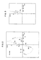
- the top electrode is connected to the ground potential while a plus-minus sweep voltage (electric input signal) is applied to the bottom electrode at a rate of 4 V/sec to thereby cause the resistance of the thin film element to be changed. Then, the thin film element undergoes such a change in resistance as illustrated in Fig. 2.
- the lead phthalocyanine thin film assumes initially a high resistance state R1. However, when the sweep voltage is increased beyond a plus voltage V1, the resistance state of the lead phthalocyanine thin film is changed to a low resistance state R2 after having passed through a negative resistance region. Thereafter, when the sweep voltage exceeds a minus voltage V2, the thin film element resumes the initial high resistance state R1 after passing through a negative resistance region. In this manner, the lead phthalocyanine thin film element reciprocates between the high resistance state R1 and the low resistance state R2 during a single sweep of the applied voltage between values of the opposite polarities.
- the thin film element When the minus voltage sweep is not performed in succession to the low resistance state R2 occurring when the plus voltage V1 is exceeded but the electric input signal is removed, the thin film element is held in the low resistance state R2.
- this low resistance state R2 can not be sustained permanently but the high resistance state R1 is resumed of itself after lapse of a predetermined time period.
- such thin film element may also be made to remain in the low resistance state R2 continuously instead of resuming spontaneously the high resistance state R1 even after lapse of the predetermined time duration.
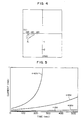
- the rate of change of the resistance value depends on the applied voltage. More specifically, as the voltage applied across the thin film element is higher, the time taken for the element to change from the high resistance state to the low resistance state becomes shorter. Further, the value of resistance in the low resistance state as attained exhibits dependency on the applied voltage. For a given duration of voltage application, the value of the resistance as attained becomes lower, as the applied voltage is increased. It goes without saying that every resistance state as attained is maintained at least for a predetermined time even after removal of the applied voltage. It will thus be appreciated that the lead phthalocyanine thin film element can exhibit a memory function to store the intermediate resistance states between the high resistance state R1 and the low resistance state R2 and thus serve as a multi-value memory element.
- Fig. 6 shows graphically a voltage-current characteristic of a lead phthalocyanine thin film element which slightly differs from that shown in Fig. 2.
- the current rises up steeply in the plus voltage region, and the voltage-current characteristic curve is asymmetrical with reference to the origin 0. Consequently, the lead phthalocyanine thin film element transits to a low resistance state immediately upon application of a voltage in the plus voltage sweep, while restoration to a high resistance state in the minus voltage sweep takes a lot of time.
- transition from the high resistance state to the low resistance state takes place at a high speed, while the transition in the reverse direction is effected only slowly.
- the organic thin film element can readily exhibit highly intelligent functions.
- plasticity of synaptic coupling it is contemplated to mean that the strength or degree of the synaptic coupling varies in dependence on magnitude of input stimulus and a number of times the stimuli are applied.
- plasticity of the synaptic coupling information processing in organisms are made possible.
- the organic thin film element may be made of other material than lead phthalocyanine.
- the electric input signal may be applied in the form of an electric current.
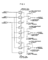
- Fig. 1 shows an artificial neuron function circuit according to an embodiment of the present invention.
- the artificial neural function circuit includes nine organic thin film elements 1 to 9, three operational amplifiers 10 to 12, three input terminals 13 to 15, and three output terminals 19 to 21.
- Reference numerals 22 to 24 denote fixed resistance elements, respectively.
- the organic thin film elements 1 to 3 have one sides connected to associated ones of the input terminals 13 to 15, respectively, and the other sides connected together to an inverted input terminal (minus terminal) of the operational amplifier 10.
- the organic thin film elements 4 to 6 have one sides connected to the input terminals 13 to 15, respectively, and the other sides connected together to an inverted input terminal of the operational amplifier 11.
- the organic thin film elements 7 to 9 have one sides connected to the input terminals 13 to 15 and the other sides connected together to an inverted input terminal of the operational amplifier 12.
- the teacher input terminals 19 to 21 are connected to non-inverted input terminals (plus terminals) of the operational amplifiers 10 to 12, respectively.
- each of the organic thin film elements 1 to 9 is composed of a lead phthalocyanine thin film and can exhibit a variety of characteristics described hereinbefore by reference to Figs. 2 to 5. More specifically, each of the thin film elements is composed of a substrate of an electrically insulating material having a surface formed with a gold film through vapor deposition to serve as a bottom electrode, a lead phthalocyanine thin film (organic thin film) stacked in a thickness of 1.2 ⁇ m through a vacuum vapor deposition method and a gold film formed on the lead phthalocyanine film through vapor deposition to serve as a top electrode.
- each of the organic thin film elements 4 to 9 is applied with a sufficiently high minus voltage to allow these elements to resume the high resistance state.
- the organic thin film elements 1 to 3 which are free of the minus voltage remain in the low resistance state. Consequently, the outputs disappear from the output terminals 17 and 18 with only the output at the terminal 16 being maintained as it is.
- an artificial neural function circuit is implemented in the utterly same structure as that shown in Fig. 1 except that each of the organic thin film elements is imparted with the characteristic illustrated in Fig. 6 in place of that shown in Fig. 2.
- the input voltages of +10 volts, +5 volts and 0 volt are applied to the input terminals 13, 14 and 15, respectively, as in the case of the preceding embodiment.
- applied to the teacher input terminals 19, 20 and 21 are 0 volt, +5 volts and +5 volts, respectively. In this case, only the thin film element 1 assumes the lowest resistance state to thereby allow a highest output signal to be produced from the output terminal 16.
- This state of the artificial neural circuit is maintained even when the voltages applied to the input terminals 13, 14 and 15 and the teacher input terminals 19, 20 and 21 are removed. Accordingly, when the input voltages of the same pattern are subsequently applied to the input terminals 13 to 15, a high output is produced only from the output terminal 16.
- the transition from the low resistance state to the high resistance state takes place at a low speed or rate while transition from the high resistance state to the low resistance state takes place at a high speed, as a result of which learning can be accomplished within a short time with enhanced insusceptibility to lapse of memory. Since the outputs can be obtained from the output terminals 17 and 18, respectively, by changing the input voltage pattern, differences among the input patterns can be discriminatively identified on the basis of the detected outputs.
- Fig. 7 is a chart showing the outputs produced from the output terminals 16 and 17 when two voltage patterns (+10 volts, 0 volt) and (0 volt, +10 volts) are inputted through the input terminals 13 and 14 for teaching an artificial neural circuit according to an embodiment of the invention.
- hollow circles indicate the outputs from the output terminal 16, while solid circles indicate the outputs from the output terminal 17.
- output patterns of (-5 volts, -2 volts) and (-2 volts, -5 volts) can be obtained for the abovementioned input patterns, respectively, which can thus be identified discriminatively from each other.
- a perceptron circuit which is one of the neural networks can be realized in the form of hardware by making use of physical properties of an organic material.
- the input pattern may be of any origin.
- the input pattern may be constituted by output signals of a plurality or variety of sensors.
- the artificial neural function circuit can find application in various types of recognition systems or the like.
- the number of the input signals is assumed to be three. It should however be understood that the number of the input signals may be increased to four or more to thereby impart the artificial neural circuit with more intelligent performance.
- the artificial neural function circuits according to the present invention can be realized in a much simplified and compact structure with remarkably enhanced performance owing to incorporation of the organic thin film element to great advantages in practical applications.
- the organic thin film element can hold the changed resistance state at least for a predetermined time even after removal of the electric input signals.
- the direction in which the resistance state is changed i.e. direction in which the resistance is increased or decreased
- the rate of change,of resistance in the decreasing direction is higher than that in the increasing direction.
Landscapes
- Engineering & Computer Science (AREA)
- Physics & Mathematics (AREA)
- Health & Medical Sciences (AREA)
- Life Sciences & Earth Sciences (AREA)
- Biomedical Technology (AREA)
- Biophysics (AREA)
- Neurology (AREA)
- Theoretical Computer Science (AREA)
- Molecular Biology (AREA)
- General Health & Medical Sciences (AREA)
- Evolutionary Computation (AREA)
- Data Mining & Analysis (AREA)
- Computational Linguistics (AREA)
- Computing Systems (AREA)
- General Engineering & Computer Science (AREA)
- General Physics & Mathematics (AREA)
- Mathematical Physics (AREA)
- Software Systems (AREA)
- Artificial Intelligence (AREA)
- Computer Hardware Design (AREA)
- Thermistors And Varistors (AREA)
Applications Claiming Priority (2)
| Application Number | Priority Date | Filing Date | Title |
|---|---|---|---|
| JP145661/90 | 1990-06-04 | ||
| JP2145661A JPH03255668A (ja) | 1989-10-23 | 1990-06-04 | 擬似神経機能回路 |
Publications (3)
| Publication Number | Publication Date |
|---|---|
| EP0460903A2 true EP0460903A2 (de) | 1991-12-11 |
| EP0460903A3 EP0460903A3 (en) | 1994-08-17 |
| EP0460903B1 EP0460903B1 (de) | 1997-09-10 |
Family
ID=15390171
Family Applications (1)
| Application Number | Title | Priority Date | Filing Date |
|---|---|---|---|
| EP91305016A Expired - Lifetime EP0460903B1 (de) | 1990-06-04 | 1991-06-03 | Schaltung für künstliche neurale Funktion |
Country Status (3)
| Country | Link |
|---|---|
| US (1) | US5223750A (de) |
| EP (1) | EP0460903B1 (de) |
| DE (1) | DE69127585T2 (de) |
Families Citing this family (7)
| Publication number | Priority date | Publication date | Assignee | Title |
|---|---|---|---|---|
| EP0821826B1 (de) * | 1996-02-16 | 2003-07-23 | Koninklijke Philips Electronics N.V. | Einmal beschreibbares, mehrmals lesbares elektrisches speicherelement aus konjugiertem polymer oder oligomer |
| US20070233761A1 (en) * | 2006-04-03 | 2007-10-04 | Mouttet Blaise L | Crossbar arithmetic processor |
| US7576565B2 (en) * | 2006-04-03 | 2009-08-18 | Blaise Laurent Mouttet | Crossbar waveform driver circuit |
| US7302513B2 (en) * | 2006-04-03 | 2007-11-27 | Blaise Laurent Mouttet | Programmable crossbar signal processor |
| US9965251B2 (en) * | 2006-04-03 | 2018-05-08 | Blaise Laurent Mouttet | Crossbar arithmetic and summation processor |
| US8183554B2 (en) * | 2006-04-03 | 2012-05-22 | Blaise Laurent Mouttet | Symmetrical programmable memresistor crossbar structure |
| JP5104052B2 (ja) * | 2007-06-14 | 2012-12-19 | ソニー株式会社 | 抵抗素子、ニューロン素子、及びニューラルネットワーク情報処理装置 |
Family Cites Families (9)
| Publication number | Priority date | Publication date | Assignee | Title |
|---|---|---|---|---|
| GB8431924D0 (en) * | 1984-12-18 | 1985-01-30 | Ici Plc | Optical recording medium |
| US4660166A (en) * | 1985-01-22 | 1987-04-21 | Bell Telephone Laboratories, Incorporated | Electronic network for collective decision based on large number of connections between signals |
| JPS63244678A (ja) * | 1987-03-30 | 1988-10-12 | Mitsubishi Electric Corp | 有機半導体デバイス |
| US4782460A (en) * | 1987-04-06 | 1988-11-01 | American Telephone And Telegraph Company, At&T Bell Laboratories | Computing apparatus comprising a programmable resistor |
| WO1989001228A1 (en) * | 1987-07-28 | 1989-02-09 | Maxdem Incorporated | Electrically settable resistance device |
| FR2621757A1 (fr) * | 1987-10-09 | 1989-04-14 | Thomson Csf | Reseau neuronal programmable a polymere ferroelectrique |
| US4866645A (en) * | 1987-12-23 | 1989-09-12 | North American Philips Corporation | Neural network with dynamic refresh capability |
| US4931763A (en) * | 1988-02-16 | 1990-06-05 | California Institute Of Technology | Memory switches based on metal oxide thin films |
| JPH01300361A (ja) * | 1988-05-28 | 1989-12-04 | Nec Eng Ltd | マイクロプロセッサシステム |
-
1991
- 1991-05-10 US US07/698,148 patent/US5223750A/en not_active Expired - Lifetime
- 1991-06-03 EP EP91305016A patent/EP0460903B1/de not_active Expired - Lifetime
- 1991-06-03 DE DE69127585T patent/DE69127585T2/de not_active Expired - Fee Related
Also Published As
| Publication number | Publication date |
|---|---|
| EP0460903B1 (de) | 1997-09-10 |
| DE69127585T2 (de) | 1998-03-19 |
| US5223750A (en) | 1993-06-29 |
| EP0460903A3 (en) | 1994-08-17 |
| DE69127585D1 (de) | 1997-10-16 |
Similar Documents
| Publication | Publication Date | Title |
|---|---|---|
| US7978510B2 (en) | Stochastic synapse memory element with spike-timing dependent plasticity (STDP) | |
| US4719591A (en) | Optimization network for the decomposition of signals | |
| US5537512A (en) | Neural network elements | |
| EP1349110A2 (de) | Integrierte Halbleiterschaltungsanordnung und Neuro-Element | |
| KR102358622B1 (ko) | 오보닉 임계 스위치를 이용한 인공 뉴런 소자, 그것을 포함하는 인공 신경 칩 및 사용자 장치 | |
| US20120284218A1 (en) | Neuron device and neural network | |
| US20100223220A1 (en) | Electronic synapse | |
| EP0377908A2 (de) | Neurales Netzwerk mit Assoziativspeicher, der durch Beispiele lernt | |
| KR940004486A (ko) | 자기학습형 적화연산회로소자 및 회로 | |
| KR102126791B1 (ko) | 교차점 어레이를 이용한 신경 연결망 및 그 패턴 인식방법 | |
| EP0460903B1 (de) | Schaltung für künstliche neurale Funktion | |
| US20210174173A1 (en) | Circuit Structure and Driving Method Thereof, Neural Network | |
| KR20210023277A (ko) | 단일 게이트의 피드백 전계효과 전자소자를 이용하는 축적 및 발화 뉴런회로 | |
| US5237210A (en) | Neural network accomodating parallel synaptic weight adjustments for correlation learning algorithms | |
| CN113807161A (zh) | 尖峰时序相依可塑性的写入方法及突触数组装置 | |
| CN114970846B (zh) | 一种储备池计算网络的硬件实现方法 | |
| US5444821A (en) | Artificial neuron element with electrically programmable synaptic weight for neural networks | |
| KR970022771A (ko) | 순간 인식 기능을 구비한 연산 회로 및 순간 인식 방법 | |
| Chen et al. | Revisiting memristor properties | |
| Li et al. | Tri-state memristors based on composable discrete devices | |
| JPH03255668A (ja) | 擬似神経機能回路 | |
| Gibertini et al. | Coincidence detection with an analog spiking neuron exploiting ferroelectric polarization | |
| KR102892142B1 (ko) | 이미지 인식 기술에서의 축적 컴퓨팅 시스템 | |
| Moopenn et al. | A neural network for Euclidean distance minimization | |
| Mulaosmanovic et al. | FeFETs for neuromorphic systems |
Legal Events
| Date | Code | Title | Description |
|---|---|---|---|
| PUAI | Public reference made under article 153(3) epc to a published international application that has entered the european phase |
Free format text: ORIGINAL CODE: 0009012 |
|
| AK | Designated contracting states |
Kind code of ref document: A2 Designated state(s): DE FR GB |
|
| PUAL | Search report despatched |
Free format text: ORIGINAL CODE: 0009013 |
|
| AK | Designated contracting states |
Kind code of ref document: A3 Designated state(s): DE FR GB |
|
| 17P | Request for examination filed |
Effective date: 19941117 |
|
| 17Q | First examination report despatched |
Effective date: 19960206 |
|
| GRAG | Despatch of communication of intention to grant |
Free format text: ORIGINAL CODE: EPIDOS AGRA |
|
| GRAH | Despatch of communication of intention to grant a patent |
Free format text: ORIGINAL CODE: EPIDOS IGRA |
|
| GRAH | Despatch of communication of intention to grant a patent |
Free format text: ORIGINAL CODE: EPIDOS IGRA |
|
| GRAA | (expected) grant |
Free format text: ORIGINAL CODE: 0009210 |
|
| AK | Designated contracting states |
Kind code of ref document: B1 Designated state(s): DE FR GB |
|
| REF | Corresponds to: |
Ref document number: 69127585 Country of ref document: DE Date of ref document: 19971016 |
|
| ET | Fr: translation filed | ||
| PLBE | No opposition filed within time limit |
Free format text: ORIGINAL CODE: 0009261 |
|
| STAA | Information on the status of an ep patent application or granted ep patent |
Free format text: STATUS: NO OPPOSITION FILED WITHIN TIME LIMIT |
|
| 26N | No opposition filed | ||
| REG | Reference to a national code |
Ref country code: GB Ref legal event code: 732E |
|
| REG | Reference to a national code |
Ref country code: FR Ref legal event code: TQ |
|
| REG | Reference to a national code |
Ref country code: GB Ref legal event code: 732E |
|
| REG | Reference to a national code |
Ref country code: GB Ref legal event code: IF02 |
|
| REG | Reference to a national code |
Ref country code: FR Ref legal event code: TP |
|
| PGFP | Annual fee paid to national office [announced via postgrant information from national office to epo] |
Ref country code: DE Payment date: 20050526 Year of fee payment: 15 |
|
| PGFP | Annual fee paid to national office [announced via postgrant information from national office to epo] |
Ref country code: GB Payment date: 20050601 Year of fee payment: 15 |
|
| PGFP | Annual fee paid to national office [announced via postgrant information from national office to epo] |
Ref country code: FR Payment date: 20050608 Year of fee payment: 15 |
|
| PG25 | Lapsed in a contracting state [announced via postgrant information from national office to epo] |
Ref country code: GB Free format text: LAPSE BECAUSE OF NON-PAYMENT OF DUE FEES Effective date: 20060603 |
|
| PG25 | Lapsed in a contracting state [announced via postgrant information from national office to epo] |
Ref country code: DE Free format text: LAPSE BECAUSE OF NON-PAYMENT OF DUE FEES Effective date: 20070103 |
|
| GBPC | Gb: european patent ceased through non-payment of renewal fee |
Effective date: 20060603 |
|
| REG | Reference to a national code |
Ref country code: FR Ref legal event code: ST Effective date: 20070228 |
|
| PG25 | Lapsed in a contracting state [announced via postgrant information from national office to epo] |
Ref country code: FR Free format text: LAPSE BECAUSE OF NON-PAYMENT OF DUE FEES Effective date: 20060630 |