EP0461041A2 - Flip-Flop-Schaltung - Google Patents
Flip-Flop-Schaltung Download PDFInfo
- Publication number
- EP0461041A2 EP0461041A2 EP91401486A EP91401486A EP0461041A2 EP 0461041 A2 EP0461041 A2 EP 0461041A2 EP 91401486 A EP91401486 A EP 91401486A EP 91401486 A EP91401486 A EP 91401486A EP 0461041 A2 EP0461041 A2 EP 0461041A2
- Authority
- EP
- European Patent Office
- Prior art keywords
- circuit
- flip
- latch unit
- flop
- terminal
- Prior art date
- Legal status (The legal status is an assumption and is not a legal conclusion. Google has not performed a legal analysis and makes no representation as to the accuracy of the status listed.)
- Granted
Links
Images




Classifications
-
- H—ELECTRICITY
- H03—ELECTRONIC CIRCUITRY
- H03K—PULSE TECHNIQUE
- H03K3/00—Circuits for generating electric pulses; Monostable, bistable or multistable circuits
- H03K3/02—Generators characterised by the type of circuit or by the means used for producing pulses
- H03K3/26—Generators characterised by the type of circuit or by the means used for producing pulses by the use, as active elements, of bipolar transistors with internal or external positive feedback
- H03K3/28—Generators characterised by the type of circuit or by the means used for producing pulses by the use, as active elements, of bipolar transistors with internal or external positive feedback using means other than a transformer for feedback
- H03K3/281—Generators characterised by the type of circuit or by the means used for producing pulses by the use, as active elements, of bipolar transistors with internal or external positive feedback using means other than a transformer for feedback using at least two transistors so coupled that the input of one is derived from the output of another, e.g. multivibrator
- H03K3/286—Generators characterised by the type of circuit or by the means used for producing pulses by the use, as active elements, of bipolar transistors with internal or external positive feedback using means other than a transformer for feedback using at least two transistors so coupled that the input of one is derived from the output of another, e.g. multivibrator bistable
-
- G—PHYSICS
- G01—MEASURING; TESTING
- G01R—MEASURING ELECTRIC VARIABLES; MEASURING MAGNETIC VARIABLES
- G01R31/00—Arrangements for testing electric properties; Arrangements for locating electric faults; Arrangements for electrical testing characterised by what is being tested not provided for elsewhere
- G01R31/28—Testing of electronic circuits, e.g. by signal tracer
- G01R31/317—Testing of digital circuits
- G01R31/3181—Functional testing
- G01R31/3185—Reconfiguring for testing, e.g. LSSD, partitioning
- G01R31/318533—Reconfiguring for testing, e.g. LSSD, partitioning using scanning techniques, e.g. LSSD, Boundary Scan, JTAG
- G01R31/318541—Scan latches or cell details
-
- H—ELECTRICITY
- H03—ELECTRONIC CIRCUITRY
- H03K—PULSE TECHNIQUE
- H03K3/00—Circuits for generating electric pulses; Monostable, bistable or multistable circuits
- H03K3/02—Generators characterised by the type of circuit or by the means used for producing pulses
- H03K3/027—Generators characterised by the type of circuit or by the means used for producing pulses by the use of logic circuits, with internal or external positive feedback
- H03K3/037—Bistable circuits
- H03K3/0372—Bistable circuits of the primary-secondary type
-
- G—PHYSICS
- G06—COMPUTING OR CALCULATING; COUNTING
- G06F—ELECTRIC DIGITAL DATA PROCESSING
- G06F11/00—Error detection; Error correction; Monitoring
- G06F11/22—Detection or location of defective computer hardware by testing during standby operation or during idle time, e.g. start-up testing
- G06F11/2205—Detection or location of defective computer hardware by testing during standby operation or during idle time, e.g. start-up testing using arrangements specific to the hardware being tested
- G06F11/2215—Detection or location of defective computer hardware by testing during standby operation or during idle time, e.g. start-up testing using arrangements specific to the hardware being tested to test error correction or detection circuits
Definitions
- This invention pertains to flip-flops pursuant to the scanning design method used in designing an LSI logic unit.
- a logical operation circuit comprises a sequential circuit and a combinatorial circuit.
- a method of checking failures in a combination circuit is already established.
- D algorithm or PODEM enables such automatic checks.
- a circuit containing a sequential circuit such as a flip-flop, has an undetermined output, even if its input is determined. This is because, to determine its output, it is necessary to prestore such values as initial values in the sequence circuit.
- One of the methods for checking a circuit including such a sequence circuit is the scan designing method.
- the scan designing method flip-flops contained in a logical operation circuit are connected serially, and a scan signal is provided from outside to an input of the flip-flop in the first stage. Since the scan signals sequentially shift the flip-flops and reach the flip-flop in the last stage, a logical operation circuit can check a combination circuit with the shifted value, if the scan signal can be detected to reach the final stage.
- a combination circuit designates a circuit having definite outputs, which do not change unless its input signals change, unique to the combinations of its input signals.
- Figure 1 illustrates the scan designing method and shows the configuration of a logical operation circuit comprising both a sequential circuit and a combinatorial circuit.
- the sequence circuit comprises flip-flops 6, 7 and 8 (FF1, FF2 and FF3).
- a scanning circuit 2 comprises a scan-in terminal 3 and a scan-out terminal 4. The scanning circuit 2 is so connected that the combination circuit 15 is logically separated from flip-flops 6, 7, and 8, while the combination circuit 15 is inspected. That is, flip-flops 6, 7, and 8 do not receive outputs from the combination circuit 15 during its inspection.
- flip-flops 6, 7 and 8 act similarly to shift registers, it becomes possible to treat the output point of flip-flop 6 (FF1) and the input point of flip-flop 8 (FF3) respectively as the signal input pin of the combination circuit 5 and the signal output pin of the combination circuit 5. Conseguently, instead of having to test LSI entirely, it is only necessary to repeat testing every "combination circuit" and judge the existence of a failure.
- Figure 2 shows, in further detail, above described flip-flops 6, 7 and 8, i.e. FF1, FF2 and FF3.
- 9 is a flip-flop
- 10 is a flip-flop in the preceding stage
- 11 is a scan-in signal terminal
- 12 is a terminal for receiving a scanning action control signal
- 13 and 23 are NAND gates
- 14 is a data terminal
- 15 is a terminal for receiving a clock signal
- 16 is a terminal for a clear signal CR
- a terminal 17 of flip-flop 9 is for receiving the clear signal CR
- a terminal 18 of flip-flop 9 is for receiving a preset signal PR
- a terminal 19 of flip-flop 9 transmits the output signal Q.
- 20 and 21 are serially connected flip-flops where the serial connection is logically enabled during a scanning operation.
- 24 is an AND circuit.
- 25 is an OR circuit.
- a scanning operation control signal terminal receives "1", and NAND circuit 13 is enabled, which causes the inversion of the output from flip-flop 10 to be supplied to terminal 18 for receiving the preset signal PR.
- NAND circuit 13 is enabled, which causes the inversion of the output from flip-flop 10 to be supplied to terminal 18 for receiving the preset signal PR.
- Figure 3 is a table of truth value of flip-flops of the type indicated by reference numerals 6, 7, 8 or 9.
- the NAND circuit 22 When the scanning action control signal is high, the NAND circuit 22 is enabled, so then a combination circuit comprising NAND circuit 23, AND circuit 24, NOR circuit 25, etc. may output "0" to the terminal 17 for receiving the clear signal CR, when flip-flop 9 is to be cleared.
- flip-flops 10, 20, 21 and 9 shown in Figure 2 configure logically and serially connected shift registers (F1 through F5 in Figure 4).
- the scanning circuit 2 shown in Figure 1 and described earlier has such a configuration.
- flip-flops 6, 7 and 8 configure the shift register in Figure 1.
- the initial values to be tested are stored in the flip-flops.
- the actions of the combination circuit can be confirmed.
- the scanning circuit does not operate and is connected to the combination circuit shown in Figure 4. That is, the intended actions of an LSI for one clock cycle are performed.
- a failure in an action for a clock signal for scanning is easily detected, since the clock signal is a synchronous signal. Meanwhile, if a failure arises in the circuit of a system asynchronous to the scanning circuit which is connected to an input terminal, such as a circuit supplying the clear signal CR or the preset signal PR, in a scan designing method for judging the actions of a sequence circuit, since scanning actions are being performed, it is difficult to judge whether it is because the clear signal CR or the preset signal PR is unchanging or it is due to a failure.
- An object of the present invention is to provide a flip-flop circuit capable of efficient scan designing by detecting failures in the circuits connected to an input circuit of flip-flops.
- a feature of this invention resides in serially connected flip-flop circuits configuring a scanning circuit for scanning a combination circuit; the scanning circuit connected to the combination circuit; and the flip-flop circuit detects failures of an asynchronous system input circuit connected to the flip-flop circuits.
- the flip-flop circuit configuring a scanning circuit receives a scan-in data at its scan-in terminal and the output of the flip-flop circuit is provided to a combination circuit which operates at a synchronous manner. Then, the output of the combination circuit is again applied to the flip-flop circuit. Then, the output of the flip-flop circuit is scanned out so that the failure of the combination circuit is received.
- An asynchronous system input circuit comprising a combination circuit which operates in an asynchronous manner is connected, for example, a preset or clear terminal of the flip-flop circuit, so that a failure of the asynchronous system input circuit is detected through an scanning-out operation of the flip-flop circuit.
- the serially connected flip-flop circuit is associated with a combination circuit and configuring a scanning circuit for scanning the combination circuit.
- the flip-flop circuit detects failures in an asynchronous system input circuit connected to the flip-flop circuit, when the combination circuit comprise a synchronous system input circuit providing the input to the data terminal of the flip-flop circuit and an asynchronous system input circuit providing the input to the preset or clear terminal of the flip-flop circuit.
- the flip-flops configuring a scanning circuit can be controlled to receive or not to receive data supplied by asynchronous system input signals in synchronization with clock signals. That is, the configuration enables a slave latch unit to be preset or cleared independently of presenting or clearing its master latch unit, where both the slave latch unit and the master latch unit are in the same flip-flop circuit.
- a flip-flop of the slave latch unit receives a preset signal or a clear signal, i.e. an asynchronous system input signal supplied to a flip-flop of the master latch unit, since an expected output signal must be obtained at the output of the flip-flops, if an output signal other than the expected output signal is obtained, a failure in the asynchronous system input circuit is detected.
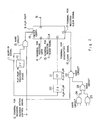
- FIG. 5 illustrates a case in which a common delayed type flip-flop is used.
- 26 is a flip-flop in the scanning circuit; 31 is a master latch unit of flip-flop 26; 32 is a slave latch unit of flip-flop 26; 33-1 and 33-2 are terminals for receiving the preset signal PR respectively for the master latch unit 31 and the slave latch unit 32 in flip-flop 26; 34-1 and 34-2 are terminals for receiving the clear signal CL respectively for the master latch unit 31 and the slave latch unit 32 in flip-flop 26; 35-1 and 35-2 are terminals for receiving test control signals; 36-1 through 36-4 are OR operation circuits, 48 is a data input terminal; 49 is a scan-in input terminal; 50 is a clock signal input terminal; 51 and 52 are input terminals of shift clock signals A and B; 46 is a terminal Q for data output; and 47 is a terminal Q for data output.
- Flip-flop 26 operate ordinarily as a delayed type flip-flop by supplying clock signals to a terminal 39 for clock signal CLK. That is, when clock signal CLK is "1", the master latch unit 31 inputs data D supplied from the data input terminal 37 and fixes the value when clock signal CLK changes from "0" to "1".
- the master latch unit 31 can be preset or cleared, and it is only the master latch unit 31 that can be preset or cleared. Thereafter, "1" is supplied again to enable shifting to the succeeding stage of flip-flop 26.
- the asynchronous system signal comprises a combination circuit which produce an asynchronous system signal to the flip-flops.
- Figure 6 illustrates in further detail the configuration shown in Figure 5.
- transmission gates 37-1 and 37-2 in the master latch unit 31 respond to the clock signal CK.
- transmission gates 38-1 and 38-2 in the master latch unit 31 respond to shift clock signal A.
- Transmission gates 39-1 and 39-2 in the slave latch unit 32 respond to responding to shift clock signal CK.
- Transmission gates 40-1 and 40-2 in the master latch unit 31 respond to clock signals for shift registers B.
- 41-1 and 41-2 are logical operation circuits in the master latch unit 31.
- 42-1 and 42-2 are logical operation circuits in the slave latch unit 32.
- 35-1 through 35-4 are terminals for receiving test control signals.
- transmission gates 37-1, 38-1, 39-1 and 40-1 are off, when transmission gates 37-2, 38-2, 39-2 and 40-2 are on, and that transmission gates 37-1, 38-1, 39-1 and 40-1 are off, when transmission gates 37-2, 38-2, 39-2 and 40-2 are on.
- the transmission gates 37-1 through 40-2 and the logical operation circuits 41-1 through 42-2 together configure the latch units 31 and 32 encircled by dashed lines.
- the clock signals supplied from terminal CK ordinarily cause delayed type flip-flop operations.
- terminals 35-1 and 35-2 for receiving test control input signals SM, terminals 35-3 and 35-4 for receiving test control input signals TM, and terminals 44-1 and 45-1 for receiving shift clock signals A and B are all set to "0".
- clock signal CK is in "0"
- the master latch unit 31 receives data input D, which is transmitted to the slave latch unit 32 when clock signal CK rises, and data Q and XQ are outputted from terminals 46 and 47.
- the transfer gates 37-1 through 40-2 are on when supplied with voltages of reverse polarities to the arrow direction.
- transfer gate 38-2 Since shift clock signal A is ordinarily "0", transfer gate 38-2 is turned on. Therefore, transfer gate 37-2 receives the same binary value as the input. This change causes the already inputted binary value to be received, which is independent of later inputted binary values.
- the binary value outputted from NAND gate 41-1 (the received binary value) is the reversed or the complementary binary value of D and is supplied to the slave latch unit 32.
- clock signal CK is "1"
- both shift clock signal A and shift clock signal B are "0".
- transfer gates 40-1 and 39-1 are on, and transfer gates 40-2 and 39-2 are off.
- NAND gate 42-1 is on, its output is the same as the binary value received by the master latch unit 31( which is the complement of the memorized binary value).
- Output XQ is the complement of the received binary value.
- Output Q is the same as the received binary value.
- the slave latch unit 32 receives the binary value received from the master latch unit 31, in a similar way to the master latch unit 31.
- the master latch unit 31 and the slave latch unit 32 sequentially shift the received binary values.
- shift clock signals A and B are supplied to terminals 44-1 and 44-2 for receiving shift clocks A and B having a phase difference of about one-hundred eighty (180) degrees and a timing difference at least equivalent to one pulse.
- clock signal CK remains at "1"
- test control signals SM and TM are "1”
- transfer gates 37-2 and 39-1 are on and transfer gates 37-1 and 39-2 are off, and NAND gates 41-1, 41-2, 42-1 and 42-2 are on.
- the master latch unit 32 upon receipt of shift clock signal A being "1", the master latch unit 32 receives scan-in signal SI, and the binary value at that time is latched (i.e. received) on receiving "0". Then, the slave latch unit 32 is inputted with this binary value when shift clock signal B is "0", and receives it when shift clock signal B is "1".
- serial-in serial-out mode When a scanning test is performed, there are two operating modes, namely, the serial-in serial-out mode and the parallel-in and parallel-out mode.
- the serial-in serial-out mode is used between times T1 and T2.
- data is transmitted from terminal 49 (the terminal for receiving scan-in signal SI) shown in Figure 6 to the master latch unit 31.
- terminal 49 the terminal for receiving scan-in signal SI
- operation as a shift register is performed properly.
- the parallel-in parallel-out mode is used between times T2 and T3. This mode is created, by supplying "0" to terminals 35-1 and 35-2 for receiving test control signal SM and "1" to terminals 35-3 and 35-4 for receiving test control signal TM.
- a pulse is only once supplied to terminal 43-0 for receiving clock signal CK only the master latch unit 31 latches a clear/preset signal input.
- the operating mode reverts to the serial-in serial-out mode.
- Data received by respective flip-flops is transmitted on receiving clock signals A and B, to terminal 46 for transmitting data outputs XQ and the data is then available for testing the combinatorial circuits.
- the above description can be summarized as follows.
- the period between times T1 and T2 is put in the serial-in serial-out mode, and the values to be tested are stored serially.
- the period between times T2 and T3 is put in the parallel-in parallel-out mode, and by performing an asynchronous system circuit action, such as presetting or clearing, the result is stored in the slave latch unit 32.
- the period after time T3 is put back in the serial-in and serial-out mode and the above result is read again to be confirmed.
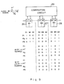
- Figure 8 shows the connection of serially connected three stage flip-flops.
- 26, 27 and 28 are all delayed type flip-flops
- 29 is a combination circuit e.g. similar to the combination circuit 5 shown in Figure 6.
- Terminal SO receives a scan-out signal from the terminal for output Q of flip-flop 28.
- Terminal SO is an output signal terminal for scanning when LSI is checked, i.e.
- a combination circuit 29 is supplied with predetermined signals to input terminals In of the combination circuit 29, so that the signal from the terminal for output Q of each flip-flop is transmitted to the terminal for serial-in SI in the succeeding stage.
- signals are supplied from the terminals for test control signals SM and TM, and clock signal CK and shift clock signals A and B are used, as described earlier, it becomes possible to detect failures in clear/preset signal circuits.
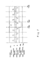
- FIG 9 illustrates how the master latch unit 31 and slave latch unit 32 shown in Figure 8 change their outputs in correspondence with the changes in their inputs.
- Flip-flop 26 is explained first.
- Input D1 is "1" at phase P1, at this time, the master latch unit 31 has not received an input, and is in a preexisting state. (The state is expressed as X, because it is not definite.)
- phase P2 i.e. when clock signal is "0", the master latch unit 31 receives data and its output (M1) becomes "1".
- phase P3 the slave latch unit 32 receives "1", and its output (Q1 ) becomes “1".
- phase P3 after clock signal CK rises, no matter how input D1 changes, its output remains “1". This is similar for flip-flops 27 and 28.
- Figure 9 shows a case where flip-flop 27 receives "0" in phase P1 and output Q is “1”, and a case where flip-flop 29 receives "1" and output Q is "1".
- the master latch unit 31 receives the clearing result. Consequently, by changing the mode to the serial-in serial-out mode thence, the position of the object serial data is cleared and thus has the value "0", which ascertains the normal operation. This is similar to a preset case.
- this invention enables failures in signal supplied from an asynchronous system input terminal to flip-flop circuits used for scanning to be promptly detected.
Landscapes
- Engineering & Computer Science (AREA)
- General Engineering & Computer Science (AREA)
- Physics & Mathematics (AREA)
- General Physics & Mathematics (AREA)
- Power Engineering (AREA)
- Tests Of Electronic Circuits (AREA)
- Test And Diagnosis Of Digital Computers (AREA)
Applications Claiming Priority (2)
| Application Number | Priority Date | Filing Date | Title |
|---|---|---|---|
| JP147751/90 | 1990-06-06 | ||
| JP2147751A JP2567972B2 (ja) | 1990-06-06 | 1990-06-06 | フリップフロップ回路及び半導体集積回路 |
Publications (3)
| Publication Number | Publication Date |
|---|---|
| EP0461041A2 true EP0461041A2 (de) | 1991-12-11 |
| EP0461041A3 EP0461041A3 (en) | 1994-06-22 |
| EP0461041B1 EP0461041B1 (de) | 1997-12-17 |
Family
ID=15437325
Family Applications (1)
| Application Number | Title | Priority Date | Filing Date |
|---|---|---|---|
| EP91401486A Expired - Lifetime EP0461041B1 (de) | 1990-06-06 | 1991-06-06 | Flip-Flop-Schaltung |
Country Status (5)
| Country | Link |
|---|---|
| US (1) | US5440569A (de) |
| EP (1) | EP0461041B1 (de) |
| JP (1) | JP2567972B2 (de) |
| KR (1) | KR950013403B1 (de) |
| DE (1) | DE69128439T2 (de) |
Families Citing this family (11)
| Publication number | Priority date | Publication date | Assignee | Title |
|---|---|---|---|---|
| JP2748069B2 (ja) * | 1992-05-19 | 1998-05-06 | 三菱電機株式会社 | フリップフロップ回路 |
| US5754070A (en) * | 1996-11-19 | 1998-05-19 | Vlsi Technology, Inc. | Metastableproof flip-flop |
| US6260164B1 (en) | 1998-07-31 | 2001-07-10 | International Business Machines Corporation | SRAM that can be clocked on either clock phase |
| JP2003344500A (ja) * | 2002-05-29 | 2003-12-03 | Nec Electronics Corp | マクロテスト回路 |
| CN100554655C (zh) * | 2004-12-14 | 2009-10-28 | 迪普路株式会社 | 柴油发动机的废气净化装置及控制装置 |
| EP1865601A1 (de) * | 2006-06-08 | 2007-12-12 | STMicroelectronics S.r.l. | Asynchrones RS-Flip-Flop mit Testmodus |
| KR102033291B1 (ko) | 2013-06-14 | 2019-10-17 | 삼성전자 주식회사 | 반도체 장치 및 그 구동 방법 |
| KR102193978B1 (ko) | 2019-01-04 | 2020-12-22 | 주식회사 두리파워 | 다목적 신축가능한 수거함 |
| JP7295682B2 (ja) * | 2019-03-29 | 2023-06-21 | ローム株式会社 | フリップフロップ回路及びデータ処理装置 |
| CN114067863B (zh) * | 2020-10-12 | 2025-04-29 | 台积电(南京)有限公司 | 半导体器件及其制造方法 |
| US12597927B2 (en) * | 2023-04-21 | 2026-04-07 | Stmicroelectronics International N.V. | Flip-flop with self correction |
Family Cites Families (10)
| Publication number | Priority date | Publication date | Assignee | Title |
|---|---|---|---|---|
| JPS5779727A (en) * | 1980-11-06 | 1982-05-19 | Seiko Epson Corp | Flip-flop circuit |
| JPS6179318A (ja) * | 1984-09-27 | 1986-04-22 | Fujitsu Ltd | フリツプフロツプ回路 |
| JPS62143513A (ja) * | 1985-12-18 | 1987-06-26 | Hitachi Ltd | マスタスレ−ブ・フリツプフロツプ |
| JPS62226071A (ja) * | 1986-03-28 | 1987-10-05 | Sony Corp | Rsフリツプフロツプ回路 |
| JPH0785099B2 (ja) * | 1986-08-04 | 1995-09-13 | 三菱電機株式会社 | 半導体集積回路装置 |
| KR910002236B1 (ko) * | 1986-08-04 | 1991-04-08 | 미쓰비시 뎅기 가부시끼가이샤 | 반도체집적회로장치 |
| JPH0682146B2 (ja) * | 1986-12-22 | 1994-10-19 | 日本電気株式会社 | スキヤンパス方式の論理集積回路 |
| EP0292116A3 (de) * | 1987-05-05 | 1990-08-01 | Control Data Corporation | Prüfsystem für VLSI-Schaltungen |
| US5047710A (en) * | 1987-10-07 | 1991-09-10 | Xilinx, Inc. | System for scan testing of logic circuit networks |
| JPH0654344B2 (ja) * | 1988-09-07 | 1994-07-20 | 株式会社豊田中央研究所 | スキャンパス回路 |
-
1990
- 1990-06-06 JP JP2147751A patent/JP2567972B2/ja not_active Expired - Fee Related
-
1991
- 1991-06-06 DE DE69128439T patent/DE69128439T2/de not_active Expired - Fee Related
- 1991-06-06 EP EP91401486A patent/EP0461041B1/de not_active Expired - Lifetime
- 1991-06-07 KR KR1019910009421A patent/KR950013403B1/ko not_active Expired - Fee Related
-
1994
- 1994-02-14 US US08/195,606 patent/US5440569A/en not_active Expired - Fee Related
Also Published As
| Publication number | Publication date |
|---|---|
| JPH0440113A (ja) | 1992-02-10 |
| EP0461041B1 (de) | 1997-12-17 |
| KR950013403B1 (ko) | 1995-11-08 |
| DE69128439D1 (de) | 1998-01-29 |
| DE69128439T2 (de) | 1998-04-09 |
| US5440569A (en) | 1995-08-08 |
| KR920001834A (ko) | 1992-01-30 |
| JP2567972B2 (ja) | 1996-12-25 |
| EP0461041A3 (en) | 1994-06-22 |
Similar Documents
| Publication | Publication Date | Title |
|---|---|---|
| US5517108A (en) | Flip-flop circuit in a scanning test apparatus | |
| US5519714A (en) | Testable scan path circuit operable with multi-phase clock | |
| US5130568A (en) | Scannable latch system and method | |
| US6819140B2 (en) | Self-synchronous logic circuit having test function and method of testing self-synchronous logic circuit | |
| KR940003082B1 (ko) | 다기능 스캔 플립플롭 | |
| US4597042A (en) | Device for loading and reading strings of latches in a data processing system | |
| US5459736A (en) | Scan path circuit for testing multi-phase clocks from sequential circuits | |
| JP2725258B2 (ja) | 集積回路装置 | |
| EP0560500B1 (de) | Verfahren und Gerät zum Prüfen von Ein-/Ausgabeverbindungen des Randsteckverbinders einer Schaltkreiskarte mit Boundary Scan | |
| US6873197B2 (en) | Scan flip-flop circuit capable of guaranteeing normal operation | |
| US7398442B2 (en) | Electronic circuit with asynchronously operating components | |
| WO1987000292A1 (en) | On chip test system for configurable gate arrays | |
| EP0319187B1 (de) | Kopplung der Abtastdatenwege | |
| US5450418A (en) | Pseudo master slave capture mechanism for scan elements | |
| EP0289158B1 (de) | Diagnosegerät für ein Datenverarbeitungssystem | |
| US5440569A (en) | Flip-flop circuits for testing LSI gate arrays | |
| US20230259433A1 (en) | Systems and methods to test an asychronous finite machine | |
| US5471152A (en) | Storage element for delay testing | |
| US6073260A (en) | Integrated circuit | |
| US5894213A (en) | Semiconductor integrated circuit having a plurality of flip-flops | |
| EP0590575B1 (de) | Steuerschaltung zum Testen eines Abfragepfades | |
| US6182256B1 (en) | Scan flip-flop that simultaneously holds logic values from a serial load and a subsequent parallel load | |
| US5848075A (en) | Test device employing scan path having circuitry at switches between a scan in signal transmitted and previously held at a predetermined clock timing | |
| EP0151694B1 (de) | Logische Schaltung mit eingebauter Selbsttestfunktion | |
| EP0454052B1 (de) | Datenverarbeitungsvorrichtung mit Prüfschaltung |
Legal Events
| Date | Code | Title | Description |
|---|---|---|---|
| PUAI | Public reference made under article 153(3) epc to a published international application that has entered the european phase |
Free format text: ORIGINAL CODE: 0009012 |
|
| AK | Designated contracting states |
Kind code of ref document: A2 Designated state(s): DE FR GB |
|
| PUAL | Search report despatched |
Free format text: ORIGINAL CODE: 0009013 |
|
| AK | Designated contracting states |
Kind code of ref document: A3 Designated state(s): DE FR GB |
|
| 17P | Request for examination filed |
Effective date: 19941027 |
|
| 17Q | First examination report despatched |
Effective date: 19950929 |
|
| GRAG | Despatch of communication of intention to grant |
Free format text: ORIGINAL CODE: EPIDOS AGRA |
|
| GRAG | Despatch of communication of intention to grant |
Free format text: ORIGINAL CODE: EPIDOS AGRA |
|
| GRAG | Despatch of communication of intention to grant |
Free format text: ORIGINAL CODE: EPIDOS AGRA |
|
| GRAH | Despatch of communication of intention to grant a patent |
Free format text: ORIGINAL CODE: EPIDOS IGRA |
|
| GRAH | Despatch of communication of intention to grant a patent |
Free format text: ORIGINAL CODE: EPIDOS IGRA |
|
| GRAA | (expected) grant |
Free format text: ORIGINAL CODE: 0009210 |
|
| AK | Designated contracting states |
Kind code of ref document: B1 Designated state(s): DE FR GB |
|
| REF | Corresponds to: |
Ref document number: 69128439 Country of ref document: DE Date of ref document: 19980129 |
|
| ET | Fr: translation filed | ||
| PLBE | No opposition filed within time limit |
Free format text: ORIGINAL CODE: 0009261 |
|
| STAA | Information on the status of an ep patent application or granted ep patent |
Free format text: STATUS: NO OPPOSITION FILED WITHIN TIME LIMIT |
|
| 26N | No opposition filed | ||
| REG | Reference to a national code |
Ref country code: GB Ref legal event code: IF02 |
|
| PGFP | Annual fee paid to national office [announced via postgrant information from national office to epo] |
Ref country code: GB Payment date: 20020605 Year of fee payment: 12 |
|
| PGFP | Annual fee paid to national office [announced via postgrant information from national office to epo] |
Ref country code: FR Payment date: 20020610 Year of fee payment: 12 |
|
| PGFP | Annual fee paid to national office [announced via postgrant information from national office to epo] |
Ref country code: DE Payment date: 20020612 Year of fee payment: 12 |
|
| PG25 | Lapsed in a contracting state [announced via postgrant information from national office to epo] |
Ref country code: GB Free format text: LAPSE BECAUSE OF NON-PAYMENT OF DUE FEES Effective date: 20030606 |
|
| PG25 | Lapsed in a contracting state [announced via postgrant information from national office to epo] |
Ref country code: DE Free format text: LAPSE BECAUSE OF NON-PAYMENT OF DUE FEES Effective date: 20040101 |
|
| GBPC | Gb: european patent ceased through non-payment of renewal fee |
Effective date: 20030606 |
|
| PG25 | Lapsed in a contracting state [announced via postgrant information from national office to epo] |
Ref country code: FR Free format text: LAPSE BECAUSE OF NON-PAYMENT OF DUE FEES Effective date: 20040227 |
|
| REG | Reference to a national code |
Ref country code: FR Ref legal event code: ST |