EP0461254A1 - Procede d'illumination en couleur composite et illumination par bandes de longueurs d'onde dans un detecteur a double foyer utilisant l'aberration chromatique - Google Patents
Procede d'illumination en couleur composite et illumination par bandes de longueurs d'onde dans un detecteur a double foyer utilisant l'aberration chromatique Download PDFInfo
- Publication number
- EP0461254A1 EP0461254A1 EP90900999A EP90900999A EP0461254A1 EP 0461254 A1 EP0461254 A1 EP 0461254A1 EP 90900999 A EP90900999 A EP 90900999A EP 90900999 A EP90900999 A EP 90900999A EP 0461254 A1 EP0461254 A1 EP 0461254A1
- Authority
- EP
- European Patent Office
- Prior art keywords
- ray
- wavelength
- rays
- chromatic aberration
- lens system
- Prior art date
- Legal status (The legal status is an assumption and is not a legal conclusion. Google has not performed a legal analysis and makes no representation as to the accuracy of the status listed.)
- Granted
Links
- 230000004075 alteration Effects 0.000 title claims abstract description 36
- 238000000034 method Methods 0.000 title claims description 28
- 238000005286 illumination Methods 0.000 title claims description 24
- 239000002131 composite material Substances 0.000 title 1
- 230000003287 optical effect Effects 0.000 claims description 12
- 239000010408 film Substances 0.000 description 28
- 238000010586 diagram Methods 0.000 description 18
- 239000010410 layer Substances 0.000 description 17
- 238000002310 reflectometry Methods 0.000 description 16
- 230000008569 process Effects 0.000 description 15
- 230000004888 barrier function Effects 0.000 description 9
- 238000001514 detection method Methods 0.000 description 8
- 230000000694 effects Effects 0.000 description 7
- VYPSYNLAJGMNEJ-UHFFFAOYSA-N Silicium dioxide Chemical compound O=[Si]=O VYPSYNLAJGMNEJ-UHFFFAOYSA-N 0.000 description 6
- 239000004065 semiconductor Substances 0.000 description 6
- 239000000463 material Substances 0.000 description 5
- 238000010521 absorption reaction Methods 0.000 description 4
- 230000008859 change Effects 0.000 description 4
- 239000006185 dispersion Substances 0.000 description 4
- 238000002474 experimental method Methods 0.000 description 4
- 230000031700 light absorption Effects 0.000 description 4
- 239000002356 single layer Substances 0.000 description 4
- 239000011248 coating agent Substances 0.000 description 3
- 238000000576 coating method Methods 0.000 description 3
- 229910052681 coesite Inorganic materials 0.000 description 3
- 229910052906 cristobalite Inorganic materials 0.000 description 3
- 238000010438 heat treatment Methods 0.000 description 3
- 230000006872 improvement Effects 0.000 description 3
- 229910021420 polycrystalline silicon Inorganic materials 0.000 description 3
- 239000000377 silicon dioxide Substances 0.000 description 3
- 235000012239 silicon dioxide Nutrition 0.000 description 3
- 229910052682 stishovite Inorganic materials 0.000 description 3
- 229910052905 tridymite Inorganic materials 0.000 description 3
- -1 Science Forum Co.Ltd Substances 0.000 description 2
- 229910052581 Si3N4 Inorganic materials 0.000 description 2
- XAGFODPZIPBFFR-UHFFFAOYSA-N aluminium Chemical compound [Al] XAGFODPZIPBFFR-UHFFFAOYSA-N 0.000 description 2
- 229910052782 aluminium Inorganic materials 0.000 description 2
- 239000006117 anti-reflective coating Substances 0.000 description 2
- 230000015572 biosynthetic process Effects 0.000 description 2
- 238000005520 cutting process Methods 0.000 description 2
- 238000013461 design Methods 0.000 description 2
- 230000006866 deterioration Effects 0.000 description 2
- 238000009826 distribution Methods 0.000 description 2
- 239000011521 glass Substances 0.000 description 2
- 229910052736 halogen Inorganic materials 0.000 description 2
- 150000002367 halogens Chemical class 0.000 description 2
- 238000004886 process control Methods 0.000 description 2
- 230000003595 spectral effect Effects 0.000 description 2
- 239000000758 substrate Substances 0.000 description 2
- 239000010409 thin film Substances 0.000 description 2
- 229910005171 Si3O4 Inorganic materials 0.000 description 1
- 239000006096 absorbing agent Substances 0.000 description 1
- 150000001875 compounds Chemical class 0.000 description 1
- 238000003708 edge detection Methods 0.000 description 1
- 238000011156 evaluation Methods 0.000 description 1
- 230000010354 integration Effects 0.000 description 1
- 238000004519 manufacturing process Methods 0.000 description 1
- 238000012986 modification Methods 0.000 description 1
- 230000004048 modification Effects 0.000 description 1
- 230000009467 reduction Effects 0.000 description 1
- 230000000007 visual effect Effects 0.000 description 1
Images






Classifications
-
- G—PHYSICS
- G03—PHOTOGRAPHY; CINEMATOGRAPHY; ANALOGOUS TECHNIQUES USING WAVES OTHER THAN OPTICAL WAVES; ELECTROGRAPHY; HOLOGRAPHY
- G03F—PHOTOMECHANICAL PRODUCTION OF TEXTURED OR PATTERNED SURFACES, e.g. FOR PRINTING, FOR PROCESSING OF SEMICONDUCTOR DEVICES; MATERIALS THEREFOR; ORIGINALS THEREFOR; APPARATUS SPECIALLY ADAPTED THEREFOR
- G03F9/00—Registration or positioning of originals, masks, frames, photographic sheets or textured or patterned surfaces, e.g. automatically
- G03F9/70—Registration or positioning of originals, masks, frames, photographic sheets or textured or patterned surfaces, e.g. automatically for microlithography
Definitions
- the present invention relates to illumination methods with plural wavelength rays and with wavelength-band rays when a double-focus optical apparatus utilizing chromatic aberration is applied to a position detector such as an X-ray exposure apparatus.
- a stepper such as an X-ray exposure apparatus, it is necessary to adjust a mask and a wafer in place with a high accuracy.
- a resist film, transparent film and the like are provided on a surface of a wafer. Since these films are not uniformly formed, a reflection intensity of an alignment mark on the wafer varies sinusoidally due to a standing wave effect based on optical interferences and a relative intensity of signal rays to detect the alignment mark varies largely, resulting in that an accuracy of alignment is remarkably reduced.
- a stepper manufactured by CENSOR company two rays of wavelengths of 547nm (e ray) and 578nm (d ray) are employed as an alignment ray and when a sufficient signal ray is not obtained by one of the rays, a changeover to the other wavelength ray is made to conduct an alignment operation.
- e ray e ray
- d ray 578nm
- Fig.15 The practical hand-book of apparatus for manufacturing semiconductors, Science Forum Co.Ltd, PP.224 to 225, December 25. 1984).
- LFF Process Control Division reports sinusoidal variation in reflection intensity due to interferences caused by each of two rays of wavelengths of 405nm (h ray) and 436nm (g ray) and variation in reflection intensity due to interferences caused by plural wavelength rays of g ray + h ray and g ray + h ray + i ray (LEE Corporation Process Control Division (60), Trapelo Road Walhm, Massachusetts 02154, (617) 890 to 2000).
- a reflectivity of a single layer film where r 1.0 represents an amplitude reflectivity of a wafer mark to the first layer film and r 2.1 represents an amplitude reflectivity of the first layer film to the atmosphere.
- a reflectivity of a two-layer film Let it be that r 3.2 represents an amplitude reflectivity of the second layer to the atmosphere, n0 represents a refractive index of a wafer, k0 represents an attenuation factor of a wafer, n1 and n2 represent respective refractive indexes of first and second layer film, n3 represents a refractive index of air, ⁇ represetnts a wavelength of incident ray and d1 and d2 represent respective thickness of first and second layer film.
- a reflection intensity of a wafer mark depends upon a refractive index and film thickness of a material formed on a mark and varies sinusoidally with variation of the material.
- Table 1 shows a cycle in variation of mark reflectivity and maximun and minimum reflectivity when a film thickness of the material is changed in a single layer film.
- Table 2 shows those in a two-layer film.
- a single wavelength ray is employed for alignment in a multilayer resist
- a light absorption index of a lower layer resist which is inversely proportional to a wavelength, is reduced and the reflectivity of an alignment mark is increased, as a wavelength of light ray employed increases, resulting in the improvement of detection accuracy in alignment.
- Fig.12 shows how a light absorption index is reduced as a wavelength increases (Semiconductor World Vol.7, 1984)
- Fig.13 is a diagram of the reflection characteristics of an aluminum substrate coated with a resist film which are indicated by a wavelength and a baking temperature. In Fig.13, it will be found that when e and d ray, whose wavelengths are larger than that of g ray, are employed, a transmittivity and a reflection intensity are increased, which are advantageous to alignment detection.
- Fig.14 illustrates reflection characteristics of a lower resist with respect to a baking temperature in relation with g ray (436nm), e ray (546nm) and d ray (577nm) ("Semiconductor World, Vol5, 1986; Press Journal Co.. Ltd. P.74).
- g ray (436nm) e ray (546nm)
- d ray (577nm) d ray
- the present invention adopts the above measure 1 which is an essential method out of the two for solving the problems.
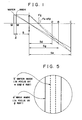
- Two objects such as a mask and a wafer are disposed, as shown in Fig.6, at respective points M and M' at an minute interval ⁇ .
- images of a mark on the mask are formed at points D and B and images of a mark on the wafer are formed at points B and C, by g and e ray, since focal lengths Fg and Fe by g ray shown with a solid line and e ray shown with a broken line are different.
- images of the marks on the mask and wafer are formed at the same point B, the image of the mark on the mask being formed by g ray and the image of the mark on the wafer being formed by e ray.
- the marks on the mask and wafer can be simultaneously viewed. Together with blurred images.
- a patten barrier filter which combines a filter for cutting off g ray and transmitting e ray and a filter for transmitting g ray and cutting off e ray is employed to remove blurred images caused due to chromatic aberration, it is possible to simultaneously observe the images of alignment marks on the mask and wafer which images lie at different positions, the point B.
- An objective for use in the present invention is the one that chromatic aberration is positively produced and various aberrations are properly compensated. Table 3 shows an example of specification of the optical system.
- a double-focus detector in which three rays of different wavelengths are employed, one for forming an image of a mask and the other two for formining an image of a wafer, will be described hereinafter.
- a general optical system is compensated in chromatic aberration, that is, achromatized, with respect to each use, so as not to cause deterioration in image formation due to a wavelength of a ray.
- chromatic aberration is compensated such that an image is not shifted with respect to two specific wavelength rays.
- Such a achromatized lens system to two wavelength rays is called an achromat.
- a focal length f of the lens L is:
- focal lengths f1 and f2 of the lenses L1 and L2 are:
- a focal length f of a compound lens system of two lenses L1 and L2 is:
- the condition of achromatization is that the resultant focal lengths with respect to e and d ray agree with each other, so that it may be set as follows.
- Equation (10) is the condition of achromatization.
- radii of curvatures of the lenses L1, L2 are eliminated as follows.
- Focal lengths f 1g and f 2g of the lenses L1 and L2 to g ray are given by the equations (4) and (5).
- n 1g and n 2g represent refractive indexes of the lenses L1 and L2 to g ray.
- the term represents the dispersion of the lens L1, represents the focal length of the lens L1 to g ray, represents the dispersion of the lens L2 and represents the focal length of the lens L2 to g ray.
- Achromatization to two rays requires at least two concave and convex lenses which have different dispersions.
- the requirement of achromatization is expressed by the equation (17).
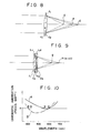
- an achromat lens system which satisfies the equation (17) is used, as shown in Fig.9, it has a focus g to g ray and another focus P at which foci to e and d ray agree wtih each other.
- chromatic aberration characteristics of an achromat lens system which satifies the equation (15) are shown with a curve A in Fig.10.
- the case of a general photographic achromatization is also shown for comparison with a curve B in Fig.10.
- a sharp image a' of a mask mark a which is in-focus to g ray and a blurred image a'' of the mask mark a which is out-of-focus to d and e ray are viewed on the outer sides and a sharp image b' of a wafer mark b which is in-focus to d and e ray and a blurred image b'' of the wafer mark b which is out-of-focus to g ray, are viewed on the inner sides.
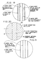
- a pattern barrier filter 10 is provided through which rays pass.
- the pattern barrier filter 10 includes its center portion II formed by a coating to transmit e and d ray and its left and right side I to transmit g ray.
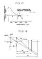
- FIG.17 A difference between Figs.17 and 10 is that while in Fig.10 a close compensation of chromatic aberration to e and d ray is made, in Fig.17 such close compensation to e and d ray is not necessarily made and a compensation of chromatic aberration is made in a scope of wavelengths ⁇ 1 to ⁇ 2 in the vicinity of e and d ray.
- an objective having characteristics shown in Fig.17 is an achromat lens having a sufficient resolution power (accomodating to N.A.) to each of a single wavelength ray (g ray shown in Fig.17) and the wavelength-band ray.
- Fig.6 which explains the principle of a double-focus lens, let it be that a single wavelength ray of g and a ray of wavelength-band ⁇ 1 to ⁇ 2 are applied to a lens having chromatic aberration characteristics showin in Fig.17.
- a focal length to a ray of wavelength-band ⁇ 1 to ⁇ 2 although, strictly speaking, there is a focal length to only two wavelength rays selected in design of an achromat lens (a large number of combinations of any two wavelengths between ⁇ 1 and ⁇ 2), it may be considered, in practice, a resolution power of a lens that according to perfomance evaluation by means of Seidel's five aberrations or a wave front aberration, for example, a focal length to a ray of wavelength-band ⁇ 1 to ⁇ 2 with a lens having characteristics shown in Fig.17 is the only one (F ⁇ 1 ⁇ 2).
- An ordinary achromat lens for use in a microscope or the like has the same focus only to two wavelength rays in the strict sense. In practice, however, by properly setteing two wavelengths to be achromatically compensated in accordance with the purpose, the same focus is realized to two wavelength rays in the vicinity of the two wavelengths properly set, that is, a wavelength-band ray.
- a lens having the same focus is practically designed to a ray of a wavelength scope ranging from 400 to 700nm which are sensitive to the naked eye.
- Table 5 shows images formed at points B, C and D shown in Fig.18.
- images are formed by a ray of wavelength-band ( ⁇ 1 to ⁇ 2).
- ⁇ 1 to ⁇ 2 configurations of alignment marks a, b of a mask and wafer are respectively a square and a rectangle which is smaller than the square, as shown in Fig.2, images at the point B would be observed as shown in Fig.19.
- a sharp image a' of a mask mark a to g ray which image is in-focus and a blurred image a'' of the mask mark a to a ray of wavelength-band ⁇ 1 to ⁇ 2 which image is out-of-focus are formed on the outer sides, and on the inner sides, are formed a sharp image b' of a wafer mark b to the ray of wavelength-band ⁇ 1 to ⁇ 2 which image is in-focus and a blurred image b'' of the wafer mark b to the g ray which image is out-of-focus.
- a pattern barrier filter 20 as shown in Fig.20 is employed.
- the filter 20 includes the center portion II formed by coating for transmitting a ray of wavelength-band ⁇ 1 to ⁇ 2 and the right and left portion I for transmitting g ray.
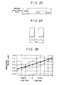
- a pattern shown in Fig.22 is normally called a WELL pattern and the configuration of its mark is as shown in Fig.23.
- an illumination ray As an illumination ray, the following four kinds of rays are selected.
- Figs.24 to 27 show respectively the following items.
- the abscissa is a reference value indicating a dimension of patterns in which a mask mark is previously shifted from a wafer mask by a pitch of 0.02 ⁇ m.
- the ordinate is a measured value indicating results measured by illuminating the reference value pattern by means of each of the rays. From Fig.27, it will be found that an accuracy of detection is improved in the following order.
- a light receiving plane such as a linear sensor
- the description is made with respect to observation by superposing a pattern barrier filter 10 or 20 on an image forming plane, it will be understood that the filter may be disposed in the optical path.
- a ray of short wave (below 500nm) may be employed.
- not being subjected to interferences or the like it may be sufficient to illuminate with a single wavelength ray.
- plural wavelength rays or wavelength-band rays are employed for illumination.
- a ray of comparatively long wavelength may be selected.
- illumination rays there are a variety of illumination rays to be assigned to a mask and a wafer.
- a combination of a superhigh pressure mercury-arc lamp and a halogen lamp may be employed, which is generally used since it is comparatively simply and ecomomically available.
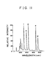
- Fig.11 is a diagram illuminating spectral distribution of a superhigh pressure mercury-arc lamp. Since bright lines of g, e and d ray are very high and have a sufficient intensity, the lamp is adapted as a light source for a single wavelength ray illumination. Consequently, the lamp is employed for a mask as a light source together with a band-pass filter for transmitting g ray (436nm). For a wafer, rays of e ray (546nm) and d ray (587nm) or halogen lamp rays are employed for a wavelength-band ray ( ⁇ 1 to ⁇ 2) illumination together with a band-pass filter for transmitting the wavelength-band ray.
- Fig.12 is a diagram, illuminating dependence of a light absorption factor on a wavelength in a lower layer resist in a multiple layer resist process when a thickness of the resist film is 2 ⁇ m ("Semiconductor World” Vol.5, 1986, Press Journal Co., Ltd. P.121).
- the absorption factor of a lower layer resist film in a multiple layer resist film is below 50% for a ray of wavelength of above 500nm.
- an absorption factor for g ray is above 90% and most of reflected rays are absorbed, resulting in that an intensity of a signal ray of a mark on a light receiving plane becomes fairly weak. Accordingly, g ray is inadequate for a light source to illuminate a wafer.
- the present invention makes it possible to reduce effects of a wafer process, to solve problems of a change in intensity of signal light interferences which are produced in a conventional contrast method, edge detection method and diffraction grating method, and to largely improve dependence on a process, thereby making an X-ray exposure apparatus highly accurate and obtaining a high throughput.
- a ray of comparatively longer wavelength is employed as a wafer mark illumination ray, in a multiple layer process which is expected to be used in more various manners with a high integration in future, an absorption factor of a lower layer resist could be reduced, so that a high reflectivity can obtained.
Landscapes
- Physics & Mathematics (AREA)
- General Physics & Mathematics (AREA)
- Exposure And Positioning Against Photoresist Photosensitive Materials (AREA)
- Lenses (AREA)
- Exposure Of Semiconductors, Excluding Electron Or Ion Beam Exposure (AREA)
Abstract
Applications Claiming Priority (1)
| Application Number | Priority Date | Filing Date | Title |
|---|---|---|---|
| PCT/JP1989/001340 WO1991010110A1 (fr) | 1989-12-28 | 1989-12-28 | Procede d'illumination en couleur composite et illumination par bandes de longueurs d'onde dans un detecteur a double foyer utilisant l'aberration chromatique |
Publications (3)
| Publication Number | Publication Date |
|---|---|
| EP0461254A1 true EP0461254A1 (fr) | 1991-12-18 |
| EP0461254A4 EP0461254A4 (en) | 1992-11-25 |
| EP0461254B1 EP0461254B1 (fr) | 1995-08-09 |
Family
ID=13959013
Family Applications (1)
| Application Number | Title | Priority Date | Filing Date |
|---|---|---|---|
| EP90900999A Expired - Lifetime EP0461254B1 (fr) | 1989-12-28 | 1989-12-28 | Procede d'illumination en couleur composite et illumination par bandes de longueurs d'onde dans un detecteur a double foyer utilisant l'aberration chromatique |
Country Status (4)
| Country | Link |
|---|---|
| US (1) | US5141322A (fr) |
| EP (1) | EP0461254B1 (fr) |
| DE (1) | DE68923802T2 (fr) |
| WO (1) | WO1991010110A1 (fr) |
Cited By (1)
| Publication number | Priority date | Publication date | Assignee | Title |
|---|---|---|---|---|
| WO2002039059A1 (fr) * | 2000-11-07 | 2002-05-16 | Cellavision Ab | Mise au point automatique |
Families Citing this family (3)
| Publication number | Priority date | Publication date | Assignee | Title |
|---|---|---|---|---|
| US7030506B2 (en) * | 2003-10-15 | 2006-04-18 | Infineon Technologies, Ag | Mask and method for using the mask in lithographic processing |
| JP2011229625A (ja) * | 2010-04-26 | 2011-11-17 | Fujifilm Corp | 内視鏡装置 |
| JP2011229603A (ja) * | 2010-04-26 | 2011-11-17 | Fujifilm Corp | 内視鏡装置 |
Family Cites Families (3)
| Publication number | Priority date | Publication date | Assignee | Title |
|---|---|---|---|---|
| JPS62140418A (ja) * | 1985-12-16 | 1987-06-24 | Canon Inc | 面位置検知装置 |
| JPS6441805A (en) * | 1987-08-07 | 1989-02-14 | Sumitomo Heavy Industries | Position detecting apparatus of two bodies, which are separated by minute distance |
| JP2699282B2 (ja) * | 1989-02-27 | 1998-01-19 | 住友重機械工業株式会社 | 色収差を利用した二重焦点検出装置 |
-
1989
- 1989-12-28 EP EP90900999A patent/EP0461254B1/fr not_active Expired - Lifetime
- 1989-12-28 US US07/651,246 patent/US5141322A/en not_active Expired - Lifetime
- 1989-12-28 DE DE68923802T patent/DE68923802T2/de not_active Expired - Fee Related
- 1989-12-28 WO PCT/JP1989/001340 patent/WO1991010110A1/fr not_active Ceased
Cited By (1)
| Publication number | Priority date | Publication date | Assignee | Title |
|---|---|---|---|---|
| WO2002039059A1 (fr) * | 2000-11-07 | 2002-05-16 | Cellavision Ab | Mise au point automatique |
Also Published As
| Publication number | Publication date |
|---|---|
| DE68923802T2 (de) | 1995-12-07 |
| DE68923802D1 (de) | 1995-09-14 |
| EP0461254B1 (fr) | 1995-08-09 |
| US5141322A (en) | 1992-08-25 |
| WO1991010110A1 (fr) | 1991-07-11 |
| EP0461254A4 (en) | 1992-11-25 |
Similar Documents
| Publication | Publication Date | Title |
|---|---|---|
| US5218193A (en) | Double-focus measurement apparatus utilizing chromatic aberration by having first and second bodies illuminated respectively by a single wavelength ray and a ray having a plurality of wavelengths | |
| US5659384A (en) | Position detection apparatus and method | |
| EP1117129A2 (fr) | Appareil d'inspection des plaquettes de semi-conducteurs | |
| US5995234A (en) | Method and apparatus for the alignment of a substrate | |
| US7894062B2 (en) | Overlay measuring method and overlay measuring apparatus using the same | |
| US4355892A (en) | Method for the projection printing | |
| JPH0786126A (ja) | パターン検出方法及びパターン検出装置及びそれを用いた投影露光装置及び露光システム | |
| US7528954B2 (en) | Method of adjusting optical imaging system, positional deviation detecting mark, method of detecting positional deviation, method of detecting position, position detecting device and mark identifying device | |
| JPS5979527A (ja) | パタ−ン検出装置 | |
| JPH0996712A (ja) | カラーフィルタの製造方法 | |
| EP0461254B1 (fr) | Procede d'illumination en couleur composite et illumination par bandes de longueurs d'onde dans un detecteur a double foyer utilisant l'aberration chromatique | |
| EP0385272B1 (fr) | Détecteur à double focalisation utilisant l'aberration chromatique | |
| JPH05119468A (ja) | マスク検査装置 | |
| JP2649391B2 (ja) | 色収差を利用した2重焦点検出装置における複色照明方法および帯域光照明方法 | |
| US4636078A (en) | Microscopic detection of membrane surface defects through interference patterns | |
| JPH06105168B2 (ja) | 薄膜パターンの検出装置 | |
| JP2961919B2 (ja) | 位置検出装置 | |
| JPH0756013A (ja) | カラーフィルター | |
| US4964146A (en) | Pattern transistor mask and method of using the same | |
| CN222213198U (zh) | 具备光路保护机构的套刻测量装置 | |
| JPH04177105A (ja) | 膜厚測定装置 | |
| JPH04102019A (ja) | 参照レティクルを用いた2重焦点装置 | |
| JP2811127B2 (ja) | 色収差2重焦点装置 | |
| KR900004051B1 (ko) | 투영노광법 및 그 장치 | |
| US10732129B2 (en) | Apparatus for and method of performing inspection and metrology process |
Legal Events
| Date | Code | Title | Description |
|---|---|---|---|
| PUAI | Public reference made under article 153(3) epc to a published international application that has entered the european phase |
Free format text: ORIGINAL CODE: 0009012 |
|
| 17P | Request for examination filed |
Effective date: 19910215 |
|
| AK | Designated contracting states |
Kind code of ref document: A1 Designated state(s): DE FR GB |
|
| A4 | Supplementary search report drawn up and despatched |
Effective date: 19921003 |
|
| AK | Designated contracting states |
Kind code of ref document: A4 Designated state(s): DE FR GB |
|
| 17Q | First examination report despatched |
Effective date: 19930722 |
|
| GRAA | (expected) grant |
Free format text: ORIGINAL CODE: 0009210 |
|
| AK | Designated contracting states |
Kind code of ref document: B1 Designated state(s): DE FR GB |
|
| PG25 | Lapsed in a contracting state [announced via postgrant information from national office to epo] |
Ref country code: FR Free format text: THE PATENT HAS BEEN ANNULLED BY A DECISION OF A NATIONAL AUTHORITY Effective date: 19950809 |
|
| REF | Corresponds to: |
Ref document number: 68923802 Country of ref document: DE Date of ref document: 19950914 |
|
| EN | Fr: translation not filed | ||
| PLBE | No opposition filed within time limit |
Free format text: ORIGINAL CODE: 0009261 |
|
| STAA | Information on the status of an ep patent application or granted ep patent |
Free format text: STATUS: NO OPPOSITION FILED WITHIN TIME LIMIT |
|
| 26N | No opposition filed | ||
| REG | Reference to a national code |
Ref country code: GB Ref legal event code: IF02 |
|
| PGFP | Annual fee paid to national office [announced via postgrant information from national office to epo] |
Ref country code: GB Payment date: 20031224 Year of fee payment: 15 |
|
| PGFP | Annual fee paid to national office [announced via postgrant information from national office to epo] |
Ref country code: DE Payment date: 20040108 Year of fee payment: 15 |
|
| PG25 | Lapsed in a contracting state [announced via postgrant information from national office to epo] |
Ref country code: GB Free format text: LAPSE BECAUSE OF NON-PAYMENT OF DUE FEES Effective date: 20041228 |
|
| PG25 | Lapsed in a contracting state [announced via postgrant information from national office to epo] |
Ref country code: DE Free format text: LAPSE BECAUSE OF NON-PAYMENT OF DUE FEES Effective date: 20050701 |
|
| GBPC | Gb: european patent ceased through non-payment of renewal fee |
Effective date: 20041228 |