EP0461928A2 - Spaltenelektrodetreiberschaltung für ein Anzeigegerät - Google Patents
Spaltenelektrodetreiberschaltung für ein Anzeigegerät Download PDFInfo
- Publication number
- EP0461928A2 EP0461928A2 EP91305429A EP91305429A EP0461928A2 EP 0461928 A2 EP0461928 A2 EP 0461928A2 EP 91305429 A EP91305429 A EP 91305429A EP 91305429 A EP91305429 A EP 91305429A EP 0461928 A2 EP0461928 A2 EP 0461928A2
- Authority
- EP
- European Patent Office
- Prior art keywords
- sample
- driving circuit
- signals
- sampling
- column electrode
- Prior art date
- Legal status (The legal status is an assumption and is not a legal conclusion. Google has not performed a legal analysis and makes no representation as to the accuracy of the status listed.)
- Granted
Links
Images


Classifications
-
- G—PHYSICS
- G09—EDUCATION; CRYPTOGRAPHY; DISPLAY; ADVERTISING; SEALS
- G09G—ARRANGEMENTS OR CIRCUITS FOR CONTROL OF INDICATING DEVICES USING STATIC MEANS TO PRESENT VARIABLE INFORMATION
- G09G3/00—Control arrangements or circuits, of interest only in connection with visual indicators other than cathode-ray tubes
- G09G3/20—Control arrangements or circuits, of interest only in connection with visual indicators other than cathode-ray tubes for presentation of an assembly of a number of characters, e.g. a page, by composing the assembly by combination of individual elements arranged in a matrix no fixed position being assigned to or needed to be assigned to the individual characters or partial characters
- G09G3/34—Control arrangements or circuits, of interest only in connection with visual indicators other than cathode-ray tubes for presentation of an assembly of a number of characters, e.g. a page, by composing the assembly by combination of individual elements arranged in a matrix no fixed position being assigned to or needed to be assigned to the individual characters or partial characters by control of light from an independent source
- G09G3/36—Control arrangements or circuits, of interest only in connection with visual indicators other than cathode-ray tubes for presentation of an assembly of a number of characters, e.g. a page, by composing the assembly by combination of individual elements arranged in a matrix no fixed position being assigned to or needed to be assigned to the individual characters or partial characters by control of light from an independent source using liquid crystals
-
- H—ELECTRICITY
- H04—ELECTRIC COMMUNICATION TECHNIQUE
- H04N—PICTORIAL COMMUNICATION, e.g. TELEVISION
- H04N3/00—Scanning details of television systems; Combination thereof with generation of supply voltages
- H04N3/10—Scanning details of television systems; Combination thereof with generation of supply voltages by means not exclusively optical-mechanical
- H04N3/12—Scanning details of television systems; Combination thereof with generation of supply voltages by means not exclusively optical-mechanical by switched stationary formation of lamps, photocells or light relays
- H04N3/127—Scanning details of television systems; Combination thereof with generation of supply voltages by means not exclusively optical-mechanical by switched stationary formation of lamps, photocells or light relays using liquid crystals
-
- G—PHYSICS
- G09—EDUCATION; CRYPTOGRAPHY; DISPLAY; ADVERTISING; SEALS
- G09G—ARRANGEMENTS OR CIRCUITS FOR CONTROL OF INDICATING DEVICES USING STATIC MEANS TO PRESENT VARIABLE INFORMATION
- G09G3/00—Control arrangements or circuits, of interest only in connection with visual indicators other than cathode-ray tubes
- G09G3/20—Control arrangements or circuits, of interest only in connection with visual indicators other than cathode-ray tubes for presentation of an assembly of a number of characters, e.g. a page, by composing the assembly by combination of individual elements arranged in a matrix no fixed position being assigned to or needed to be assigned to the individual characters or partial characters
- G09G3/34—Control arrangements or circuits, of interest only in connection with visual indicators other than cathode-ray tubes for presentation of an assembly of a number of characters, e.g. a page, by composing the assembly by combination of individual elements arranged in a matrix no fixed position being assigned to or needed to be assigned to the individual characters or partial characters by control of light from an independent source
- G09G3/36—Control arrangements or circuits, of interest only in connection with visual indicators other than cathode-ray tubes for presentation of an assembly of a number of characters, e.g. a page, by composing the assembly by combination of individual elements arranged in a matrix no fixed position being assigned to or needed to be assigned to the individual characters or partial characters by control of light from an independent source using liquid crystals
- G09G3/3611—Control of matrices with row and column drivers
- G09G3/3685—Details of drivers for data electrodes
- G09G3/3688—Details of drivers for data electrodes suitable for active matrices only
-
- G—PHYSICS
- G09—EDUCATION; CRYPTOGRAPHY; DISPLAY; ADVERTISING; SEALS
- G09G—ARRANGEMENTS OR CIRCUITS FOR CONTROL OF INDICATING DEVICES USING STATIC MEANS TO PRESENT VARIABLE INFORMATION
- G09G2310/00—Command of the display device
- G09G2310/02—Addressing, scanning or driving the display screen or processing steps related thereto
- G09G2310/0264—Details of driving circuits
- G09G2310/0297—Special arrangements with multiplexing or demultiplexing of display data in the drivers for data electrodes, in a pre-processing circuitry delivering display data to said drivers or in the matrix panel, e.g. multiplexing plural data signals to one D/A converter or demultiplexing the D/A converter output to multiple columns
-
- G—PHYSICS
- G09—EDUCATION; CRYPTOGRAPHY; DISPLAY; ADVERTISING; SEALS
- G09G—ARRANGEMENTS OR CIRCUITS FOR CONTROL OF INDICATING DEVICES USING STATIC MEANS TO PRESENT VARIABLE INFORMATION
- G09G3/00—Control arrangements or circuits, of interest only in connection with visual indicators other than cathode-ray tubes
- G09G3/20—Control arrangements or circuits, of interest only in connection with visual indicators other than cathode-ray tubes for presentation of an assembly of a number of characters, e.g. a page, by composing the assembly by combination of individual elements arranged in a matrix no fixed position being assigned to or needed to be assigned to the individual characters or partial characters
- G09G3/2007—Display of intermediate tones
- G09G3/2011—Display of intermediate tones by amplitude modulation
Definitions
- This invention relates to a column electrode driving circuit for a display apparatus, and more particularly it relates to a column electrode driving circuit for a matrix type display apparatus such as a liquid crystal display (LCD) apparatus.
- LCD liquid crystal display
- FIG. 11 An LCD apparatus is shown in Figure 11 as a typical example of a matrix type display apparatus.
- the LCD apparatus of Figure 11 comprises a liquid crystal panel 110 in which pixel electrodes 113 are arranged in a matrix, a row electrode driving circuit 115, a column electrode driving circuit 116, and a control circuit 117.
- the liquid crystal panel 110 comprises two opposing substrates, one of which has a plurality of row electrodes 111 and a plurality of column electrodes 112 intersecting the row electrodes 111.
- a transistor 114 is provided for applying a video signal to one of the pixel electrodes 113 through the corresponding column electrode 112. Namely, a plurality of the pixel electrodes 113 constituting one column are connected to one column electrode 112.
- the row electrode driving circuit 115 sequentially supplies scanning pulses to the row electrodes 111, and the column electrode driving circuit 116 supplies a video signal which is a voltage signal to be applied to the pixel electrodes 113, to the column electrodes 112.
- the row electrode driving circuit 115 supplies a scanning pulse to a certain row electrode 111
- the transistors 114 the gate of which is connected to that row electrode 111 are turned ON, and video signals on the column electrodes 112 are transmitted to the pixel electrodes 113 connected to the transistors 114 in ON state.
- the operation of the row electrode driving circuit 115 and column electrode driving circuit 116 is controlled by the control circuit 117.
- a matrix type LCD apparatus such as that shown in Figure 11 in which every pixel is provided with a transistor 114 is capable of displaying images in high contrast by means of the switching function of the transistors 114 even in cases in which multiplex drive of a plurality of row electrodes 111 is performed, and therefore it is widely used as a display unit in a portable electronic apparatus and many other electronic apparatus.
- Figure 12 shows the configuration of the column electrode driving circuit 116.
- the column electrode driving circuit 116 simultaneously processes video signals for two rows of the pixel electrodes 113 (i.e., two rows of pixels), and comprises a shift register 121, two sample-hold circuits 122A and 122B, and two output buffer circuits 123A and 123B.
- a sampling signal S input from an external unit is shifted in accordance with a clock signal ⁇ so that sampling signals q1, q2, ..., q n are sequentially output.
- the sample-hold circuit 122A samples and holds the voltage component of a video signal V A on the basis of the sampling signals q1 to q n , and outputs voltage signals QA1 to QA n .
- the other sample-hold circuit 122B samples and holds the voltage component of a video signal V B on the basis of the sampling signals q1 to q n , and outputs voltage signals QB1 to QB n .
- Each of the voltage signals QA1 to QA n and QB1 to QB n has a level which is substantially equal to the respective voltage level held in the circuits 122A and 122B.
- the output buffer circuit 123A takes in the voltage signals QA1 to QA n according to an output pulse T, and outputs them in parallel to the column electrodes 112 during the period the level of a selection signal U is positive.
- the output buffer circuit 123B takes in the voltage signals QB1 to QB n according to the output pulse T, and outputs them in parallel to the column electrodes 112 during the period the level of the selection signal U is negative.
- the operation of the column electrode driving circuit 116 will be described with reference to Figure 13.
- the video signals V A and V B are both input serially.
- the sampling signals q1, ..., q j , ..., q n are output from the shift register 121, the voltage components V Ai,l , ..., V Ai,j , ..., V Ai,n of the video signal V A are sampled and held by the sample-hold circuit 122A.
- the voltage components V Bi,l , ..., V Bi,j , ..., V Bi,n of the video signal V B are sampled and held by the sample-hold circuit 122B.
- the video signals for two rows of the pixel electrodes 113 are sampled simultaneously. Therefore, by supplying a video signal belonging to odd fields to the column electrode driving circuit 116 as the video signal V A and supplying a video signal belonging to even fields to the column electrode driving circuit 116 as the video signal V B , a display system which receives a video signal for the non-interlace scanning and uses a field memory to perform the double-speed non-interlaced display can be easily realized without increasing the frequency of the video signal.
- Figure 14 shows another LCD apparatus having a liquid crystal panel 140 in which the pixel electrodes 113 are formed into a so-called delta arrangement. More specifically, the positions of the pixel electrodes 113 in one row are shifted along the row direction by one-half pixel from those of the pixel electrodes in the adjacent rows.
- the LCD apparatus of Figure 14 having pixel electrodes with a delta arrangement is superior in display quality to the LCD apparatus of Figure 12 with a conventional arrangement of the pixel electrodes, provided that the numbers of the pixel electrodes in both the apparatus are equal to each other.
- the two sample-hold circuits 122A and 122B sample a video signal with the same sampling timing, and therefore a condition in which the sampling timing of a video signal does not conform with the position of the pixel electrode corresponding to the sampled video signal occurs every other row of the pixel electrodes 113. This causes the degradation of the display quality. For this reason, the column electrode driving circuit 116 is not suitable for driving a delta-arrangement display unit such as the panel 140.
- a device for driving a delta-arrangement display unit and having double-speed conversion means is disclosed in our copending European patent application No. 91301091.4 filed February 11, 1991.
- the column electrode driving circuit of this invention which overcomes the above-discussed and numerous other disadvantages and deficiencies of the prior art, comprises: a plurality of sample-hold means for receiving a video signal, for sampling said video signal, and for holding said sampled video signal, the sampling periods of said sample-hold means being substantially the same with each other, the sampling timings of said sample-hold means being different from each other; and output means for selecting one of said sample-hold means, and for driving said column electrodes on the basis of the sampled video signal held in said selected sample-hold means.
- the number of said sample-hold means is two.
- the sampling timings of said two sample-hold means are different from each other by one-half of said sampling period.
- said driving circuit further comprises sample signal generating means for sequentially generating sample signals, the number of said sample signals being twice the number of said column electrodes.
- one of said two sample-hold means receives the odd ones of said sample signals, and the other of said two sample-hold means receives the even ones of said sample signals, said two sample-hold means performing the sampling in accordance with said received sample signals, respectively.
- said driving circuit further comprises first and second sample signal generating means for sequentially generating sample signals, the number of said sample signals being equal to the number of said column electrodes.
- one of said two sample-hold means receives sample signals from said first sample signal generating means, and the other of said two sample-hold means receives sample signals from said second sample signal generating means.
- said driving circuit further comprises selection means coupled to the output of said sample signal generating means, and for selectively outputting either of said odd and even ones of said sample signals.
- Figure 1 is a circuit diagram illustratlng a first embodiment of the invention.
- Figure 2 is a timing chart illustrating the operation of the embodiment of Figure 1.
- Figure 3 is a circuit diagram illustrating a second embodiment of the invention.
- Figure 4 is a timing chart illustrating signals input to the embodiment of Figure 3.
- Figures 5-7 illustrate the principal portions of third to fifth embodiments of the invention, respectively.
- Figure 8 is a circuit diagram illustrating a sixth embodiment of the invention.
- Figure 9 is a timing chart illustrating the operation of the embodiment of Figure 8.
- Figure 10 is a timing chart illustrating the other possible operation of the embodiment of Figure 8.
- FIG 11 diagrammatically illustrates a conventional LCD apparatus.
- Figure 12 is a circuit diagram illustrating a column electrode driving circuit used in the LCD apparatus of Figure 11.
- Figure 13 is a timing chart illustrating the operation of the circuit of Figure 12.
- Figure 14 diagrammatically illustrates a conventional LCD apparatus with a delta-arrangement.
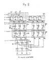
- Figure 1 shows a column electrode driving circuit according to the invention.
- the column electrode driving circuit 10 shown in Figure 1 drives the liquid crystal panel 140 ( Figure 14) with a delta arrangement, and comprises a shift register 11, two sample-hold circuits 12A and 12B, and two output buffer circuits 13A and 13B.
- the number of the stages (2n stages) of the shift register 11 is twice as that (n stages) of the shift register 121 shown in Figure 12, i.e., twice as the number of column electrodes 112 of the liquid crystal panel 140.
- the shift register 11 shifts a sampling signal S in accordance with a clock signal ⁇ D having a frequency twice that of the clock ⁇ for the shift register 121, and sequentially outputs sampling signals q1, q2, ..., q 2n .
- the sample-hold circuits 12A and 12B have the same configuration as the sample-hold circuits 122A and 122B, but the sample-hold circuit 12A samples and holds the voltage component of the video signal V A in accordance with the odd sampling signals q1, q3, ..., q 2n-1 output from the shift register 11, while the sample-hold circuit 12B samples and holds the voltage component of the video signal V B for the rows adjacent to the rows corresponding to the video signal V A in accordance with the even sampling signals q2, q4, ..., q 2n output from the shift register 11.
- the output buffer circuit 13A simultaneously takes in the voltage signals QA1 to QA n which are substantially equal to the voltage held by the sample-hold circuit 12A, in accordance with the output pulse T, and outputs them in parallel to the column electrodes 112 during the period the level of the selection signal U is positive.
- the output buffer 13B simultaneously takes in the voltage signals QB1 to QB n which are substantially equal to the voltage held by the sample-hold circuit 12B, in accordance with the output pulse T, and outputs them in parallel to the column electrodes 112 during the period the level of the selection signal U is negative.
- the operation of the column electrode driving circuit 10 will be described in more detail with reference to Figure 2.
- Both video signals V A and V B are input serially.
- the sample-hold circuit 12A samples the voltage components V Ai,1 , ..., V Ai,2j-1 , ..., V Ai,2n-1 (corresponding to the ith row of the pixel electrodes 113) of the video signal V A at the timings the odd sampling signals q1, ...q 2j-1 , ... q 2n-1 are output from the shift register 11.
- the sample-hold circuit 12B samples the voltage components V Bi+1,2 , ..., V Bi+1,2j , ..., V Bi+1,2n (corresponding to the (i+1)th row of the pixel electrodes 113) of the video signal V B at the timings the even sampling signals are output from the shift register 11.
- the voltage signals QA j are output from the output buffer circuit 13A as voltage signals Q j during the selection signal U in the first half of the next sampling period (for the (i+2)th and (i+3)th rows) is positive.
- Both the sampling period of the sample-hold circuit 12A and that of the sample-hold circuit 12B are one-half of the period of the clock signal ⁇ D .
- the sampling timing of the sample-hold circuit 12B is delayed behind that of the sample-hold circuit 12A by one-half of the above sampling period. According to this embodiment, therefore, the sampling of a video signal is performed in conformity with a delta arrangement, and therefore the liquid crystal panel 140 with a delta arrangement can be driven with an excellent image quality.
- video signals for two rows of pixel electrodes 113 are sampled simultaneously in one sampling period, and the thus sampled video signals are then used to drive the column electrodes 112 in the time division manner in the next sampling period. Therefore, the display quality equivalent to that of the double-speed conversion display can be achieved without using an external double-speed converter for a video signal.
- Figure 3 shows the principal components of a second embodiment of the invention.
- this embodiment is provided with two shift registers 31A and 31B.
- the number (n) of stages of each of the shift registers 31A and 31B is equal to the number (n) of column electrodes 112 of the liquid crystal panel 140.
- the shift register 31A receives a first clock signal ⁇ A , and a first sampling signal S A
- the shift register 31B receives a second clock signal ⁇ B , and a second sampling signal S B .
- the first and second clock signals ⁇ A and ⁇ B have the same frequency, but the phase of the clock signal ⁇ B is shifted from that of the clock signal ⁇ A by one-half of the clock period as shown in Figure 4.
- the second sampling signal S B is delayed by one pulse width from the first sampling signal S A .
- the shift register 31A shifts the sampling signal S A in accordance with the clock signal ⁇ A , and sequentially outputs the sampling signals qA1 to qA n to the sample-hold circuit 12A.
- the shift register 31B shifts the sampling signal S B according to the clock signal ⁇ B which has the same period as the clock signal ⁇ A , and sequentially outputs the sampling signals qB1 to qB n to the sample-hold circuit 12B.
- the phase of the clock signal ⁇ B differs from that of the clock signal ⁇ A by one-half of the clock period, and hence the sampling timing of the sample-hold circuit 12B differs from that of the sample-hold circuit 12A by one-half of the sampling period (equal to the clock period). Therefore, this embodiment can achieve the same results as the column electrode driving circuit 10 of Figure 1.
- Figure 5 shows the principal components of a third embodiment of the invention.
- function switching circuits 541 to 54 n are provided at the output of the shift register 11, whereby the same operation as that of the column electrode driving circuit 116 ( Figure 12) can be achieved.
- Each of the function switching circuits 541 to 54 n receives two sampling signals q 2j-1 and q 2j , and a function switching signal D, and comprises two AND gates 541 and 542, an OR gate 543, and an inverter 544.
- the function switching circuits 541 to 54 n generate sampling signals q2′ to q 2n ′ which are supplied to the sample-hold circuit 12B ( Figure 1), respectively.
- the sampling signal q2′ which is generated by the first function switching circuit 541 corresponding to the sampling signals q1 ant q2 is equivalent to the sampling signal q1 when the function switching signal D is HIGH, and is equivalent to the sampling signal q2 when the function switching signal D is LOW.
- this embodiment functions in the same manner as the column electrode driving circuit 116 ( Figure 12), and when the function switching signal D is LOW, this embodiment functions in the same manner as the column electrode driving circuit 10 of Figure 1.
- Figure 6 shows the principal parts of a fourth embodiment of the invention.
- the sample-hold circuits 12A and 12B sample the same input video signal V.
- the sampling timings of the two sample-hold circuits 12A and 12B differ by one-half of the sampling period, and therefore the number of the sampling points for the video signal V is twice as compared that in the column electrode driving circuit 116 ( Figure 12).
- the writing is performed at double speed in this way for two rows of pixels in a liquid crystal panel with a delta arrangement, based on the sampled video signal, resulting in that resolution is improved and slanted lines are displayed linearly.
- it is advantageous to sample the same video signal V while there is no advantage for the two sample-hold circuits 122A and 122B to sample the same video signal in the column electrode driving circuit 116 ( Figure 12).
- Figure 7 shows the principal parts of a fifth embodiment of the invention.
- the fifth embodiment is provided with an output buffer circuit 73 which comprises holding sections 731A and 731B, selection sections 732A and 732B and a common buffer section 733 for the signals from the sample-hold circuits 12A and 12B.
- the holding section 731A holds the voltage signals QA1 to QA n transmitted from the sample-hold circuit 12A
- the holding section 731B holds the voltage signals QB1 to QB n transmitted from the sample-hold circuit 12B.
- the selection section 732A transmits the signals held by the holding section 731A to the buffer section 733 when the selection signal U is positive.
- the selection section 732B transmits the signals held by the holding section 731B to the buffer section 733 when the selection signal U is negative.
- FIG. 8 A sixth embodiment of the invention is shown in Figure 8.
- This embodiment has two shift registers 81A and 81B each of which comprises D-type flip-flops 811 connected in series.
- the sampling signal S is supplied to the D input of the first D-type flip-flops 811 of the shift registers 81A and 81B.
- a clock signal ⁇ with a duty ratio of 50% is supplied to the CK input of the D-type flip-flops of the shift register 81A.
- the output of an XOR gate 87 to which the clock signal ⁇ and a function selection signal D are input is supplied to the CK input of the D-type flip-flops of the other shift register 81B.
- the sampling signals output from the shift registers 81A and 81B may have a pulse width longer than the sampling period ts, so that the sampling timing of sample-hold circuits 82A and 82B (which will be described below) can be shifted one-half of the sampling period (i.e., ts/2).
- the sample-hold circuit 82A comprises analog switches 821 and sampling capacitors 822.
- the analog switches 821 close according to the corresponding sampling signal from the shift register 81A, thereby supplying the input video signal V A to the sampling capacitor 822. If the time required to charge the sampling capacitor 822 is sufficiently shorter than the sampling period ts, then the voltage of the video signal V A at the fall edge of each of the sampling signals qA1, ... is held in the corresponding sampling capacitor 822.
- the sample-hold circuit 82B has the same configuration as the sample-hold circuit 82A, but it samples and holds the video signal V B according to the sampling signals qB1, ... output from the shift register 81B.
- the sampling points of the video signals V A and V B are shown in Figure 9.
- the outputs of the sample-hold circuits 82A and 82B are input to holding circuits 83A and 83B, respectively.
- the holding circuit 83A comprises analog switches 831 and holding capacitors 832.
- the analog switches 831 close in accordance with the output pulse T, so that the voltages held in the sampling capacitors 822 of the sample-hold circuit 82A are simultaneously transmitted to the holding capacitors 832.
- This transmission of voltages from the sampling capacitors 822 to the holding capacitors 832 is performed during the period in which the sample-hold circuit 82A is inhibited from sampling (e.g., the horizontal blanking period in a television signal).
- the holding circuit 83B has the same configuration as the holding circuit 83A, and the voltages held by the sample-hold circuit 82B are transmitted to the holding circuit 83B according to the output pulse T.
- the outputs QA1, ... and QB1, ... of the holding circuits 83A and 83B are supplied to an output selection circuit 84.
- the output selection circuit 84 has analog switches 841 which selectively output either the outputs of the holding circuit 83A or those of the holding circuit 83B according to the selection signal U.
- the outputs from the output selection circuit 84 are transmitted to the column electrodes 112 of the liquid crystal panel 140 via the buffer circuit 85.
- the Invention are generally directed to column elect:ode driving circuits having a plurality of sample-hold circuits in which the sampling timings of the sample-hold circuits differ from each other.
- the column electrode driving circuit can drive a display apparatus which has a delta arrangement display unit, with an excellent image quality.
- the video signals for two rows in the display unit can be processed simultaneously by two sample-hold means with sampling timings which differ mutually by one-half of the sampling period. Therefore, a high quality display which is equivalent to a double-speed conversion display can be performed without providing external double-speed conversion means or a line memory or frame memory for a video signal.
Landscapes
- Engineering & Computer Science (AREA)
- Chemical & Material Sciences (AREA)
- Crystallography & Structural Chemistry (AREA)
- Physics & Mathematics (AREA)
- Computer Hardware Design (AREA)
- General Physics & Mathematics (AREA)
- Theoretical Computer Science (AREA)
- Multimedia (AREA)
- Signal Processing (AREA)
- Liquid Crystal Display Device Control (AREA)
- Transforming Electric Information Into Light Information (AREA)
- Control Of Indicators Other Than Cathode Ray Tubes (AREA)
Applications Claiming Priority (2)
| Application Number | Priority Date | Filing Date | Title |
|---|---|---|---|
| JP156263/90 | 1990-06-14 | ||
| JP2156263A JP2892444B2 (ja) | 1990-06-14 | 1990-06-14 | 表示装置の列電極駆動回路 |
Publications (3)
| Publication Number | Publication Date |
|---|---|
| EP0461928A2 true EP0461928A2 (de) | 1991-12-18 |
| EP0461928A3 EP0461928A3 (en) | 1993-01-13 |
| EP0461928B1 EP0461928B1 (de) | 1997-05-21 |
Family
ID=15623984
Family Applications (1)
| Application Number | Title | Priority Date | Filing Date |
|---|---|---|---|
| EP91305429A Expired - Lifetime EP0461928B1 (de) | 1990-06-14 | 1991-06-14 | Spaltenelektrodetreiberschaltung für ein Anzeigegerät |
Country Status (5)
| Country | Link |
|---|---|
| US (1) | US5602561A (de) |
| EP (1) | EP0461928B1 (de) |
| JP (1) | JP2892444B2 (de) |
| KR (1) | KR950010135B1 (de) |
| DE (1) | DE69126171T2 (de) |
Cited By (5)
| Publication number | Priority date | Publication date | Assignee | Title |
|---|---|---|---|---|
| EP0572250A1 (de) * | 1992-05-27 | 1993-12-01 | Kabushiki Kaisha Toshiba | Steuersystem für eine Flüssigkristallanzeigevorrichtung |
| EP0565167A3 (en) * | 1992-04-07 | 1993-12-08 | Philips Electronics Uk Ltd | Multi-standard video matrix display apparatus and its method of operation |
| EP0637009A3 (de) * | 1993-07-30 | 1997-03-19 | Canon Kk | Steuerverfahren und Vorrichtung für eine Flüssigkristallfarbanzeige mit aktiver Matrix. |
| GB2323958A (en) * | 1997-04-04 | 1998-10-07 | Sharp Kk | Active matrix devices |
| EP1096467A3 (de) * | 1999-11-01 | 2002-01-02 | Sharp Kabushiki Kaisha | Schieberegister und Bildanzeigegerät |
Families Citing this family (24)
| Publication number | Priority date | Publication date | Assignee | Title |
|---|---|---|---|---|
| TW270198B (de) | 1994-06-21 | 1996-02-11 | Hitachi Seisakusyo Kk | |
| US5883609A (en) * | 1994-10-27 | 1999-03-16 | Nec Corporation | Active matrix type liquid crystal display with multi-media oriented drivers and driving method for same |
| JP3520131B2 (ja) * | 1995-05-15 | 2004-04-19 | 株式会社東芝 | 液晶表示装置 |
| JP3148972B2 (ja) * | 1995-06-01 | 2001-03-26 | キヤノン株式会社 | カラー表示装置の駆動回路 |
| US5798747A (en) * | 1995-11-17 | 1998-08-25 | National Semiconductor Corporation | Methods and apparatuses for high-speed video sample and hold amplification for analog flat panel display |
| JP2792490B2 (ja) * | 1995-12-20 | 1998-09-03 | 日本電気株式会社 | 液晶表示装置用駆動回路のサンプルホールド回路 |
| JP3330812B2 (ja) * | 1996-03-22 | 2002-09-30 | シャープ株式会社 | マトリックス型表示装置およびその駆動方法 |
| US5828357A (en) * | 1996-03-27 | 1998-10-27 | Sharp Kabushiki Kaisha | Display panel driving method and display apparatus |
| US5781167A (en) * | 1996-04-04 | 1998-07-14 | Northrop Grumman Corporation | Analog video input flat panel display interface |
| JP3516323B2 (ja) * | 1996-05-23 | 2004-04-05 | シャープ株式会社 | シフトレジスタ回路および画像表示装置 |
| JP2923906B2 (ja) * | 1996-06-07 | 1999-07-26 | 日本電気株式会社 | 液晶表示装置の駆動回路 |
| JPH10153986A (ja) * | 1996-09-25 | 1998-06-09 | Toshiba Corp | 表示装置 |
| TW373115B (en) * | 1997-02-07 | 1999-11-01 | Hitachi Ltd | Liquid crystal display device |
| JPH117268A (ja) * | 1997-06-18 | 1999-01-12 | Sony Corp | サンプルホールド回路 |
| KR100430100B1 (ko) * | 1999-03-06 | 2004-05-03 | 엘지.필립스 엘시디 주식회사 | 액정표시장치의 구동방법 |
| JP3589926B2 (ja) * | 2000-02-02 | 2004-11-17 | シャープ株式会社 | シフトレジスタ回路および画像表示装置 |
| JP2003022058A (ja) * | 2001-07-09 | 2003-01-24 | Seiko Epson Corp | 電気光学装置、電気光学装置の駆動回路、電気光学装置の駆動方法および電子機器 |
| KR100815897B1 (ko) * | 2001-10-13 | 2008-03-21 | 엘지.필립스 엘시디 주식회사 | 액정표시장치의 데이터 구동 장치 및 방법 |
| JP4175058B2 (ja) * | 2002-08-27 | 2008-11-05 | セイコーエプソン株式会社 | 表示駆動回路及び表示装置 |
| JP2004177433A (ja) * | 2002-11-22 | 2004-06-24 | Sharp Corp | シフトレジスタブロック、それを備えたデータ信号線駆動回路及び表示装置 |
| JP2004309822A (ja) * | 2003-04-08 | 2004-11-04 | Sony Corp | 表示装置 |
| US8866707B2 (en) * | 2005-03-31 | 2014-10-21 | Semiconductor Energy Laboratory Co., Ltd. | Display device, and apparatus using the display device having a polygonal pixel electrode |
| KR20090006198A (ko) * | 2006-04-19 | 2009-01-14 | 이그니스 이노베이션 인크. | 능동형 디스플레이를 위한 안정적 구동 방식 |
| JP2012256012A (ja) * | 2010-09-15 | 2012-12-27 | Semiconductor Energy Lab Co Ltd | 表示装置 |
Family Cites Families (10)
| Publication number | Priority date | Publication date | Assignee | Title |
|---|---|---|---|---|
| JPS5741078A (en) * | 1980-08-22 | 1982-03-06 | Seiko Epson Corp | Synchronizing circuit of matrix television |
| JPS57201295A (en) * | 1981-06-04 | 1982-12-09 | Sony Corp | Two-dimensional address device |
| JPS6249399A (ja) * | 1985-08-29 | 1987-03-04 | キヤノン株式会社 | 表示装置 |
| EP0287055B1 (de) * | 1987-04-15 | 1993-09-29 | Sharp Kabushiki Kaisha | Flüssigkristallanzeigegerät |
| JPS63285593A (ja) * | 1987-05-18 | 1988-11-22 | シャープ株式会社 | 液晶表示装置 |
| GB2205191A (en) * | 1987-05-29 | 1988-11-30 | Philips Electronic Associated | Active matrix display system |
| JPH0654421B2 (ja) * | 1987-12-07 | 1994-07-20 | シャープ株式会社 | マトリクス型液晶表示装置の列電極駆動回路 |
| JPH0283584A (ja) * | 1988-09-21 | 1990-03-23 | Hitachi Ltd | 倍速線順次走査回路 |
| JPH02157813A (ja) * | 1988-12-12 | 1990-06-18 | Sharp Corp | 液晶表示パネル |
| US5041823A (en) * | 1988-12-29 | 1991-08-20 | Honeywell Inc. | Flicker-free liquid crystal display driver system |
-
1990
- 1990-06-14 JP JP2156263A patent/JP2892444B2/ja not_active Expired - Lifetime
-
1991
- 1991-06-14 EP EP91305429A patent/EP0461928B1/de not_active Expired - Lifetime
- 1991-06-14 KR KR1019910009893A patent/KR950010135B1/ko not_active Expired - Lifetime
- 1991-06-14 DE DE69126171T patent/DE69126171T2/de not_active Expired - Fee Related
-
1993
- 1993-11-08 US US08/148,408 patent/US5602561A/en not_active Expired - Lifetime
Cited By (11)
| Publication number | Priority date | Publication date | Assignee | Title |
|---|---|---|---|---|
| EP0565167A3 (en) * | 1992-04-07 | 1993-12-08 | Philips Electronics Uk Ltd | Multi-standard video matrix display apparatus and its method of operation |
| US5335023A (en) * | 1992-04-07 | 1994-08-02 | U.S. Philips Corporation | Multi-standard video matrix display apparatus and its method of operation |
| EP0572250A1 (de) * | 1992-05-27 | 1993-12-01 | Kabushiki Kaisha Toshiba | Steuersystem für eine Flüssigkristallanzeigevorrichtung |
| US5745093A (en) * | 1992-05-27 | 1998-04-28 | Kabushiki Kaisha Toshiba | Liquid crystal display driving system |
| EP0637009A3 (de) * | 1993-07-30 | 1997-03-19 | Canon Kk | Steuerverfahren und Vorrichtung für eine Flüssigkristallfarbanzeige mit aktiver Matrix. |
| US5619225A (en) * | 1993-07-30 | 1997-04-08 | Canon Kabushiki Kaisha | Liquid crystal display apparatus and method of driving the same |
| GB2323958A (en) * | 1997-04-04 | 1998-10-07 | Sharp Kk | Active matrix devices |
| US6437767B1 (en) | 1997-04-04 | 2002-08-20 | Sharp Kabushiki Kaisha | Active matrix devices |
| EP1096467A3 (de) * | 1999-11-01 | 2002-01-02 | Sharp Kabushiki Kaisha | Schieberegister und Bildanzeigegerät |
| US6724361B1 (en) | 1999-11-01 | 2004-04-20 | Sharp Kabushiki Kaisha | Shift register and image display device |
| US7212184B2 (en) | 1999-11-01 | 2007-05-01 | Sharp Kabushiki Kaisha | Shift register and image display device |
Also Published As
| Publication number | Publication date |
|---|---|
| KR950010135B1 (ko) | 1995-09-07 |
| DE69126171T2 (de) | 1997-11-20 |
| US5602561A (en) | 1997-02-11 |
| DE69126171D1 (de) | 1997-06-26 |
| JPH0450895A (ja) | 1992-02-19 |
| EP0461928A3 (en) | 1993-01-13 |
| EP0461928B1 (de) | 1997-05-21 |
| KR920001420A (ko) | 1992-01-30 |
| JP2892444B2 (ja) | 1999-05-17 |
Similar Documents
| Publication | Publication Date | Title |
|---|---|---|
| EP0461928A2 (de) | Spaltenelektrodetreiberschaltung für ein Anzeigegerät | |
| US5748175A (en) | LCD driving apparatus allowing for multiple aspect resolution | |
| US5122790A (en) | Liquid crystal projection apparatus and driving method thereof | |
| EP0852372B1 (de) | Bildanzeigevorrichtung | |
| US4694349A (en) | Liquid crystal matrix display panel driver circuit | |
| US20010013852A1 (en) | Liquid crystal display device | |
| US7050034B2 (en) | Display apparatus | |
| US5990979A (en) | Gamma correction circuit and video display apparatus using the same | |
| JP2747583B2 (ja) | 液晶パネルの駆動回路及び液晶装置 | |
| US6020873A (en) | Liquid crystal display apparatus with arbitrary magnification of displayed image | |
| JPH02210985A (ja) | マトリクス型液晶表示装置の駆動回路 | |
| EP0449508B1 (de) | Steuereinrichtung für eine Flüssigkristallanzeige | |
| JPH0546123A (ja) | 液晶駆動装置 | |
| JPH09325738A (ja) | 液晶ディスプレイ装置とその駆動方法 | |
| KR100795985B1 (ko) | 능동 매트릭스 디스플레이용 픽셀 샘플링 회로 | |
| KR100256974B1 (ko) | 멀티 스캔 장치 | |
| JPH05210086A (ja) | 画像表示装置の駆動方法 | |
| KR100304867B1 (ko) | 주사방식의가변이가능한액정표시장치 | |
| JPH0628863Y2 (ja) | 液晶表示装置 | |
| JPH02143298A (ja) | 液晶ディスプレイ装置 | |
| JPH043195A (ja) | マトリクス型画像表示装置の駆動方法 | |
| JPH0616223B2 (ja) | 倍速線順次走査回路 | |
| JPH05108028A (ja) | インターレース走査回路 | |
| JPH10268840A (ja) | 液晶表示装置 | |
| JPH03196780A (ja) | アクティブマトリクス液晶ディスプレイ駆動装置 |
Legal Events
| Date | Code | Title | Description |
|---|---|---|---|
| PUAI | Public reference made under article 153(3) epc to a published international application that has entered the european phase |
Free format text: ORIGINAL CODE: 0009012 |
|
| AK | Designated contracting states |
Kind code of ref document: A2 Designated state(s): DE FR GB IT NL |
|
| PUAL | Search report despatched |
Free format text: ORIGINAL CODE: 0009013 |
|
| AK | Designated contracting states |
Kind code of ref document: A3 Designated state(s): DE FR GB IT NL |
|
| 17P | Request for examination filed |
Effective date: 19930315 |
|
| 17Q | First examination report despatched |
Effective date: 19941004 |
|
| GRAG | Despatch of communication of intention to grant |
Free format text: ORIGINAL CODE: EPIDOS AGRA |
|
| GRAH | Despatch of communication of intention to grant a patent |
Free format text: ORIGINAL CODE: EPIDOS IGRA |
|
| GRAH | Despatch of communication of intention to grant a patent |
Free format text: ORIGINAL CODE: EPIDOS IGRA |
|
| GRAH | Despatch of communication of intention to grant a patent |
Free format text: ORIGINAL CODE: EPIDOS IGRA |
|
| GRAA | (expected) grant |
Free format text: ORIGINAL CODE: 0009210 |
|
| AK | Designated contracting states |
Kind code of ref document: B1 Designated state(s): DE FR GB IT NL |
|
| ITF | It: translation for a ep patent filed | ||
| REF | Corresponds to: |
Ref document number: 69126171 Country of ref document: DE Date of ref document: 19970626 |
|
| ET | Fr: translation filed | ||
| PLBE | No opposition filed within time limit |
Free format text: ORIGINAL CODE: 0009261 |
|
| STAA | Information on the status of an ep patent application or granted ep patent |
Free format text: STATUS: NO OPPOSITION FILED WITHIN TIME LIMIT |
|
| 26N | No opposition filed | ||
| PGFP | Annual fee paid to national office [announced via postgrant information from national office to epo] |
Ref country code: DE Payment date: 20010605 Year of fee payment: 11 |
|
| PGFP | Annual fee paid to national office [announced via postgrant information from national office to epo] |
Ref country code: FR Payment date: 20010611 Year of fee payment: 11 |
|
| PGFP | Annual fee paid to national office [announced via postgrant information from national office to epo] |
Ref country code: GB Payment date: 20010613 Year of fee payment: 11 |
|
| PGFP | Annual fee paid to national office [announced via postgrant information from national office to epo] |
Ref country code: NL Payment date: 20010628 Year of fee payment: 11 |
|
| REG | Reference to a national code |
Ref country code: GB Ref legal event code: IF02 |
|
| PG25 | Lapsed in a contracting state [announced via postgrant information from national office to epo] |
Ref country code: GB Free format text: LAPSE BECAUSE OF NON-PAYMENT OF DUE FEES Effective date: 20020614 |
|
| PG25 | Lapsed in a contracting state [announced via postgrant information from national office to epo] |
Ref country code: NL Free format text: LAPSE BECAUSE OF NON-PAYMENT OF DUE FEES Effective date: 20030101 Ref country code: DE Free format text: LAPSE BECAUSE OF NON-PAYMENT OF DUE FEES Effective date: 20030101 |
|
| GBPC | Gb: european patent ceased through non-payment of renewal fee |
Effective date: 20020614 |
|
| PG25 | Lapsed in a contracting state [announced via postgrant information from national office to epo] |
Ref country code: FR Free format text: LAPSE BECAUSE OF NON-PAYMENT OF DUE FEES Effective date: 20030228 |
|
| NLV4 | Nl: lapsed or anulled due to non-payment of the annual fee |
Effective date: 20030101 |
|
| REG | Reference to a national code |
Ref country code: FR Ref legal event code: ST |
|
| PG25 | Lapsed in a contracting state [announced via postgrant information from national office to epo] |
Ref country code: IT Free format text: LAPSE BECAUSE OF NON-PAYMENT OF DUE FEES;WARNING: LAPSES OF ITALIAN PATENTS WITH EFFECTIVE DATE BEFORE 2007 MAY HAVE OCCURRED AT ANY TIME BEFORE 2007. THE CORRECT EFFECTIVE DATE MAY BE DIFFERENT FROM THE ONE RECORDED. Effective date: 20050614 |