EP0463763A2 - Halbleiterpackung und Verfahren mit Rundummetallisierung - Google Patents
Halbleiterpackung und Verfahren mit Rundummetallisierung Download PDFInfo
- Publication number
- EP0463763A2 EP0463763A2 EP91305223A EP91305223A EP0463763A2 EP 0463763 A2 EP0463763 A2 EP 0463763A2 EP 91305223 A EP91305223 A EP 91305223A EP 91305223 A EP91305223 A EP 91305223A EP 0463763 A2 EP0463763 A2 EP 0463763A2
- Authority
- EP
- European Patent Office
- Prior art keywords
- shelf
- metallization
- chip
- bonding
- peripheral edge
- Prior art date
- Legal status (The legal status is an assumption and is not a legal conclusion. Google has not performed a legal analysis and makes no representation as to the accuracy of the status listed.)
- Withdrawn
Links
Images

Classifications
-
- H—ELECTRICITY
- H10—SEMICONDUCTOR DEVICES; ELECTRIC SOLID-STATE DEVICES NOT OTHERWISE PROVIDED FOR
- H10W—GENERIC PACKAGES, INTERCONNECTIONS, CONNECTORS OR OTHER CONSTRUCTIONAL DETAILS OF DEVICES COVERED BY CLASS H10
- H10W70/00—Package substrates; Interposers; Redistribution layers [RDL]
- H10W70/60—Insulating or insulated package substrates; Interposers; Redistribution layers
- H10W70/62—Insulating or insulated package substrates; Interposers; Redistribution layers characterised by their interconnections
- H10W70/65—Shapes or dispositions of interconnections
- H10W70/657—Shapes or dispositions of interconnections on sidewalls or bottom surfaces of the package substrates, interposers or redistribution layers
-
- H—ELECTRICITY
- H10—SEMICONDUCTOR DEVICES; ELECTRIC SOLID-STATE DEVICES NOT OTHERWISE PROVIDED FOR
- H10W—GENERIC PACKAGES, INTERCONNECTIONS, CONNECTORS OR OTHER CONSTRUCTIONAL DETAILS OF DEVICES COVERED BY CLASS H10
- H10W70/00—Package substrates; Interposers; Redistribution layers [RDL]
- H10W70/60—Insulating or insulated package substrates; Interposers; Redistribution layers
- H10W70/67—Insulating or insulated package substrates; Interposers; Redistribution layers characterised by their insulating layers or insulating parts
- H10W70/68—Shapes or dispositions thereof
-
- H—ELECTRICITY
- H10—SEMICONDUCTOR DEVICES; ELECTRIC SOLID-STATE DEVICES NOT OTHERWISE PROVIDED FOR
- H10W—GENERIC PACKAGES, INTERCONNECTIONS, CONNECTORS OR OTHER CONSTRUCTIONAL DETAILS OF DEVICES COVERED BY CLASS H10
- H10W70/00—Package substrates; Interposers; Redistribution layers [RDL]
- H10W70/60—Insulating or insulated package substrates; Interposers; Redistribution layers
- H10W70/67—Insulating or insulated package substrates; Interposers; Redistribution layers characterised by their insulating layers or insulating parts
- H10W70/68—Shapes or dispositions thereof
- H10W70/685—Shapes or dispositions thereof comprising multiple insulating layers
-
- H—ELECTRICITY
- H10—SEMICONDUCTOR DEVICES; ELECTRIC SOLID-STATE DEVICES NOT OTHERWISE PROVIDED FOR
- H10W—GENERIC PACKAGES, INTERCONNECTIONS, CONNECTORS OR OTHER CONSTRUCTIONAL DETAILS OF DEVICES COVERED BY CLASS H10
- H10W72/00—Interconnections or connectors in packages
- H10W72/50—Bond wires
-
- H—ELECTRICITY
- H10—SEMICONDUCTOR DEVICES; ELECTRIC SOLID-STATE DEVICES NOT OTHERWISE PROVIDED FOR
- H10W—GENERIC PACKAGES, INTERCONNECTIONS, CONNECTORS OR OTHER CONSTRUCTIONAL DETAILS OF DEVICES COVERED BY CLASS H10
- H10W70/00—Package substrates; Interposers; Redistribution layers [RDL]
- H10W70/60—Insulating or insulated package substrates; Interposers; Redistribution layers
- H10W70/67—Insulating or insulated package substrates; Interposers; Redistribution layers characterised by their insulating layers or insulating parts
- H10W70/68—Shapes or dispositions thereof
- H10W70/682—Shapes or dispositions thereof comprising holes having chips therein
-
- H—ELECTRICITY
- H10—SEMICONDUCTOR DEVICES; ELECTRIC SOLID-STATE DEVICES NOT OTHERWISE PROVIDED FOR
- H10W—GENERIC PACKAGES, INTERCONNECTIONS, CONNECTORS OR OTHER CONSTRUCTIONAL DETAILS OF DEVICES COVERED BY CLASS H10
- H10W72/00—Interconnections or connectors in packages
- H10W72/071—Connecting or disconnecting
- H10W72/075—Connecting or disconnecting of bond wires
- H10W72/07551—Connecting or disconnecting of bond wires characterised by changes in properties of the bond wires during the connecting
- H10W72/07554—Connecting or disconnecting of bond wires characterised by changes in properties of the bond wires during the connecting changes in dispositions
-
- H—ELECTRICITY
- H10—SEMICONDUCTOR DEVICES; ELECTRIC SOLID-STATE DEVICES NOT OTHERWISE PROVIDED FOR
- H10W—GENERIC PACKAGES, INTERCONNECTIONS, CONNECTORS OR OTHER CONSTRUCTIONAL DETAILS OF DEVICES COVERED BY CLASS H10
- H10W72/00—Interconnections or connectors in packages
- H10W72/50—Bond wires
- H10W72/531—Shapes of wire connectors
- H10W72/536—Shapes of wire connectors the connected ends being ball-shaped
-
- H—ELECTRICITY
- H10—SEMICONDUCTOR DEVICES; ELECTRIC SOLID-STATE DEVICES NOT OTHERWISE PROVIDED FOR
- H10W—GENERIC PACKAGES, INTERCONNECTIONS, CONNECTORS OR OTHER CONSTRUCTIONAL DETAILS OF DEVICES COVERED BY CLASS H10
- H10W72/00—Interconnections or connectors in packages
- H10W72/50—Bond wires
- H10W72/531—Shapes of wire connectors
- H10W72/5363—Shapes of wire connectors the connected ends being wedge-shaped
-
- H—ELECTRICITY
- H10—SEMICONDUCTOR DEVICES; ELECTRIC SOLID-STATE DEVICES NOT OTHERWISE PROVIDED FOR
- H10W—GENERIC PACKAGES, INTERCONNECTIONS, CONNECTORS OR OTHER CONSTRUCTIONAL DETAILS OF DEVICES COVERED BY CLASS H10
- H10W72/00—Interconnections or connectors in packages
- H10W72/50—Bond wires
- H10W72/541—Dispositions of bond wires
- H10W72/547—Dispositions of multiple bond wires
-
- H—ELECTRICITY
- H10—SEMICONDUCTOR DEVICES; ELECTRIC SOLID-STATE DEVICES NOT OTHERWISE PROVIDED FOR
- H10W—GENERIC PACKAGES, INTERCONNECTIONS, CONNECTORS OR OTHER CONSTRUCTIONAL DETAILS OF DEVICES COVERED BY CLASS H10
- H10W90/00—Package configurations
- H10W90/701—Package configurations characterised by the relative positions of pads or connectors relative to package parts
- H10W90/751—Package configurations characterised by the relative positions of pads or connectors relative to package parts of bond wires
- H10W90/754—Package configurations characterised by the relative positions of pads or connectors relative to package parts of bond wires between a chip and a stacked insulating package substrate, interposer or RDL
Definitions
- This invention pertains generally to semiconductor devices and, more particularly, to the packaging of a semiconductor chip or die.
- a common type of plastic pin grid array (PPGA) package heretofore provided is similar in construction to printed wiring boards, the main difference being that the package has a cavity in the middle, with a series of shelves carrying various package layers and traces for wire bonding to a chip.
- PPGA plastic pin grid array
- an entire layer on a bonding shelf generally has to be dedicated to that particular voltage.
- An example of a package of this type is illustrated in Figure 1.
- the package illustrated in Figure 1 has a series of three bonding shelves or tiers designated by the reference numerals 11, 12 and 13 surrounding a die or chip 14. Each of these shelves has a layer of metallization on its upper surface to which a one or more leads 16 from the chip is attached.
- the metallization layer on the middle shelf 12 carries the supply voltage V CC , and the entire shelf is dedicated to this particular voltage. There are no other bonding pads or leads on this shelf.
- the supply voltage V CC is carried by a metallization layer 17 on the under side of a bonding shelf 18, and connections to this layer are made through a series of vias 19 passing through the shelf. Leads 21 connected to other bonding pads on the shelf extend beyond the vias and have substantially more inductance than is generally desired.
- connections with a metalliaation layer on the under side of a bonding shelf are made by one or more conductive fingers or traces which extend between the upper and lower sides of the shelf at the edge of the opening in which the die is mounted.
- the invention provides an improved semiconductor package and method in which a cavity is provided for the chip or die, a bonding shelf extends peripherally of the cavity, and a layer of metallization extends along the under side of the shelf, wraps around the inner peripheral edge of the shelf and extends along the inner margin of the upper surface of the shelf to form a conductive ring to which leads from the chip are bonded. Additional bonding pads are formed on the upper surface of the shelf, and additional leads from the chip are attached to these pads. In one embodiment, locating fingers align the chip precisely within the cavity.
- FIGS 1 and 2 are fragmentary cross-sectional views of semiconductor packages constructed in accordance with techniques of the prior art.
- Figure 3 is a fragmentary cross-sectional view of one embodiment of a package for a semiconductor device incorporating the invention.
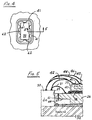
- Figure 4 is a fragmentary top plan view of another embodiment of a package for a semiconductor device according to the invention.
- Figure 5 is a fragmentary cross-sectional view taken along line 5-5 in Figure 4.
- the package includes a first generally planar body or layer of dielectric material 26 with metallization layers 27, 28 on the upper and lower surfaces thereof.
- This body has a generally rectangular central opening 29 in which a semiconductor die or chip 30 is mounted, with leads 31 extending between the die or chip and bonding pads formed in the metallization layer 27 on the upper side of the body.
- a heatsink 32 is bonded to the under side of body 26 in thermal contact with the chip and forms the floor of a cavity within the opening 29.
- the heatsink is fabricated of a thermally conductive material such as copper, tungsten, molybdenum, a ceramic, a tungsten-copper alloy, or a molybdenum-copper alloy, and it is bonded to body 26 by a suitable adhesive 33 such as epoxy or solder.
- a second body or layer of dielectric material 36 is mounted on the first body and has metallization layers 37, 38 on the upper and lower surfaces thereof.
- Body 36 has a generally rectangular central opening 39 of greater lateral extent than opening 29, and the metallization layer 38 on lower surface of this body wraps around the inner peripheral edge of the body, as indicated by the reference numeral 40, and extends along the inner margin of the upper surface of the body to form a conductive ring 41 to which leads 42 from the die or chip are bonded.
- Additional bonding pads and conductive traces 43 are formed in the metallization layer 37 outwardly of the conductive ring on the upper surface of body 36, and leads 44 from the die or chip are bonded to these pads and traces. Additional leads 46 from the die or chip are bonded to metallization layer 37 outwardly of pads 43.
- a third body or layer of dielectric material 47 is mounted on the second body, with metallization layers 48, 49 on the upper and lower surfaces thereof.
- Body 47 has a generally rectangular central opening 51 of greater lateral extent than opening 39, and a lid 52 is mounted on the upper side of this body to close the which the die or chip is mounted.
- Bodies 26, 36 and 47 are bonded together with layers 53, 54 of an electrically insulative adhesive.
- Bodies 26, 36 and the metallization layers 27, 37 on the upper surfaces thereof form bonding shelves or tiers to which the leads from die or chip 30 are attached, and the wraparound metallization 40 and conductive ring 41 provide means for making connections to the metallization layer 38 on the lower side of body 36.
- the supply voltage V CC is applied to layer 38, and connections to this voltage are made through the conductive ring.
- Other supply voltages and signals can be carried by other metallization layers as illustrated, and connections with these layers are made through bonding pads on the two shelves.
- Connections between the different layers in the package are made by vias such as those indicated by reference numerals 56-58.
- the metallization which wraps around the opening in the shelf can also wrap around additional layers of metallization, if desired.
- One or more such layers can be embedded in body 36, as indicated by dashed lines 59, and can be connected to or insulated electrically from the metallization which wraps around the shelf.
- FIG. 4-5 is generally similar to the embodiment of Figure 3, and like reference numerals designate corresponding elements in the two embodiments.
- the central opening 29 in body 26 is formed with a scalloped contour with fingers 61 which serve to locate or position the die, and relieved areas 62 between the fingers.
- the under sides of the fingers are cut away, as indicated at 63, to receive adhesive 64 which is squeezed out from between the die and the heatsink as the die is pressed into place, and the relieved areas permit cleaning and visual inspection of the adhesive 64 when the die is installed.
- Body 26 can be formed either as a single layer or body, with the under sides of the fingers being cut away by machining or another suitable process, or as two layers having the desired profiles for the fingers and the relieved areas beneath the fingers. It is also possible to cut the fingers to length after the artwork has been completed, using fiducials or landmarks on the artwork as guides to assure proper alignment of the die.
- the locating fingers are particularly helpful in the assembly of packages with staggered bonding pads where precise alignment of the die is important.
- the fingers hold the die in the proper position during curing of the adhesive which bonds the die to the heatsink and prevents the die from moving laterally as it is pressed toward the heatsink.
- the continuous wraparound shelf provides a continuous connection to a power source or termiating voltage and is more tolerant of die misalignment than the packages of the prior art.
Landscapes
- Wire Bonding (AREA)
- Cooling Or The Like Of Semiconductors Or Solid State Devices (AREA)
Applications Claiming Priority (2)
| Application Number | Priority Date | Filing Date | Title |
|---|---|---|---|
| US07/542,179 US5235211A (en) | 1990-06-22 | 1990-06-22 | Semiconductor package having wraparound metallization |
| US542179 | 1995-10-12 |
Publications (2)
| Publication Number | Publication Date |
|---|---|
| EP0463763A2 true EP0463763A2 (de) | 1992-01-02 |
| EP0463763A3 EP0463763A3 (en) | 1992-02-26 |
Family
ID=24162675
Family Applications (1)
| Application Number | Title | Priority Date | Filing Date |
|---|---|---|---|
| EP19910305223 Withdrawn EP0463763A3 (en) | 1990-06-22 | 1991-06-11 | Semiconductor package and method with wraparound metallization |
Country Status (4)
| Country | Link |
|---|---|
| US (1) | US5235211A (de) |
| EP (1) | EP0463763A3 (de) |
| JP (1) | JP2504636B2 (de) |
| KR (1) | KR950008238B1 (de) |
Cited By (8)
| Publication number | Priority date | Publication date | Assignee | Title |
|---|---|---|---|---|
| GB2293918A (en) * | 1994-10-06 | 1996-04-10 | Ibm | Electronic circuit packaging |
| WO1996025763A3 (en) * | 1995-02-15 | 1996-11-07 | Ibm | Organic chip carriers for wire bond-type chips |
| GB2317743A (en) * | 1996-06-07 | 1998-04-01 | Hewlett Packard Co | High density wirebond chip interconnect for multi-chip modules |
| EP0932328A4 (de) * | 1995-12-22 | 1999-10-27 | Ibiden Co Ltd | Substrat zur montierung eines elektronischen bauteils und verfahren zu dessen herstellung |
| EP1014436A3 (de) * | 1998-12-24 | 2001-07-11 | Shinko Electric Industries Co. Ltd. | Herstellung eines Substrates |
| US6441475B2 (en) * | 1999-09-13 | 2002-08-27 | Vishay Intertechnology, Inc. | Chip scale surface mount package for semiconductor device and process of fabricating the same |
| EP1480264A1 (de) * | 2003-05-21 | 2004-11-24 | Alps Electric Technology Centre (UK) Ltd. | Elektronisches Schaltkreis-Bauelement |
| EP1043921A4 (de) * | 1997-11-19 | 2007-02-21 | Ibiden Co Ltd | Mehrschichtige gedruckte leiterplatte und verfahren zu deren herstellung |
Families Citing this family (23)
| Publication number | Priority date | Publication date | Assignee | Title |
|---|---|---|---|---|
| JPH0810734B2 (ja) * | 1990-08-14 | 1996-01-31 | 松下電工株式会社 | 半導体チップキャリア |
| JPH06103721B2 (ja) * | 1990-09-25 | 1994-12-14 | 松下電工株式会社 | 半導体チップキャリア |
| JPH0595212A (ja) * | 1991-10-01 | 1993-04-16 | Mitsubishi Electric Corp | 高周波半導体混成集積回路装置 |
| US5777265A (en) * | 1993-01-21 | 1998-07-07 | Intel Corporation | Multilayer molded plastic package design |
| US5397917A (en) * | 1993-04-26 | 1995-03-14 | Motorola, Inc. | Semiconductor package capable of spreading heat |
| US5701034A (en) * | 1994-05-03 | 1997-12-23 | Amkor Electronics, Inc. | Packaged semiconductor die including heat sink with locking feature |
| US5530287A (en) * | 1994-09-14 | 1996-06-25 | Unisys Corporation | High density wire bond pattern for integratd circuit package |
| US5625227A (en) * | 1995-01-18 | 1997-04-29 | Dell Usa, L.P. | Circuit board-mounted IC package cooling apparatus |
| US5705174A (en) * | 1995-06-07 | 1998-01-06 | American Cyanamid Company | Process for the preparation of microcapsule compositions |
| US6031283A (en) * | 1996-09-09 | 2000-02-29 | Intel Corporation | Integrated circuit package |
| US6043559A (en) * | 1996-09-09 | 2000-03-28 | Intel Corporation | Integrated circuit package which contains two in plane voltage busses and a wrap around conductive strip that connects a bond finger to one of the busses |
| US6081426A (en) * | 1996-09-18 | 2000-06-27 | Shinko Electric Industries Co., Ltd. | Semiconductor package having a heat slug |
| KR19980024134A (ko) * | 1996-09-18 | 1998-07-06 | 모기 쥰이찌 | 반도체 패키지 |
| US6794581B2 (en) * | 2000-10-30 | 2004-09-21 | Sun Microsystems, Inc. | Method and apparatus for distributing power to integrated circuits |
| US20040183167A1 (en) * | 2003-03-21 | 2004-09-23 | Texas Instruments Incorporated | Recessed-bond semiconductor package substrate |
| US7019394B2 (en) * | 2003-09-30 | 2006-03-28 | Intel Corporation | Circuit package and method of plating the same |
| US20070000686A1 (en) * | 2005-06-29 | 2007-01-04 | Martinez Peter J | System, method and apparatus for routing signals from an integrated circuit using thickfilm and printed circuit interconnects |
| US9713258B2 (en) * | 2006-04-27 | 2017-07-18 | International Business Machines Corporation | Integrated circuit chip packaging |
| US20090283889A1 (en) * | 2008-05-16 | 2009-11-19 | Byoung Wook Jang | Integrated circuit package system |
| US8354743B2 (en) * | 2010-01-27 | 2013-01-15 | Honeywell International Inc. | Multi-tiered integrated circuit package |
| US10347559B2 (en) | 2011-03-16 | 2019-07-09 | Momentive Performance Materials Inc. | High thermal conductivity/low coefficient of thermal expansion composites |
| US9741644B2 (en) | 2015-05-04 | 2017-08-22 | Honeywell International Inc. | Stacking arrangement for integration of multiple integrated circuits |
| US20220230944A1 (en) * | 2020-12-31 | 2022-07-21 | Texas Instruments Incorporated | Configurable leaded package |
Family Cites Families (10)
| Publication number | Priority date | Publication date | Assignee | Title |
|---|---|---|---|---|
| US3908185A (en) * | 1974-03-06 | 1975-09-23 | Rca Corp | High frequency semiconductor device having improved metallized patterns |
| US4420767A (en) * | 1978-11-09 | 1983-12-13 | Zilog, Inc. | Thermally balanced leadless microelectronic circuit chip carrier |
| JPS5875859A (ja) * | 1981-10-30 | 1983-05-07 | Fujitsu Ltd | 半導体装置 |
| US4608592A (en) * | 1982-07-09 | 1986-08-26 | Nec Corporation | Semiconductor device provided with a package for a semiconductor element having a plurality of electrodes to be applied with substantially same voltage |
| JPS5914652A (ja) * | 1982-07-16 | 1984-01-25 | Nec Corp | 半導体容器 |
| JPS60116191A (ja) * | 1983-11-29 | 1985-06-22 | イビデン株式会社 | 電子部品搭載用基板の製造方法 |
| US4922324A (en) * | 1987-01-20 | 1990-05-01 | Kabushiki Kaisha Toshiba | Semiconductor integrated circuit device |
| JPS63250845A (ja) * | 1987-04-08 | 1988-10-18 | Hitachi Ltd | 半導体パツケ−ジ構造体 |
| JPS6484698A (en) * | 1987-09-26 | 1989-03-29 | Matsushita Electric Works Ltd | Manufacture of multilayer circuit board |
| US4926240A (en) * | 1989-03-28 | 1990-05-15 | Motorola, Inc. | Semiconductor package having recessed die cavity walls |
-
1990
- 1990-06-22 US US07/542,179 patent/US5235211A/en not_active Expired - Lifetime
-
1991
- 1991-06-11 EP EP19910305223 patent/EP0463763A3/en not_active Withdrawn
- 1991-06-21 JP JP3150065A patent/JP2504636B2/ja not_active Expired - Lifetime
- 1991-06-22 KR KR1019910010460A patent/KR950008238B1/ko not_active Expired - Fee Related
Cited By (9)
| Publication number | Priority date | Publication date | Assignee | Title |
|---|---|---|---|---|
| GB2293918A (en) * | 1994-10-06 | 1996-04-10 | Ibm | Electronic circuit packaging |
| WO1996025763A3 (en) * | 1995-02-15 | 1996-11-07 | Ibm | Organic chip carriers for wire bond-type chips |
| EP0932328A4 (de) * | 1995-12-22 | 1999-10-27 | Ibiden Co Ltd | Substrat zur montierung eines elektronischen bauteils und verfahren zu dessen herstellung |
| US6201185B1 (en) | 1995-12-22 | 2001-03-13 | Ibiden Co., Ltd. | Substrate for mounting electronic part having conductive projections and process for manufacturing the same |
| GB2317743A (en) * | 1996-06-07 | 1998-04-01 | Hewlett Packard Co | High density wirebond chip interconnect for multi-chip modules |
| EP1043921A4 (de) * | 1997-11-19 | 2007-02-21 | Ibiden Co Ltd | Mehrschichtige gedruckte leiterplatte und verfahren zu deren herstellung |
| EP1014436A3 (de) * | 1998-12-24 | 2001-07-11 | Shinko Electric Industries Co. Ltd. | Herstellung eines Substrates |
| US6441475B2 (en) * | 1999-09-13 | 2002-08-27 | Vishay Intertechnology, Inc. | Chip scale surface mount package for semiconductor device and process of fabricating the same |
| EP1480264A1 (de) * | 2003-05-21 | 2004-11-24 | Alps Electric Technology Centre (UK) Ltd. | Elektronisches Schaltkreis-Bauelement |
Also Published As
| Publication number | Publication date |
|---|---|
| JPH04250641A (ja) | 1992-09-07 |
| KR950008238B1 (ko) | 1995-07-26 |
| KR920001693A (ko) | 1992-01-30 |
| US5235211A (en) | 1993-08-10 |
| EP0463763A3 (en) | 1992-02-26 |
| JP2504636B2 (ja) | 1996-06-05 |
Similar Documents
| Publication | Publication Date | Title |
|---|---|---|
| US5235211A (en) | Semiconductor package having wraparound metallization | |
| US5552631A (en) | Semiconductor device assembly including power or ground plane which is provided on opposite surface of insulating layer from signal traces, and is exposed to central opening in insulating layer for interconnection to semiconductor die | |
| US6448659B1 (en) | Stacked die design with supporting O-ring | |
| US5477082A (en) | Bi-planar multi-chip module | |
| KR100372153B1 (ko) | 다층리드프레임 | |
| US5376588A (en) | Method for making high pin count package for semiconductor device | |
| US7307353B2 (en) | Technique for attaching die to leads | |
| EP0247775B1 (de) | Halbleiterpackung mit Eingang/Ausgang-Verbindungen hoher Dichte | |
| KR100328143B1 (ko) | 계층화된 도전 평면을 갖는 리드 프레임 | |
| EP0645811B1 (de) | Halbleiteranordnung mit einem Halbleiterchip mit Rückseitenelektrode | |
| EP0380906A2 (de) | Halbleiteranordnung vom Bandmontage-Typ | |
| US5751554A (en) | Testable chip carrier | |
| US5309322A (en) | Leadframe strip for semiconductor packages and method | |
| JPH09507344A (ja) | ワイヤ・ボンディングの技術に基づくボール・グリッド・アレイの下に浅い空洞を持つパッケージ | |
| JPH08195329A (ja) | 集積回路における薄膜チップコンデンサ及びその製造方法 | |
| JPH03779B2 (de) | ||
| KR100255476B1 (ko) | 볼 그리드 어레이 패키지 | |
| US6337226B1 (en) | Semiconductor package with supported overhanging upper die | |
| US6380634B1 (en) | Conductor wires and semiconductor device using them | |
| US5854085A (en) | Multi-layer tab tape having distinct signal, power and ground planes, semiconductor device assembly employing same, apparatus for and method of assembling same | |
| CN215118900U (zh) | 半导体器件封装件 | |
| WO1994025983A1 (en) | Semiconductor chip packaging method and semiconductor chip having interdigitated gate runners with gate bonding pads | |
| US6111311A (en) | Semiconductor device and method of forming the same | |
| US4831495A (en) | Unitized packaging arrangement for an energy dissipating device | |
| JP3269025B2 (ja) | 半導体装置とその製造方法 |
Legal Events
| Date | Code | Title | Description |
|---|---|---|---|
| PUAI | Public reference made under article 153(3) epc to a published international application that has entered the european phase |
Free format text: ORIGINAL CODE: 0009012 |
|
| 17P | Request for examination filed |
Effective date: 19910626 |
|
| AK | Designated contracting states |
Kind code of ref document: A2 Designated state(s): DE FR GB IT |
|
| PUAL | Search report despatched |
Free format text: ORIGINAL CODE: 0009013 |
|
| AK | Designated contracting states |
Kind code of ref document: A3 Designated state(s): DE FR GB IT |
|
| 17Q | First examination report despatched |
Effective date: 19940720 |
|
| APAB | Appeal dossier modified |
Free format text: ORIGINAL CODE: EPIDOS NOAPE |
|
| APAB | Appeal dossier modified |
Free format text: ORIGINAL CODE: EPIDOS NOAPE |
|
| APAD | Appeal reference recorded |
Free format text: ORIGINAL CODE: EPIDOS REFNE |
|
| APAD | Appeal reference recorded |
Free format text: ORIGINAL CODE: EPIDOS REFNE |
|
| APAB | Appeal dossier modified |
Free format text: ORIGINAL CODE: EPIDOS NOAPE |
|
| STAA | Information on the status of an ep patent application or granted ep patent |
Free format text: STATUS: THE APPLICATION IS DEEMED TO BE WITHDRAWN |
|
| 18D | Application deemed to be withdrawn |
Effective date: 19991231 |
|
| APAF | Appeal reference modified |
Free format text: ORIGINAL CODE: EPIDOSCREFNE |