EP0464372A2 - Procédé pour fabriquer et passiver des dispositifs semi-conducteurs - Google Patents
Procédé pour fabriquer et passiver des dispositifs semi-conducteurs Download PDFInfo
- Publication number
- EP0464372A2 EP0464372A2 EP19910108781 EP91108781A EP0464372A2 EP 0464372 A2 EP0464372 A2 EP 0464372A2 EP 19910108781 EP19910108781 EP 19910108781 EP 91108781 A EP91108781 A EP 91108781A EP 0464372 A2 EP0464372 A2 EP 0464372A2
- Authority
- EP
- European Patent Office
- Prior art keywords
- layer
- plasma
- halogen
- substrate
- passivation layer
- Prior art date
- Legal status (The legal status is an assumption and is not a legal conclusion. Google has not performed a legal analysis and makes no representation as to the accuracy of the status listed.)
- Granted
Links
Images


Classifications
-
- H—ELECTRICITY
- H10—SEMICONDUCTOR DEVICES; ELECTRIC SOLID-STATE DEVICES NOT OTHERWISE PROVIDED FOR
- H10P—GENERIC PROCESSES OR APPARATUS FOR THE MANUFACTURE OR TREATMENT OF DEVICES COVERED BY CLASS H10
- H10P14/00—Formation of materials, e.g. in the shape of layers or pillars
- H10P14/60—Formation of materials, e.g. in the shape of layers or pillars of insulating materials
- H10P14/65—Formation of materials, e.g. in the shape of layers or pillars of insulating materials characterised by treatments performed before or after the formation of the materials
- H10P14/6502—Formation of materials, e.g. in the shape of layers or pillars of insulating materials characterised by treatments performed before or after the formation of the materials of treatments performed before formation of the materials
- H10P14/6512—Formation of materials, e.g. in the shape of layers or pillars of insulating materials characterised by treatments performed before or after the formation of the materials of treatments performed before formation of the materials by exposure to a gas or vapour
- H10P14/6514—Formation of materials, e.g. in the shape of layers or pillars of insulating materials characterised by treatments performed before or after the formation of the materials of treatments performed before formation of the materials by exposure to a gas or vapour by exposure to a plasma
-
- H—ELECTRICITY
- H10—SEMICONDUCTOR DEVICES; ELECTRIC SOLID-STATE DEVICES NOT OTHERWISE PROVIDED FOR
- H10F—INORGANIC SEMICONDUCTOR DEVICES SENSITIVE TO INFRARED RADIATION, LIGHT, ELECTROMAGNETIC RADIATION OF SHORTER WAVELENGTH OR CORPUSCULAR RADIATION
- H10F71/00—Manufacture or treatment of devices covered by this subclass
- H10F71/127—The active layers comprising only Group III-V materials, e.g. GaAs or InP
-
- H—ELECTRICITY
- H10—SEMICONDUCTOR DEVICES; ELECTRIC SOLID-STATE DEVICES NOT OTHERWISE PROVIDED FOR
- H10F—INORGANIC SEMICONDUCTOR DEVICES SENSITIVE TO INFRARED RADIATION, LIGHT, ELECTROMAGNETIC RADIATION OF SHORTER WAVELENGTH OR CORPUSCULAR RADIATION
- H10F77/00—Constructional details of devices covered by this subclass
- H10F77/30—Coatings
- H10F77/306—Coatings for devices having potential barriers
-
- H—ELECTRICITY
- H10—SEMICONDUCTOR DEVICES; ELECTRIC SOLID-STATE DEVICES NOT OTHERWISE PROVIDED FOR
- H10P—GENERIC PROCESSES OR APPARATUS FOR THE MANUFACTURE OR TREATMENT OF DEVICES COVERED BY CLASS H10
- H10P14/00—Formation of materials, e.g. in the shape of layers or pillars
- H10P14/60—Formation of materials, e.g. in the shape of layers or pillars of insulating materials
- H10P14/63—Formation of materials, e.g. in the shape of layers or pillars of insulating materials characterised by the formation processes
- H10P14/6326—Deposition processes
- H10P14/6328—Deposition from the gas or vapour phase
- H10P14/6334—Deposition from the gas or vapour phase using decomposition or reaction of gaseous or vapour phase compounds, i.e. chemical vapour deposition
- H10P14/6336—Deposition from the gas or vapour phase using decomposition or reaction of gaseous or vapour phase compounds, i.e. chemical vapour deposition in the presence of a plasma [PECVD]
-
- H—ELECTRICITY
- H10—SEMICONDUCTOR DEVICES; ELECTRIC SOLID-STATE DEVICES NOT OTHERWISE PROVIDED FOR
- H10P—GENERIC PROCESSES OR APPARATUS FOR THE MANUFACTURE OR TREATMENT OF DEVICES COVERED BY CLASS H10
- H10P14/00—Formation of materials, e.g. in the shape of layers or pillars
- H10P14/60—Formation of materials, e.g. in the shape of layers or pillars of insulating materials
- H10P14/69—Inorganic materials
- H10P14/692—Inorganic materials composed of oxides, glassy oxides or oxide-based glasses
- H10P14/6921—Inorganic materials composed of oxides, glassy oxides or oxide-based glasses containing silicon
- H10P14/69215—Inorganic materials composed of oxides, glassy oxides or oxide-based glasses containing silicon the material being a silicon oxide, e.g. SiO2
-
- H—ELECTRICITY
- H10—SEMICONDUCTOR DEVICES; ELECTRIC SOLID-STATE DEVICES NOT OTHERWISE PROVIDED FOR
- H10P—GENERIC PROCESSES OR APPARATUS FOR THE MANUFACTURE OR TREATMENT OF DEVICES COVERED BY CLASS H10
- H10P14/00—Formation of materials, e.g. in the shape of layers or pillars
- H10P14/60—Formation of materials, e.g. in the shape of layers or pillars of insulating materials
- H10P14/69—Inorganic materials
- H10P14/692—Inorganic materials composed of oxides, glassy oxides or oxide-based glasses
- H10P14/6921—Inorganic materials composed of oxides, glassy oxides or oxide-based glasses containing silicon
- H10P14/6922—Inorganic materials composed of oxides, glassy oxides or oxide-based glasses containing silicon the material containing Si, O and at least one of H, N, C, F or other non-metal elements, e.g. SiOC, SiOC:H or SiONC
- H10P14/6927—Inorganic materials composed of oxides, glassy oxides or oxide-based glasses containing silicon the material containing Si, O and at least one of H, N, C, F or other non-metal elements, e.g. SiOC, SiOC:H or SiONC the material being a silicon oxynitride, e.g. SiON or SiON:H
-
- H—ELECTRICITY
- H10—SEMICONDUCTOR DEVICES; ELECTRIC SOLID-STATE DEVICES NOT OTHERWISE PROVIDED FOR
- H10P—GENERIC PROCESSES OR APPARATUS FOR THE MANUFACTURE OR TREATMENT OF DEVICES COVERED BY CLASS H10
- H10P14/00—Formation of materials, e.g. in the shape of layers or pillars
- H10P14/60—Formation of materials, e.g. in the shape of layers or pillars of insulating materials
- H10P14/69—Inorganic materials
- H10P14/694—Inorganic materials composed of nitrides
- H10P14/6943—Inorganic materials composed of nitrides containing silicon
- H10P14/69433—Inorganic materials composed of nitrides containing silicon the material being a silicon nitride not containing oxygen, e.g. SixNy or SixByNz
-
- H—ELECTRICITY
- H10—SEMICONDUCTOR DEVICES; ELECTRIC SOLID-STATE DEVICES NOT OTHERWISE PROVIDED FOR
- H10P—GENERIC PROCESSES OR APPARATUS FOR THE MANUFACTURE OR TREATMENT OF DEVICES COVERED BY CLASS H10
- H10P70/00—Cleaning of wafers, substrates or parts of devices
- H10P70/10—Cleaning before device manufacture, i.e. Begin-Of-Line process
- H10P70/12—Cleaning before device manufacture, i.e. Begin-Of-Line process by dry cleaning only
-
- Y—GENERAL TAGGING OF NEW TECHNOLOGICAL DEVELOPMENTS; GENERAL TAGGING OF CROSS-SECTIONAL TECHNOLOGIES SPANNING OVER SEVERAL SECTIONS OF THE IPC; TECHNICAL SUBJECTS COVERED BY FORMER USPC CROSS-REFERENCE ART COLLECTIONS [XRACs] AND DIGESTS
- Y02—TECHNOLOGIES OR APPLICATIONS FOR MITIGATION OR ADAPTATION AGAINST CLIMATE CHANGE
- Y02E—REDUCTION OF GREENHOUSE GAS [GHG] EMISSIONS, RELATED TO ENERGY GENERATION, TRANSMISSION OR DISTRIBUTION
- Y02E10/00—Energy generation through renewable energy sources
- Y02E10/50—Photovoltaic [PV] energy
- Y02E10/544—Solar cells from Group III-V materials
-
- Y—GENERAL TAGGING OF NEW TECHNOLOGICAL DEVELOPMENTS; GENERAL TAGGING OF CROSS-SECTIONAL TECHNOLOGIES SPANNING OVER SEVERAL SECTIONS OF THE IPC; TECHNICAL SUBJECTS COVERED BY FORMER USPC CROSS-REFERENCE ART COLLECTIONS [XRACs] AND DIGESTS
- Y02—TECHNOLOGIES OR APPLICATIONS FOR MITIGATION OR ADAPTATION AGAINST CLIMATE CHANGE
- Y02P—CLIMATE CHANGE MITIGATION TECHNOLOGIES IN THE PRODUCTION OR PROCESSING OF GOODS
- Y02P70/00—Climate change mitigation technologies in the production process for final industrial or consumer products
- Y02P70/50—Manufacturing or production processes characterised by the final manufactured product
-
- Y—GENERAL TAGGING OF NEW TECHNOLOGICAL DEVELOPMENTS; GENERAL TAGGING OF CROSS-SECTIONAL TECHNOLOGIES SPANNING OVER SEVERAL SECTIONS OF THE IPC; TECHNICAL SUBJECTS COVERED BY FORMER USPC CROSS-REFERENCE ART COLLECTIONS [XRACs] AND DIGESTS
- Y10—TECHNICAL SUBJECTS COVERED BY FORMER USPC
- Y10S—TECHNICAL SUBJECTS COVERED BY FORMER USPC CROSS-REFERENCE ART COLLECTIONS [XRACs] AND DIGESTS
- Y10S438/00—Semiconductor device manufacturing: process
- Y10S438/958—Passivation layer
Definitions
- the invention relates to a method according to the preamble of patent claim 1.
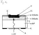
- Fig. 1 shows a known planar InGaAs / InP-pin photodiode in different phases of its formation.
- FIG. 1a shows a two-layer substrate S made of n-doped indium phosphide InP and also n-doped indium gallium arsenide (InGaAs) applied thereon. Since, for example, Zn or Cd is to be diffused into this substrate S to form a p-conducting region, it is covered with an insulating layer IS made of SiO x , SiN y or SiO x N y to delimit this region, which is photolithographically predetermined with an opening L. Form and surface was provided. The insulating layer thus represents a diffusion mask.
- 1b shows the substrate S with the p-doped region P produced by diffusion and the electrically active pn junction located at its boundary with the n-doped substrate.
- FIG. 1c finally, shows the finished pin photodiode with applied metallic contacts K, an antireflection layer A on a light entry surface and with a passivation layer PS which, after removing the diffusion mask, the n-doped and the p-doped region on the top of the substrate covered.
- the component shown in FIGS. 1a to 1c in different stages of construction can be manufactured in different ways.
- the structure of the individual semiconductor and insulator layers can e.g. by sputtering or by separating a chemical reaction product from the vapor phase (Chemical Vapor Deposition CVD).
- the latter method has become known as thermal CVD, plasma-assisted CVD (also PECVD) or photo-CVD, depending on whether heat, a plasma or short-wave light are used to stimulate the chemical reaction.
- the component shown in FIGS. 1a to 1c and manufactured in a conventional manner has inadequate electrical properties, in particular an excessively high reverse current (dark current).
- Various investigations which will not be dealt with in more detail here, found damage to the semiconductor surface in the region of the pn junction (region B in FIG. 1c) as the cause of this inadequacy, which apparently contributes to the action of an intrinsic oxide layer present on the semiconductor surface the application of diffusion masking or passivation layers.
- a plasma-assisted CVD process differs from conventional processes of this type in that a pre-treatment of the surface to be coated is carried out in a halogen-carbon plasma before applying an insulating layer or a passivation layer which serves for diffusion masking.
- a pre-treatment of the surface to be coated is carried out in a halogen-carbon plasma before applying an insulating layer or a passivation layer which serves for diffusion masking.
- the substrate surface to be coated is introduced into a commercially available PECVD parallel plate reactor and heated to a temperature of approximately 200 ° C.
- a CF4 atmosphere with a pressure of 0.8 mbar is then produced in the reactor via inlet and outlet ports and a plasma is generated by applying an HF voltage to the electrode plates of the reactor.
- the CF4 is replaced by other reaction gases (for example SiH4, N20, N2) required to build up the insulating or passivating layer and the substrate is coated for about 6 to 7 minutes.
- the resulting layer can consist of Si02, Si3N4 or Si0 x N y depending on the composition of the reaction gases.
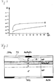
- the electrical values of a photodiode produced by this method are extremely improved compared to those of such components produced by known methods.
- 2 shows, for example, dark current characteristics, one each on InGaAs (II) and one on InP (I), according to the method described above, planar pin photodiode.
- the described method is suitable for avoiding damage to the semiconductor surface when applying insulating or passivating layers, both for InGaAs and InP substrates, and thus to enable the production of components with good and stable electrical values .
- the described method is not restricted to pin photodiodes and not to planar components.
- 3 shows, for example, the structure of a planar double hetero-APD, in which the passivation layer IS made of SiN x can be applied after pretreatment of the substrate surface in accordance with the described method.
- FIG 4 shows a MESA pin diode with a passivation layer PS applied by the described method.
Landscapes
- Formation Of Insulating Films (AREA)
- Light Receiving Elements (AREA)
- Crystals, And After-Treatments Of Crystals (AREA)
- Mechanical Treatment Of Semiconductor (AREA)
Applications Claiming Priority (2)
| Application Number | Priority Date | Filing Date | Title |
|---|---|---|---|
| DE4017870 | 1990-06-02 | ||
| DE4017870A DE4017870A1 (de) | 1990-06-02 | 1990-06-02 | Verfahren zur herstellung und passivierung von halbleiterbauelementen |
Publications (3)
| Publication Number | Publication Date |
|---|---|
| EP0464372A2 true EP0464372A2 (fr) | 1992-01-08 |
| EP0464372A3 EP0464372A3 (en) | 1992-05-27 |
| EP0464372B1 EP0464372B1 (fr) | 1997-04-23 |
Family
ID=6407742
Family Applications (1)
| Application Number | Title | Priority Date | Filing Date |
|---|---|---|---|
| EP91108781A Expired - Lifetime EP0464372B1 (fr) | 1990-06-02 | 1991-05-29 | Procédé pour fabriquer et passiver des dispositifs semi-conducteurs |
Country Status (6)
| Country | Link |
|---|---|
| US (1) | US5248635A (fr) |
| EP (1) | EP0464372B1 (fr) |
| JP (1) | JP3207869B2 (fr) |
| AT (1) | ATE152289T1 (fr) |
| DE (2) | DE4017870A1 (fr) |
| ES (1) | ES2103285T3 (fr) |
Cited By (1)
| Publication number | Priority date | Publication date | Assignee | Title |
|---|---|---|---|---|
| US20210351037A1 (en) * | 2018-10-05 | 2021-11-11 | Osram Opto Semiconductors Gmbh | Method for producing a semiconductor component comprising performing a plasma treatment, and semiconductor component |
Families Citing this family (6)
| Publication number | Priority date | Publication date | Assignee | Title |
|---|---|---|---|---|
| US5593902A (en) * | 1994-05-23 | 1997-01-14 | Texas Instruments Incorporated | Method of making photodiodes for low dark current operation having geometric enhancement |
| US5888890A (en) * | 1994-08-12 | 1999-03-30 | Lg Semicon Co., Ltd. | Method of manufacturing field effect transistor |
| US20040241948A1 (en) * | 2003-05-29 | 2004-12-02 | Chun-Feng Nieh | Method of fabricating stacked gate dielectric layer |
| DE10359371A1 (de) * | 2003-12-18 | 2005-07-28 | Fraunhofer-Gesellschaft zur Förderung der angewandten Forschung e.V. | Passivierte Endoberflächen |
| US10020187B2 (en) | 2012-11-26 | 2018-07-10 | Applied Materials, Inc. | Apparatus and methods for backside passivation |
| US10666353B1 (en) * | 2018-11-20 | 2020-05-26 | Juniper Networks, Inc. | Normal incidence photodetector with self-test functionality |
Family Cites Families (6)
| Publication number | Priority date | Publication date | Assignee | Title |
|---|---|---|---|---|
| US3969164A (en) * | 1974-09-16 | 1976-07-13 | Bell Telephone Laboratories, Incorporated | Native oxide technique for preparing clean substrate surfaces |
| US4246296A (en) * | 1979-02-14 | 1981-01-20 | Bell Telephone Laboratories, Incorporated | Controlling the properties of native films using selective growth chemistry |
| US4455351A (en) * | 1983-06-13 | 1984-06-19 | At&T Bell Laboratories | Preparation of photodiodes |
| US4987008A (en) * | 1985-07-02 | 1991-01-22 | Semiconductor Energy Laboratory Co., Ltd. | Thin film formation method |
| US4830705A (en) * | 1987-07-16 | 1989-05-16 | Texas Instruments Incorporated | Method for etch of GaAs |
| US5098851A (en) * | 1989-02-10 | 1992-03-24 | Hitachi, Ltd. | Fabricating a semiconductor photodetector by annealing to smooth the PN junction |
-
1990
- 1990-06-02 DE DE4017870A patent/DE4017870A1/de not_active Withdrawn
-
1991
- 1991-05-28 JP JP15247991A patent/JP3207869B2/ja not_active Expired - Fee Related
- 1991-05-29 EP EP91108781A patent/EP0464372B1/fr not_active Expired - Lifetime
- 1991-05-29 US US07/707,047 patent/US5248635A/en not_active Expired - Fee Related
- 1991-05-29 DE DE59108673T patent/DE59108673D1/de not_active Expired - Fee Related
- 1991-05-29 AT AT91108781T patent/ATE152289T1/de not_active IP Right Cessation
- 1991-05-29 ES ES91108781T patent/ES2103285T3/es not_active Expired - Lifetime
Cited By (2)
| Publication number | Priority date | Publication date | Assignee | Title |
|---|---|---|---|---|
| US20210351037A1 (en) * | 2018-10-05 | 2021-11-11 | Osram Opto Semiconductors Gmbh | Method for producing a semiconductor component comprising performing a plasma treatment, and semiconductor component |
| US11915935B2 (en) * | 2018-10-05 | 2024-02-27 | Osram Opto Semiconductors Gmbh | Method for producing a semiconductor component comprising performing a plasma treatment, and semiconductor component |
Also Published As
| Publication number | Publication date |
|---|---|
| US5248635A (en) | 1993-09-28 |
| DE4017870A1 (de) | 1991-12-05 |
| EP0464372A3 (en) | 1992-05-27 |
| DE59108673D1 (de) | 1997-05-28 |
| JPH04230033A (ja) | 1992-08-19 |
| ES2103285T3 (es) | 1997-09-16 |
| EP0464372B1 (fr) | 1997-04-23 |
| JP3207869B2 (ja) | 2001-09-10 |
| ATE152289T1 (de) | 1997-05-15 |
Similar Documents
| Publication | Publication Date | Title |
|---|---|---|
| EP0813753B1 (fr) | Cellule solaire avec champ electrique arriere et procede de fabrication de ladite cellule | |
| EP0607180B1 (fr) | Procede de fabrication de composants semi-conducteurs | |
| DE3650287T2 (de) | Halbleiter-Photodetektor mit einem zweistufigen Verunreinigungsprofil. | |
| DE19634617B4 (de) | Verfahren zur Herstellung einer Siliziumsolarzelle mit verringerter Rekombination nahe der Solarzellenoberfläche | |
| DE69421014T2 (de) | Widerstandsbestimmungsmethode von N-Typ-Siliziumepitaxieschichten | |
| DE3511675A1 (de) | Antireflexfilm fuer eine photoelektrische einrichtung und herstellungsverfahren dazu | |
| EP1068646A1 (fr) | Procede permettant de doper d'un seul cote un dispositif a semi-conducteur | |
| DE3700620A1 (de) | Halbleiterkoerper und verfahren zum herstellen desselben | |
| DE2920444C2 (de) | Verfahren zur ohmschen Kontaktierung eines Halbleiterbauelements | |
| EP2338179B1 (fr) | Procédé de traitement de substrats et dispositif de traitement pour mettre en oeuvre le procédé | |
| DE69623000T2 (de) | Elektrolumineszentes Bauelement, das poröses Silicium enthält | |
| EP0464372B1 (fr) | Procédé pour fabriquer et passiver des dispositifs semi-conducteurs | |
| DE3340874A1 (de) | Verfahren zum herstellen einer solarzelle | |
| DE2735937C2 (de) | Flüssigphasenepitaxie-Verfahren zur Herstellung von Halbleiter-Heterostrukturen | |
| DE2554029C2 (de) | Verfahren zur Erzeugung optoelektronischer Anordnungen | |
| DE102014205350B4 (de) | Photoaktives Halbleiterbauelement sowie Verfahren zum Herstellen eines photoaktiven Halbleiterbauelementes | |
| DE3015422A1 (de) | Verfahren zur herstellung einer elektrolumineszierenden halbleiteranordnung und durch dieses verfahren hergestellte elektrolumineszierende halbleiteranordnung | |
| DE19920871B4 (de) | Verfahren zum Aktivieren von Ladungsträgern durch strahlungsunterstützte Wärmebehandlung | |
| DE2734726C2 (de) | Verfahren zum Herstellen einer Silicium-Lawinen-Photodioden | |
| DE2755168A1 (de) | Verfahren zur herstellung von halbleiterbauelementen | |
| DE69001016T2 (de) | Verfahren zur herstellung von wolfram-antimon ohmischen kontakten mit niedrigem widerstand auf iii-iv halbleitermaterialien. | |
| DE102008044882A1 (de) | Verfahren zur lokalen Kontaktierung und lokalen Dotierung einer Halbleiterschicht | |
| DE1816082A1 (de) | Verfahren zum Herstellen von diffundierten Halbleiterbauelementen aus Silicium | |
| EP0706207B1 (fr) | Procédé pour reduire la vitesse de recombinaison en surface du silicium | |
| DE2048201A1 (de) | Halbleitervorrichtung |
Legal Events
| Date | Code | Title | Description |
|---|---|---|---|
| PUAI | Public reference made under article 153(3) epc to a published international application that has entered the european phase |
Free format text: ORIGINAL CODE: 0009012 |
|
| AK | Designated contracting states |
Kind code of ref document: A2 Designated state(s): AT BE CH DE ES FR GB IT LI NL SE |
|
| PUAL | Search report despatched |
Free format text: ORIGINAL CODE: 0009013 |
|
| AK | Designated contracting states |
Kind code of ref document: A3 Designated state(s): AT BE CH DE ES FR GB IT LI NL SE |
|
| 17P | Request for examination filed |
Effective date: 19920626 |
|
| RAP3 | Party data changed (applicant data changed or rights of an application transferred) |
Owner name: ALCATEL N.V. Owner name: ALCATEL SEL AKTIENGESELLSCHAFT |
|
| 17Q | First examination report despatched |
Effective date: 19941004 |
|
| GRAG | Despatch of communication of intention to grant |
Free format text: ORIGINAL CODE: EPIDOS AGRA |
|
| GRAH | Despatch of communication of intention to grant a patent |
Free format text: ORIGINAL CODE: EPIDOS IGRA |
|
| GRAH | Despatch of communication of intention to grant a patent |
Free format text: ORIGINAL CODE: EPIDOS IGRA |
|
| GRAA | (expected) grant |
Free format text: ORIGINAL CODE: 0009210 |
|
| AK | Designated contracting states |
Kind code of ref document: B1 Designated state(s): AT BE CH DE ES FR GB IT LI NL SE |
|
| REF | Corresponds to: |
Ref document number: 152289 Country of ref document: AT Date of ref document: 19970515 Kind code of ref document: T |
|
| REG | Reference to a national code |
Ref country code: CH Ref legal event code: NV Representative=s name: JUERG ULRICH C/O ALCATEL STR AG Ref country code: CH Ref legal event code: EP |
|
| REF | Corresponds to: |
Ref document number: 59108673 Country of ref document: DE Date of ref document: 19970528 |
|
| ITF | It: translation for a ep patent filed | ||
| GBT | Gb: translation of ep patent filed (gb section 77(6)(a)/1977) |
Effective date: 19970508 |
|
| ET | Fr: translation filed | ||
| REG | Reference to a national code |
Ref country code: ES Ref legal event code: FG2A Ref document number: 2103285 Country of ref document: ES Kind code of ref document: T3 |
|
| PLBE | No opposition filed within time limit |
Free format text: ORIGINAL CODE: 0009261 |
|
| STAA | Information on the status of an ep patent application or granted ep patent |
Free format text: STATUS: NO OPPOSITION FILED WITHIN TIME LIMIT |
|
| 26N | No opposition filed | ||
| PGFP | Annual fee paid to national office [announced via postgrant information from national office to epo] |
Ref country code: CH Payment date: 20010418 Year of fee payment: 11 |
|
| PGFP | Annual fee paid to national office [announced via postgrant information from national office to epo] |
Ref country code: AT Payment date: 20010427 Year of fee payment: 11 |
|
| PGFP | Annual fee paid to national office [announced via postgrant information from national office to epo] |
Ref country code: ES Payment date: 20010514 Year of fee payment: 11 Ref country code: BE Payment date: 20010514 Year of fee payment: 11 |
|
| REG | Reference to a national code |
Ref country code: GB Ref legal event code: IF02 |
|
| PGFP | Annual fee paid to national office [announced via postgrant information from national office to epo] |
Ref country code: NL Payment date: 20020430 Year of fee payment: 12 |
|
| PGFP | Annual fee paid to national office [announced via postgrant information from national office to epo] |
Ref country code: SE Payment date: 20020502 Year of fee payment: 12 Ref country code: GB Payment date: 20020502 Year of fee payment: 12 |
|
| PGFP | Annual fee paid to national office [announced via postgrant information from national office to epo] |
Ref country code: DE Payment date: 20020511 Year of fee payment: 12 |
|
| PGFP | Annual fee paid to national office [announced via postgrant information from national office to epo] |
Ref country code: FR Payment date: 20020513 Year of fee payment: 12 |
|
| PG25 | Lapsed in a contracting state [announced via postgrant information from national office to epo] |
Ref country code: AT Free format text: LAPSE BECAUSE OF NON-PAYMENT OF DUE FEES Effective date: 20020529 |
|
| PG25 | Lapsed in a contracting state [announced via postgrant information from national office to epo] |
Ref country code: ES Free format text: LAPSE BECAUSE OF NON-PAYMENT OF DUE FEES Effective date: 20020530 |
|
| PG25 | Lapsed in a contracting state [announced via postgrant information from national office to epo] |
Ref country code: LI Free format text: LAPSE BECAUSE OF NON-PAYMENT OF DUE FEES Effective date: 20020531 Ref country code: CH Free format text: LAPSE BECAUSE OF NON-PAYMENT OF DUE FEES Effective date: 20020531 Ref country code: BE Free format text: LAPSE BECAUSE OF NON-PAYMENT OF DUE FEES Effective date: 20020531 |
|
| REG | Reference to a national code |
Ref country code: CH Ref legal event code: PL |
|
| PG25 | Lapsed in a contracting state [announced via postgrant information from national office to epo] |
Ref country code: GB Free format text: LAPSE BECAUSE OF NON-PAYMENT OF DUE FEES Effective date: 20030529 |
|
| PG25 | Lapsed in a contracting state [announced via postgrant information from national office to epo] |
Ref country code: SE Free format text: LAPSE BECAUSE OF NON-PAYMENT OF DUE FEES Effective date: 20030530 |
|
| PG25 | Lapsed in a contracting state [announced via postgrant information from national office to epo] |
Ref country code: NL Free format text: LAPSE BECAUSE OF NON-PAYMENT OF DUE FEES Effective date: 20031201 |
|
| PG25 | Lapsed in a contracting state [announced via postgrant information from national office to epo] |
Ref country code: DE Free format text: LAPSE BECAUSE OF NON-PAYMENT OF DUE FEES Effective date: 20031202 |
|
| EUG | Se: european patent has lapsed | ||
| GBPC | Gb: european patent ceased through non-payment of renewal fee |
Effective date: 20030529 |
|
| PG25 | Lapsed in a contracting state [announced via postgrant information from national office to epo] |
Ref country code: FR Free format text: LAPSE BECAUSE OF NON-PAYMENT OF DUE FEES Effective date: 20040130 |
|
| NLV4 | Nl: lapsed or anulled due to non-payment of the annual fee |
Effective date: 20031201 |
|
| REG | Reference to a national code |
Ref country code: FR Ref legal event code: ST |
|
| REG | Reference to a national code |
Ref country code: ES Ref legal event code: FD2A Effective date: 20030611 |
|
| PG25 | Lapsed in a contracting state [announced via postgrant information from national office to epo] |
Ref country code: IT Free format text: LAPSE BECAUSE OF NON-PAYMENT OF DUE FEES Effective date: 20050529 |