EP0464826A1 - Appareil pour la détection de défauts par courants de Foucault - Google Patents
Appareil pour la détection de défauts par courants de Foucault Download PDFInfo
- Publication number
- EP0464826A1 EP0464826A1 EP91111142A EP91111142A EP0464826A1 EP 0464826 A1 EP0464826 A1 EP 0464826A1 EP 91111142 A EP91111142 A EP 91111142A EP 91111142 A EP91111142 A EP 91111142A EP 0464826 A1 EP0464826 A1 EP 0464826A1
- Authority
- EP
- European Patent Office
- Prior art keywords
- coils
- resonance
- circuit
- phase
- detecting
- Prior art date
- Legal status (The legal status is an assumption and is not a legal conclusion. Google has not performed a legal analysis and makes no representation as to the accuracy of the status listed.)
- Granted
Links
- 238000001514 detection method Methods 0.000 title claims abstract description 62
- 239000004020 conductor Substances 0.000 claims abstract description 28
- 230000006698 induction Effects 0.000 claims abstract description 12
- 230000005856 abnormality Effects 0.000 claims abstract description 8
- 230000000737 periodic effect Effects 0.000 claims description 9
- 230000001360 synchronised effect Effects 0.000 claims description 5
- 239000013598 vector Substances 0.000 claims description 3
- 230000010355 oscillation Effects 0.000 abstract 1
- 238000010586 diagram Methods 0.000 description 8
- 230000010363 phase shift Effects 0.000 description 8
- 230000035945 sensitivity Effects 0.000 description 7
- 230000005674 electromagnetic induction Effects 0.000 description 4
- 239000000463 material Substances 0.000 description 4
- 238000000034 method Methods 0.000 description 3
- RYGMFSIKBFXOCR-UHFFFAOYSA-N Copper Chemical compound [Cu] RYGMFSIKBFXOCR-UHFFFAOYSA-N 0.000 description 2
- XEEYBQQBJWHFJM-UHFFFAOYSA-N Iron Chemical compound [Fe] XEEYBQQBJWHFJM-UHFFFAOYSA-N 0.000 description 2
- 229910052802 copper Inorganic materials 0.000 description 2
- 239000010949 copper Substances 0.000 description 2
- 238000005491 wire drawing Methods 0.000 description 2
- 230000002159 abnormal effect Effects 0.000 description 1
- 229910052742 iron Inorganic materials 0.000 description 1
- 238000004519 manufacturing process Methods 0.000 description 1
- 239000002184 metal Substances 0.000 description 1
- 229910052751 metal Inorganic materials 0.000 description 1
- 238000000926 separation method Methods 0.000 description 1
Images


Classifications
-
- G—PHYSICS
- G01—MEASURING; TESTING
- G01N—INVESTIGATING OR ANALYSING MATERIALS BY DETERMINING THEIR CHEMICAL OR PHYSICAL PROPERTIES
- G01N27/00—Investigating or analysing materials by the use of electric, electrochemical, or magnetic means
- G01N27/72—Investigating or analysing materials by the use of electric, electrochemical, or magnetic means by investigating magnetic variables
- G01N27/82—Investigating or analysing materials by the use of electric, electrochemical, or magnetic means by investigating magnetic variables for investigating the presence of flaws
- G01N27/90—Investigating or analysing materials by the use of electric, electrochemical, or magnetic means by investigating magnetic variables for investigating the presence of flaws using eddy currents
- G01N27/9046—Investigating or analysing materials by the use of electric, electrochemical, or magnetic means by investigating magnetic variables for investigating the presence of flaws using eddy currents by analysing electrical signals
-
- G—PHYSICS
- G01—MEASURING; TESTING
- G01N—INVESTIGATING OR ANALYSING MATERIALS BY DETERMINING THEIR CHEMICAL OR PHYSICAL PROPERTIES
- G01N27/00—Investigating or analysing materials by the use of electric, electrochemical, or magnetic means
- G01N27/72—Investigating or analysing materials by the use of electric, electrochemical, or magnetic means by investigating magnetic variables
- G01N27/82—Investigating or analysing materials by the use of electric, electrochemical, or magnetic means by investigating magnetic variables for investigating the presence of flaws
- G01N27/90—Investigating or analysing materials by the use of electric, electrochemical, or magnetic means by investigating magnetic variables for investigating the presence of flaws using eddy currents
- G01N27/904—Investigating or analysing materials by the use of electric, electrochemical, or magnetic means by investigating magnetic variables for investigating the presence of flaws using eddy currents with two or more sensors
Definitions
- the present invention relates to an eddy current flaw detection apparatus for the detection of flaws or contaminating foreign material in metal members.
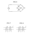
- Reference numeral 1 indicates a traveling conductor; detection coils La and Lb, which are coaxial with conductor 1, and do not make contact with conductor 1, are disposed in a separated manner. Detecting coils La and Lb are connected so as to form the two sides of an alternating current bridge circuit, and in the case in which there is no flaw in the conductor 1 which passes through detecting coils La and Lb, the output signal between terminals a and b is so adjusted as to have a zero balance.
- the detecting coils La and Lb normally produce opposing magnetic fields, so that these magnetic fields repel each other, and it is difficult for the magnetic fields to penetrate sufficiently into the interior of conductor 1, so that the partial detection sensitivity is reduced.
- the detecting coils La and Lb normally produce opposing magnetic fields, so that these magnetic fields repel each other, and it is difficult for the magnetic fields to penetrate sufficiently into the interior of conductor 1, so that the partial detection sensitivity is reduced.
- an object of the present invention to provide an eddy current flaw detection apparatus capable of detecting small flows or small amounts of foreign matter at a high abnormality detection sensitivity.
- the present invention provides an eddy current flow detection apparatus which is characterized by comprising:
- the induction currents produced in the resonance coils by means of the electromagnetic induction from the detection coils are in anti-phase, and the electric current values thereof are equal, so that these induction currents cancel each other out and resonance does not occur.
- Fig. 1 is a circuit diagram showing a preferred embodiment of an eddy current flaw detection apparatus in accordance with the present invention
- a detecting coil L1, a resonance coil L2, a resonance coil L3, and a resonance coil L4 are disposed in that order along a conductor 1 which is traveling from a prior process not depicted in the diagram and coaxial with this conductor, and with gaps therebetween in the axial direction thereof.
- Detecting coils L1 and L2 are identical to those in the conventional apparatus; they comprise alternating current bridge circuit 3 together with the two resistors R1 and R2. The detecting coils are connected differentially so that their magnetic fields are in anti-phase. The resistance of R1 and R2 and the inductance of L1 and L2 are determined so that the alternating current bridge circuit 3 is set to a zero balance state and no signal is generated between nodes A and B when there is no abnormality in conductor 1.
- resonance coils L2 and L3 are identical; they are connected cumulatively, so that the magnetic fields thereof are in phase. These resonance coils L2 and L3 are connected in series to capacity circuit 4 so as to form a resonance circuit.
- the induction current generated by resonance coil L2 by means of the electromagnetic induction of the detecting coil L1 and the induction current generated by resonance coil L3 by means of the electromagnetic induction of the detecting coil L4 are in anti-phase and the electrical current values thereof are equal, so that they are set so as to cancel each other out.
- An oscillator 21, a phase shift circuit 22, a power amplifier 23 and a transformer 24 are provided to constitute an alternating current power source 2 which supplies power to alternating current bridge circuit 3.
- Oscillator 21 generates two periodic signals P1 and P2, which have the same angular frequency w, and the phase angular of P2 is shifted from that of the P1 by 7 r/2.
- Phase shift circuit 22 has an operating member, for example, a volume knob.
- the output signal P of oscillator 21 is supplied to the phase shift circuit 22 to obtain a signal having a phase which is shifted from the phase of the signal P by the phase shift value corresponding to the operation of the operating member.
- the phase shift value can be adjusted in the range of 0 through 7 r by the operation of the operating member.
- the output signal of phase shift circuit 22 is amplified in power amplifier 23.
- the output signal of power amplifier 23 is supplied to one terminal of an input coil of transformer 24.
- the other terminal of the input coil is grounded.
- An output coil of transformer 24 is connected between nodes C and D of the alternating current bridge circuit 3.
- Resistors 31 through 34 and an operational amplifier 35 are provided to constitute a differential amplifier 30 which amplifies the voltage between nodes A and B of alternating current bridge circuit 3.
- the output signal of differential amplifier 30 is supplied to a buffer amplifier 40 to obtain a detection signal.
- phase detection circuits 50 and 60 which have the same function and characteristics are provided.
- the periodic signal P1 and the detection signal S are respectively supplied to first and second input terminals of phase detection circuits 50.
- the periodic signal P2 and the detection signal S are respectively supplied to first and second input terminals of phase detection circuits 60.
- Each phase detection circuit detects a same phase component, which is synchronized with the input signal of the first input terminal, from the input signal of the second input terminal.
- Two low-pass filters 70 and 80 are provided to cut off the higher harmonic components from the output signals of phase detection circuits 70 and 80.
- the output signals of low-pass filters 70 and 80 are supplied respectively to X-axis and Y-axis input terminals of an oscilloscope (not shown).
- Fig. 2 is a circuit diagram showing a concrete example of the capacity circuit 4; this capacity circuit 4 is primarily comprising two operation amplifiers 5 and 6, variable resisters 7 and 8, and condenser 9.
- variable resistor 7 By means of the adjustment of variable resistor 7, it is possible to adjust the resonance frequency of resonance circuit constituted by resonance coils L2 and L3 and capacitance circuit 4, and on the other hand, by means of the adjustment of variable resister 8, it is possible to adjust the resonance Q value of the resonance circuit.
- the present invention is not limited to the circuitry of Fig. 2; it is also possible to construct the capacity circuit by means of simple condensers or variable capacity condensers, and it is also permissible to alter the circuitry in an appropriate manner, when necessary.
- the induction currents generated by resonance coils L2 and L3, by means of the electromagnetic induction from detecting coils L1 and L4 are in anti-phase, and the current values thereof are equal, so that these induction currents cancel each other out and resonance does not occur.
- the detection signal includes a detection component S and a noise signal N.
- the detection component S is generated in response to the change of the impedance of the detecting coil L1 or L4.
- Fig. 3 shows the change of the impedance of the detecting coil.
- the impedance Z of the detecting coil is constituted by the resistance R of that and the reactance " ,L of that, wherein the inductance L includes a intrinsic inductance of the detecting coil and an inductance which is generated by the passage of the flaw or foreign matter.
- the inductance of the detecting coil increases from L to L+ ⁇ L for example.
- Fig. 4 shows an example of detection component S and noise signal N included in a detection signal.
- the phase of the detection component S is shifted from that of the noise signal N by angular q,a' which depends on q)a.
- the detection signal S + N as thus obtained are supplied to the phase detection circuits 50 and 60.
- Components synchronized with the periodic signal P1 are detected from the detection signal S + N by the phase detection circuit 50.
- components synchronized with the periodic signal P2 are detected from the phase detection circuit 60.
- the output signals of the phase detection circuits 50 and 60 are supplied to X-axis and Y-axis input terminals of oscilloscope via low-pass filters 70 and 80.
- vectors corresponding to the detection component S and noise signal N are respectively displayed on the oscilloscope in a distinguishable manner, for example, as shown in Fig. 4.
- an operator adjusts the phase shift value of the phase shift circuit 22 so that the vector of the noise signal S is displayed along X-axis or Y-axis. By this adjustment, the detection component S can be easily distinguished from the noise signal N.
- the detection component S of the detection signal with a greater degree of sensitivity than that possessed by the conventional apparatus, and thus it is possible to improve the detection sensitivity with respect to flaws or foreign matter in the conductor 1.
- the amount of separation of the detecting coils L1 and L4 is increased as a result of the provision of resonance coils L2 and L3, so that the canceling out of the magnetic fields of detecting coils L1 and L4 is reduced, and it is thus possible to increase the sensitivity of the apparatus.
- the inductances of the resonance coils L2 and L3 change and the resonance frequency changes; however, in the present embodiment, by means of the adjustment of the valuable resistor 7 of the capacity circuit 4, it is possible to adjust the resonance frequency of the resonance circuit constituted by the capacity circuit 4 and resonance coils L2 and L3, and it is a simple matter to bring the resonance frequency into agreement with the alternating current power source.
- variable resister 8 it is possible to adjust the resonance Q value, so that, it is possible to alter the Q values of the resonance circuit constituted by the resonance coils L2 and L3 and the capacity circuit 4 in the resonance state and to set the abnormality detection sensitivity at an optimum value.
- the conductor 1 was so disposed as to pass through the coils L1, L2, L3, and L4; however, instead of this, a structure is permissible in which the coils L1, L2, L3, and L4 are enclosed in a casing 10 in a coaxial manner, as shown in Fig. 5, thus forming a measuring element. In this case, the vicinity of the surface of conductor 1 is scanned by means of this measuring element and abnormalities in conductor 1 are thus detected.
Landscapes
- Chemical & Material Sciences (AREA)
- Chemical Kinetics & Catalysis (AREA)
- Electrochemistry (AREA)
- Physics & Mathematics (AREA)
- Health & Medical Sciences (AREA)
- Life Sciences & Earth Sciences (AREA)
- Analytical Chemistry (AREA)
- Biochemistry (AREA)
- General Health & Medical Sciences (AREA)
- General Physics & Mathematics (AREA)
- Immunology (AREA)
- Pathology (AREA)
- Investigating Or Analyzing Materials By The Use Of Magnetic Means (AREA)
Applications Claiming Priority (2)
| Application Number | Priority Date | Filing Date | Title |
|---|---|---|---|
| JP176972/90 | 1990-07-04 | ||
| JP2176972A JP2882856B2 (ja) | 1990-07-04 | 1990-07-04 | 渦流探傷装置 |
Publications (2)
| Publication Number | Publication Date |
|---|---|
| EP0464826A1 true EP0464826A1 (fr) | 1992-01-08 |
| EP0464826B1 EP0464826B1 (fr) | 1995-10-18 |
Family
ID=16022932
Family Applications (1)
| Application Number | Title | Priority Date | Filing Date |
|---|---|---|---|
| EP91111142A Expired - Lifetime EP0464826B1 (fr) | 1990-07-04 | 1991-07-04 | Appareil pour la détection de défauts par courants de Foucault |
Country Status (4)
| Country | Link |
|---|---|
| US (1) | US5146164A (fr) |
| EP (1) | EP0464826B1 (fr) |
| JP (1) | JP2882856B2 (fr) |
| DE (1) | DE69113882T2 (fr) |
Cited By (3)
| Publication number | Priority date | Publication date | Assignee | Title |
|---|---|---|---|---|
| US5329561A (en) * | 1990-06-08 | 1994-07-12 | Framatome | Device for checking the thickness and the cohesion of the interface of a duplex tube |
| FR2773397A1 (fr) * | 1998-01-06 | 1999-07-09 | Intercontrole Sa | Sonde a courants de foucault, pour le controle non destructif de pieces electriquement conductrices |
| EP0884588A4 (fr) * | 1996-10-09 | 2002-05-02 | Mitsubishi Heavy Ind Ltd | Detecteur de defaut par courants de foucault |
Families Citing this family (9)
| Publication number | Priority date | Publication date | Assignee | Title |
|---|---|---|---|---|
| US5485083A (en) * | 1993-10-28 | 1996-01-16 | Smiths Industries | Transformer coupled in-line metallic debris sensor |
| US5514337A (en) * | 1994-01-11 | 1996-05-07 | American Research Corporation Of Virginia | Chemical sensor using eddy current or resonant electromagnetic circuit detection |
| BR0113436A (pt) * | 2000-08-22 | 2004-12-07 | Deere & Co | Método para desenvolver um plano de administração de fazenda, sistema de administração de fazenda, e, programa de computador para gerar um plano de administração de fazenda |
| ES2272796T3 (es) * | 2001-11-02 | 2007-05-01 | Avid Identification Systems, Inc. | Sistema transpondedor con doble arrollamiento de antena. |
| JP4872388B2 (ja) * | 2006-03-10 | 2012-02-08 | 住友電気工業株式会社 | マグネシウム合金用渦電流探傷装置および渦電流探傷方法 |
| JP5592319B2 (ja) | 2011-08-22 | 2014-09-17 | 日立オートモティブシステムズステアリング株式会社 | インテグラル型パワーステアリング装置 |
| US11674927B2 (en) | 2020-01-28 | 2023-06-13 | Tex Riken Co., Ltd. | Eddy current flaw detection apparatus |
| JP7627031B2 (ja) * | 2021-04-20 | 2025-02-05 | テックス理研株式会社 | 渦流探傷装置 |
| CN113640374A (zh) * | 2021-08-05 | 2021-11-12 | 四川德源管道科技股份有限公司 | 用于管道无损检测的涡流检测系统 |
Citations (2)
| Publication number | Priority date | Publication date | Assignee | Title |
|---|---|---|---|---|
| EP0107844A2 (fr) * | 1982-10-21 | 1984-05-09 | Chugoku X-Ray Co., Ltd. | Dispositif de détection de défauts dans les tubes métalliques à l'aide de courants de Foucault |
| EP0315887A2 (fr) * | 1987-11-09 | 1989-05-17 | Nippon Nuclear Fuel Development Co., Ltd. | Appareil et méthode pour la détection de défauts par courant de Foucault |
Family Cites Families (1)
| Publication number | Priority date | Publication date | Assignee | Title |
|---|---|---|---|---|
| GB1567600A (en) * | 1975-10-15 | 1980-05-21 | British Gas Corp | Lipe line inspection equipment |
-
1990
- 1990-07-04 JP JP2176972A patent/JP2882856B2/ja not_active Expired - Lifetime
-
1991
- 1991-07-03 US US07/725,553 patent/US5146164A/en not_active Expired - Lifetime
- 1991-07-04 DE DE69113882T patent/DE69113882T2/de not_active Expired - Lifetime
- 1991-07-04 EP EP91111142A patent/EP0464826B1/fr not_active Expired - Lifetime
Patent Citations (2)
| Publication number | Priority date | Publication date | Assignee | Title |
|---|---|---|---|---|
| EP0107844A2 (fr) * | 1982-10-21 | 1984-05-09 | Chugoku X-Ray Co., Ltd. | Dispositif de détection de défauts dans les tubes métalliques à l'aide de courants de Foucault |
| EP0315887A2 (fr) * | 1987-11-09 | 1989-05-17 | Nippon Nuclear Fuel Development Co., Ltd. | Appareil et méthode pour la détection de défauts par courant de Foucault |
Non-Patent Citations (1)
| Title |
|---|
| PATENT ABSTRACTS OF JAPAN vol. 11, no. 156 (P-578)(2603) 21 May 1987, & JP-A-61 292548 (MITSUBISHI METAL CORP) 23 December 1986, * |
Cited By (3)
| Publication number | Priority date | Publication date | Assignee | Title |
|---|---|---|---|---|
| US5329561A (en) * | 1990-06-08 | 1994-07-12 | Framatome | Device for checking the thickness and the cohesion of the interface of a duplex tube |
| EP0884588A4 (fr) * | 1996-10-09 | 2002-05-02 | Mitsubishi Heavy Ind Ltd | Detecteur de defaut par courants de foucault |
| FR2773397A1 (fr) * | 1998-01-06 | 1999-07-09 | Intercontrole Sa | Sonde a courants de foucault, pour le controle non destructif de pieces electriquement conductrices |
Also Published As
| Publication number | Publication date |
|---|---|
| US5146164A (en) | 1992-09-08 |
| JP2882856B2 (ja) | 1999-04-12 |
| DE69113882D1 (de) | 1995-11-23 |
| JPH0465667A (ja) | 1992-03-02 |
| DE69113882T2 (de) | 1996-04-18 |
| EP0464826B1 (fr) | 1995-10-18 |
Similar Documents
| Publication | Publication Date | Title |
|---|---|---|
| US8278918B2 (en) | Method for operating of a metal detection system and metal detection system | |
| US5146164A (en) | Eddy current flaw detection apparatus employing a resonance circuit | |
| US3826973A (en) | Electromagnetic gradiometer | |
| US7061236B2 (en) | Metal detector | |
| US6541963B2 (en) | Differential eddy-current transducer | |
| GB2146128A (en) | Metal detection apparatus | |
| KR0163959B1 (ko) | 와류탐상 장치 | |
| JPH0672783B2 (ja) | 信号形成装置 | |
| CN115004022B (zh) | 涡流探伤装置 | |
| US12013264B2 (en) | Position sensing apparatus and method | |
| NL1012710C2 (nl) | Werkwijze voor het vergelijken van, of het meten van de verschillen tussen, twee of meer elektrische impedanties. | |
| JPS637634B2 (fr) | ||
| JP3809635B2 (ja) | コイルの銅抵抗補償回路 | |
| US2429336A (en) | Electromagnetic testing | |
| JPH0587944A (ja) | 金属検出装置 | |
| JPS637633B2 (fr) | ||
| JP2024147929A (ja) | 磁気検出システム | |
| JP2002022709A (ja) | 渦流探傷装置 | |
| JP2638419B2 (ja) | Mri装置の直交型rfコイル | |
| JPH07333020A (ja) | 電磁流量計 | |
| JPS6125281B2 (fr) | ||
| JPH0534218A (ja) | トルク測定装置の温度補償装置 | |
| Yu et al. | Eddy current microsensor for use in micromachine applications | |
| JPS6332157B2 (fr) | ||
| JPH055510Y2 (fr) |
Legal Events
| Date | Code | Title | Description |
|---|---|---|---|
| PUAI | Public reference made under article 153(3) epc to a published international application that has entered the european phase |
Free format text: ORIGINAL CODE: 0009012 |
|
| AK | Designated contracting states |
Kind code of ref document: A1 Designated state(s): DE GB |
|
| 17P | Request for examination filed |
Effective date: 19920518 |
|
| 17Q | First examination report despatched |
Effective date: 19941230 |
|
| GRAA | (expected) grant |
Free format text: ORIGINAL CODE: 0009210 |
|
| AK | Designated contracting states |
Kind code of ref document: B1 Designated state(s): DE GB |
|
| REF | Corresponds to: |
Ref document number: 69113882 Country of ref document: DE Date of ref document: 19951123 |
|
| PLBE | No opposition filed within time limit |
Free format text: ORIGINAL CODE: 0009261 |
|
| STAA | Information on the status of an ep patent application or granted ep patent |
Free format text: STATUS: NO OPPOSITION FILED WITHIN TIME LIMIT |
|
| 26N | No opposition filed | ||
| REG | Reference to a national code |
Ref country code: GB Ref legal event code: IF02 |
|
| PGFP | Annual fee paid to national office [announced via postgrant information from national office to epo] |
Ref country code: DE Payment date: 20100723 Year of fee payment: 20 |
|
| PGFP | Annual fee paid to national office [announced via postgrant information from national office to epo] |
Ref country code: GB Payment date: 20100722 Year of fee payment: 20 |
|
| REG | Reference to a national code |
Ref country code: DE Ref legal event code: R071 Ref document number: 69113882 Country of ref document: DE |
|
| REG | Reference to a national code |
Ref country code: DE Ref legal event code: R071 Ref document number: 69113882 Country of ref document: DE |
|
| REG | Reference to a national code |
Ref country code: GB Ref legal event code: PE20 Expiry date: 20110703 |
|
| PG25 | Lapsed in a contracting state [announced via postgrant information from national office to epo] |
Ref country code: GB Free format text: LAPSE BECAUSE OF EXPIRATION OF PROTECTION Effective date: 20110703 |
|
| PG25 | Lapsed in a contracting state [announced via postgrant information from national office to epo] |
Ref country code: DE Free format text: LAPSE BECAUSE OF EXPIRATION OF PROTECTION Effective date: 20110705 |