EP0465079B1 - Procédé et dispositif d'attribution d'adresses entrée/sortie dans un appareil de traitement de données - Google Patents
Procédé et dispositif d'attribution d'adresses entrée/sortie dans un appareil de traitement de données Download PDFInfo
- Publication number
- EP0465079B1 EP0465079B1 EP91305701A EP91305701A EP0465079B1 EP 0465079 B1 EP0465079 B1 EP 0465079B1 EP 91305701 A EP91305701 A EP 91305701A EP 91305701 A EP91305701 A EP 91305701A EP 0465079 B1 EP0465079 B1 EP 0465079B1
- Authority
- EP
- European Patent Office
- Prior art keywords
- address
- port
- data
- additional
- standard
- Prior art date
- Legal status (The legal status is an assumption and is not a legal conclusion. Google has not performed a legal analysis and makes no representation as to the accuracy of the status listed.)
- Expired - Lifetime
Links
Images

Classifications
-
- G—PHYSICS
- G06—COMPUTING OR CALCULATING; COUNTING
- G06F—ELECTRIC DIGITAL DATA PROCESSING
- G06F12/00—Accessing, addressing or allocating within memory systems or architectures
- G06F12/02—Addressing or allocation; Relocation
- G06F12/06—Addressing a physical block of locations, e.g. base addressing, module addressing, memory dedication
- G06F12/0646—Configuration or reconfiguration
- G06F12/0684—Configuration or reconfiguration with feedback, e.g. presence or absence of unit detected by addressing, overflow detection
Definitions
- the present invention relates to a data processing apparatus and, more particularly, to a method and a device for assigning I/O address in a data processing apparatus which is capable of changing the assignment of the address to an I/O port.
- Printer RS-232C, floppy disk drive (FDD), hard disk drive (HDD), etc. are connected to personal computers and the like through standard ports. Since the number of standard ports is different depending upon the demand of the user, the main unit of a personal computer is generally provided with an extension slot (I/O slot) and a standard port is added by inserting an additional board provided with a standard port into the I/O slot.
- I/O slot extension slot
- an additional board generally has a DIP switch for setting the address of the standard port thereon, and it is possible to change the I/O address of the standard port on the additional board by operating the DIP switch, thereby preventing the conflict of both standard ports.
- such an additional board is provided with a connecting portion 1 which is connected to the main unit, a decoder 2, a standard port 3 and a DIP switch 4.
- An address signal supplied from the main unit through an address bus A is input to the decoder 2.
- the decoder 2 supplies a decoding signal (chip selecting signal CS ) indicating that the standard port 3 is selected to the standard port 3.
- the I/O address which is to be assigned to the standard port 3 is determined in accordance with the I/O device which is to be connected to the standard port 3. There are two addresses, for example, a primary address and a secondary address for one I/O device.
- the decoder 2 can decode either of the addresses.
- the DIP switch 4 is connected to the decoder 2, and the decoder 2 can select the I/O address to be decoded in response to the turning on and off of the DIP switch 4.
- a connector 3a connects the additional board to an external device such as a printer.
- the DIP switch 4 When the address of the standard port 3 on the additional board is actually assigned, the DIP switch 4 is operated so as to prevent the coincidence of the address of the standard port 3 on the additional board and the address of the standard port in the main unit, thereby preventing the conflict of both standard ports.
- EP-A-0350917 discloses a personal computer system in which the presence is detected of optional Read Only Memory having a start address which conflicts with the start address of existing Read Only Memory, so that the existing ROM can be reassigned to non-conflicting address space.
- the existing ROM On power-on, the existing ROM is disabled and data is read at the start address. If the readout data coincides with predetermined data which would be present at the start address of optional ROM, the presence of optional ROM is confirmed and the existing ROM assigned to a different start address in non-conflicting address space.
- IBM Technical Disclosure Bulletin Vol.22, No.10, March 1980 pages 4366-4368 discloses performing a Write/Read operation at the known address of an optional feature card to check that the feature card is present and functional.
- the present invention provides an I/O address assigning device in a data processing apparatus having a first I/O port for connecting the data processing apparatus to an I/O device, said first I/O port having an I/O address assignable from a plurality of standard I/O port addresses, and an I/O connecting portion for connecting an additional I/O port to the data processing apparatus, wherein any said additional I/O port has a preset I/O address assigned from said plurality of standard I/O addresses, and a data register to which data for said additional I/O port can be written and from which data can be read, the I/O address assigning device comprising:
- the present invention also provides a method of assigning an I/O address in a data processing apparatus having a first I/O port for connecting the data processing apparatus to an I/O device, said first I/O port having an I/O address assignable from a plurality of standard I/O port addresses, and an I/O connecting portion for connecting an additional I/O port to the data processing apparatus, wherein any said additional I/O port has a preset I/O address assigned from said plurality of standard I/O addresses, and a data register to which data for said additional I/O port can be written and from which data can be read, the method comprising the steps of:
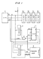
- Fig. 1 is a block diagram of the entire structure of an embodiment of the present invention. These elements are provided in the main unit. To a CPU 5 are connected an address bus A supplying an address signal of 16-bits (A0 to A15) which indicates what is to be accessed therethrough, a control bus C for supplying an operation command such as IOW, IOR, MEMR and MEMW therethrough, and a data bus supplying data of 8 bits (D0 to D7) therethrough.
- A supplying an address signal of 16-bits (A0 to A15) which indicates what is to be accessed therethrough
- a control bus C for supplying an operation command such as IOW, IOR, MEMR and MEMW therethrough
- D0 to D7 data bus supplying data of 8 bits
- the I/O address assigning device in a data processing apparatus of this embodiment is provided with four I/O slots 6a to 6d into which an additional board can be inserted.
- Each of the address bus A, the control bus C and the data bus D is connected to these I/O slots. Since all the bits of the data bus D are pulled up by a pullup means Vp, when there is no data on the data bus D, the data bus D becomes FFH (all "1").
- the address bus A is connected to the input terminal of a decoder 7.
- the decoder 7 outputs a decoding signal (chip selecting signal CS ) indicating that a standard port 8 is selected to the standard port 8 when the address of the address bus A reaches a predetermined value (e.g., 278H).
- the output terminal of the decoder 7 is connected to the input terminal of the standard port 8 in the main unit, and when the chip selecting signal CS is [L], the standard port 8 in the main unit inputs or outputs data.
- the data bus D and the control bus C are also connected to the standard port 8 in the main unit.
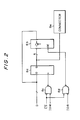
- the standard port 8 in the main unit is provided with a data register 8a to which the data bus D is connected so as to enable data reading and writing, a buffer 8b for judging whether or not the output of the register 8a is to be returned to the data bus D, an OR gate 8c for issuing a data-fetch command when a write command is issued, an OR gate 8d for allowing the buffer 8b to output data when a read command is issued, and a connector 8e for connecting the standard port 8 to an external device, as shown in Fig. 2.
- the value of the address bus A reaches the address of the standard port 8 in the main unit and the chip selecting signal CS from the decoder 7 becomes [L]. Since the signal IOW from the control bus C becomes [L] in accordance with the write command, the OR gate 8c outputs [L] and the register 8a fetches the data from the data bus D.
- the chip selecting signal CS from the decoder 7 becomes [L] as in the case of the write command. Since the signal IOR from the control bus C becomes [L] in accordance with the read command, the OR gate 8d outputs [L].
- the buffer 8b is allowed to output data, and the output of the register 8a is supplied to the data bus D. In this way, the CPU 5 can both write desired data into the register 8a of the standard port 8 in the main unit and read the data from the register 8a.
- This embodiment is provided with a decoder 9, an OR gate 10 and an address switching register 11 of 2 bits.
- the address bus A is connected to the input terminal of the decoder 9 and when the value of the address bus A reaches a predetermined value, the decoder 9 outputs [L].
- the output of the decoder 9 is input to the OR gate 10 together with the signal IOW from the control bus C.
- the address switching register 11 is composed of two flip-flops, namely, an enable bit 11a and an address select bit 11b.
- the output of the OR gate 10 is input to the clock input terminals of the two flip-flops 11a, 11b, and 2 bits (D0, D1) of the data bus D are connected to the data input terminals of the enable bit 11a and the address select bit 11b, respectively.
- the decoder 9 When the CPU 5 issues a write command while addressing the address switching register 11, the decoder 9 outputs [L].
- the signal IOW from the control bus C becomes [L] in accordance with the write command, and the output of the OR gate 10 also becomes [L]. Therefore, the data of the buses D0 and D1 are fetched into the enable bit 11a and the address select bit 11b, respectively, of the address switching register 11.
- the outputs of the enable bit 11a and the address select bit 11b of the address switching register 11 are supplied to the decoder 7 as an enabling signal and an address selecting signal, respectively.
- the decoder 7 has a gate on the output side which does not output [L] unless the enabling signal is [L]. In other words, it is possible to so control the decoder 7 as to write/read data into/from the standard port 8 in the main unit in correspondence with the data stored in the enable bit 11a.
- the decoder 7 has a gate on the input side which outputs [L] as the chip selecting signal CS at a primary address (e.g., [278H]) when the address selecting signal of the address switching register 11 is [H] and outputs [L] as the chip selecting signal CS at a secondary address (e.g., [378H]) when the address selecting signal of the address switching register 11 is [L]. It is therefore possible to change the I/O address at which [L] is output as the chip selecting signal CS from the decoder 7 by the data which is stored in the address select bit 11b.
- a primary address e.g., [278H]
- a secondary address e.g., [378H]
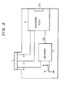
- the concrete structure of the decoder 7 is shown in Fig. 3.
- the decoder 7 is composed of a NAND gate 7a for decoding the primary address, a NAND gate 7b for decoding the secondary address, an AND gate 7c and an OR gate 7d.
- the address on the address bus A and the address selecting signal from the address select bit 11b of the address switching register 11 are supplied to the NAND gate 7a, while the address on the address bus A and the address selecting signal from the address select bit 11b of the address switching register 11 are supplied to the NAND gate 7b in the inverted form. Therefore, when the address on the address bus A is the primary address and the address selecting signal is [H], the NAND gate 7a outputs [L]. On the other hand, when the address on the address bus A is the secondary address and the address selecting signal is [L], the NAND gate 7b outputs [L]. In the other cases, both NAND gates 7a, 7b output [H].
- the outputs of the NAND gates 7a, 7b are input to the AND gate 7c. Therefore, when the output of either of the NAND gates 7a, 7b is [L], the AND gate 7c outputs [L].
- To the OR gate 7d are supplied the output of the AND gate 7c and the enable signal from the enable bit 11a of the address switching register 11. Therefore, only when the enable signal is [L] and the output of the AND gate 7c is [L], [L] is output as the chip selecting signal CS . In this way, the above-described operation is achieved.
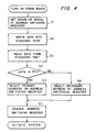
- the access to the standard port 8 in the main board is inhibited at S1. Since the data bus D is pulled up by the pullup means Vp, the data read out is [FFH] unless an additional board provided with a standard port to which the primary address is assigned is inserted into any of the I/O slots 6a to 6d. If the additional board provided with a standard port is inserted into the I/O slot, the data written at S2 is read out.
- the address of the standard port 8 in the main unit is set at the primary address.
- the address of the standard port 8 in the main unit is set at the secondary address.
- the address select bit 11b has 1 bit and two kinds of addresses are switched over to each other, but it is possible to increase the number of addresses switched by increasing the number of bits of the address select bit 11b.
- the standard port in this embodiment is for a printer, it may be an I/O address assigning device for an external FDD (floppy disk drive), an RS-232C (an interface for transmitting serial data) or the like.
- FDD floppy disk drive
- RS-232C an interface for transmitting serial data
- an I/O address assigning device of a data processing apparatus of this embodiment of the present invention it is possible not only to inhibit the access to the I/O port in the apparatus but also to automatically change the assignment of the I/O address. That is, it is possible to identify the address of another I/O port added thereto and set the address of the original I/O port at an address which prevents conflict of both I/O ports.
Landscapes
- Engineering & Computer Science (AREA)
- Theoretical Computer Science (AREA)
- Physics & Mathematics (AREA)
- General Engineering & Computer Science (AREA)
- General Physics & Mathematics (AREA)
- Bus Control (AREA)
- Programmable Controllers (AREA)
- Information Transfer Systems (AREA)
Claims (6)
- Dispositif d'affectation d'adresse d'entrée/sortie dans un dispositif de traitement de données compointant un premier point d'entrée/sortie (8) pour connecter le dispositif de traitement de données à un dispositif d'entrée/sortie, ledit premier point d'entrée/sortie (8) compointant une adresse d'entrée/sortie pouvant être affectée depuis une pluralité d'adresses de points d'entrée/sortie standard, et une partie de connexion d'entrée/sortie (6a, 6b, 6c, 6d) pour connecter un point d'entrée/sortie additionnel (3) au dispositif de traitement de données, dans lequel n'impointe lequel desdits points d'entrée/sortie additionnels (3) a une adresse d'entrée/sortie prédéterminée affectée à partir de ladite pluralité d'adresses d'entrée/sortie standard, et un registre de données (8a) dans lequel des données pour ledit point d'entrée/sortie additionnel (3) peuvent être écrites et depuis lequel des données peuvent être lues, le dispositif d'affectation d'adresse d'entrée/sortie comprenant :des moyens de commande (11a, 7d) pour invalider le premier point d'entrée/sortie (8) ;des moyens de détection (5) pour détecter l'adresse d'entrée/sortie prédéterminée d'un point d'entrée/sortie additionnel (3) connecté à la partie de connexion d'entrée/sortie (6a, 6b, 6c, 6d) pendant que le premier point d'entrée/sortie (8) est invalidé, lesdits moyens de détection comprenant :des moyens de lecture et d'écriture (5, 8a, 8b, 8c, 8d) pour écrire, et, ensuite, pour lire des données sur une adresse de point d'entrée/sortie standard prédéterminée ; etdes moyens de détection d'identité (5) pour détecter si les données lues sur l'adresse de point d'entrée/sortie standard prédéterminée ont une identité avec les données écrites sur ladite adresse, de façon à déterminer si ladite adresse de point d'entrée/sortie standard prédéterminée est l'adresse d'entrée/sortie prédéterminée d'un point d'entrée/sortie additionnel (3) connecté à la partie de connexion d'entrée/sortie (6a, 6b, 6c, 6d) ; etdes moyens d'affectation (7, 9, 10, 11b) pour générer un signal de commutation d'adresse pour configurer le premier point d'entrée/sortie (8) de façon à effectuer une commutation avec une adresse d'entrée/sortie qui est différente de ladite adresse d'entrée/sortie prédéterminée détectée par les moyens de détection (5) et valider ledit premier point d'entrée/sortie (8).
- Dispositif d'affectation d'adresse d'entrée/sortie selon la revendication 1, dans lequel les moyens de commande (lla, 7d) comprennent :(a) un registre d'état invalidé (11a) dans lequel des données désignant un état invalidé sont établies ; et(b) des moyens (7d) pour invalider un signal de sélection de puce devant être délivré au premier point d'entrée/sortie (8) en fonction de la sortie du registre d'état invalidé (11a).
- Dispositif d'affectation d'adresse d'entrée/sortie selon l'une ou l'autre des revendications 1 ou 2, dans lequel les moyens d'affectation (7, 9, 10, 11b) comprennent :(a) un registre d'adresse d'entrée/sortie (11b) dans lequel est établie une information concernant celle de la pluralité d'adresses d'entrée/sortie qui est sélectionnée; et(b) un décodeur d'adresse (7) pour recevoir un signal d'adresse et délivrer en sortie un signal de sélection de puce au premier point d'entrée/sortie (8) lorsque l'adresse d'entrée est une adresse d'entrée/sortie qui correspond à l'information établie dans le registre d'adresse d'entrée/sortie (11b).
- Dispositif d'affectation d'adresse d'entrée/sortie selon l'une quelconque des revendications précédentes, dans lequel les moyens de commande (11a, 7d), les moyens de détection (5) et les moyens d'affectation (7, 9, 10, 11b) sont démarrés lorsqu'une source d'alimentation en énergie pour le dispositif de traitement de données est mise en service.
- Dispositif d'affectation d'adresse d'entrée/sortie selon l'une quelconque des revendications précédentes, dans lequel les moyens d'affectation (7, 9, 10, 11b) affectent ladite adresse de point d'entrée/sortie standard prédéterminée au premier point d'entrée/sortie (8) lorsque ladite identité n'est pas détectée par les moyens de détection d'identité (5).
- Procédé d'affectation d'une adresse d'entrée/sortie dans un dispositif de traitement de données compointant un premier point d'entrée/sortie (8) pour connecter le dispositif de traitement de données à un dispositif d'entrée/sortie, ledit premier point d'entrée/sortie (8) compointant une adresse d'entrée/sortie pouvant être affectée à partir d'une pluralité d'adresses de points d'entrée/sortie standard, et une partie de connexion d'entrée/sortie (6a, 6b, 6c, 6d) pour connecter un point d'entrée/sortie additionnel (3) au dispositif de traitement de données, dans lequel n'impointe lequel desdits points d'entrée/sortie additionnels (3) compointe une adresse d'entrée/sortie prédéterminée affectée à partir de ladite pluralité d'adresses d'entrée/sortie standard, et un registre de données (8a) dans lequel des données pour ledit point d'entrée/sortie additionnel (3) peuvent être écrites et depuis lequel des données peuvent être lues, le procédé comprenant les étapes suivantes :l'invalidation du premier point d'entrée/sortie (8) ;la détection de l'adresse d'entrée/sortie prédéterminée d'un point d'entrée/sortie additionnel (3) connecté à la partie de connexion d'entrée/sortie (6a, 6b, 6c, 6d) lorsque le premier point d'entrée/sortie (8) est invalidé, ladite étape de détection comprenant les étapes suivantes :l'écriture, et, ensuite, la lecture, de données sur une adresse de point d'entrée/sortie standard prédéterminée ; etla détection du fait que les données lues sur l'adresse de point d'entrée/sortie standard prédéterminée présentent une identité avec les données écrites sur ladite adresse, afin de déterminer si ladite adresse de point d'entrée/sortie standard prédéterminée est l'adresse d'entrée/sortie prédéterminée d'un point d'entrée/sortie additionnel (3) connecté à la partie de connexion d'entrée/sortie (6a, 6b, 6c, 6d) ;la configuration du premier point d'entrée/sortie (8) de façon à effectuer une commutation vers une adresse d'entrée/sortie qui est différente de ladite adresse d'entrée/sortie prédéterminée détectée par les moyens de détection (5) ; etla validation dudit premier point d'entrée/sortie (8).
Applications Claiming Priority (3)
| Application Number | Priority Date | Filing Date | Title |
|---|---|---|---|
| JP2171845A JP2547654B2 (ja) | 1990-06-29 | 1990-06-29 | データ処理装置 |
| JP17184590 | 1990-06-29 | ||
| JP171845/90 | 1990-06-29 |
Publications (3)
| Publication Number | Publication Date |
|---|---|
| EP0465079A2 EP0465079A2 (fr) | 1992-01-08 |
| EP0465079A3 EP0465079A3 (fr) | 1992-01-29 |
| EP0465079B1 true EP0465079B1 (fr) | 1999-12-08 |
Family
ID=15930837
Family Applications (1)
| Application Number | Title | Priority Date | Filing Date |
|---|---|---|---|
| EP91305701A Expired - Lifetime EP0465079B1 (fr) | 1990-06-29 | 1991-06-24 | Procédé et dispositif d'attribution d'adresses entrée/sortie dans un appareil de traitement de données |
Country Status (4)
| Country | Link |
|---|---|
| US (1) | US5301276A (fr) |
| EP (1) | EP0465079B1 (fr) |
| JP (1) | JP2547654B2 (fr) |
| DE (1) | DE69131823T2 (fr) |
Families Citing this family (22)
| Publication number | Priority date | Publication date | Assignee | Title |
|---|---|---|---|---|
| FR2687489A1 (fr) * | 1992-02-13 | 1993-08-20 | Hewlett Packard Co | Bus de connexion de cartes d'extension a un systeme informatique et procede de test. |
| US5454078A (en) * | 1992-08-07 | 1995-09-26 | International Business Machines Corporation | System for sharing name among network adapters by, dynamically linking adapters having same logical name and maintaining linked state of remaining adapters |
| US5561813A (en) * | 1993-08-27 | 1996-10-01 | Advanced System Products, Inc. | Circuit for resolving I/O port address conflicts |
| GB2288953B (en) * | 1994-03-21 | 1998-08-05 | Peter Wolstenholme | Self-testing secure-transaction computer input-output bus |
| US5596728A (en) * | 1994-05-04 | 1997-01-21 | Compaq Computer Corporation | Method and apparatus for resolving resource conflicts after a portable computer has docked to an expansion base unit |
| US5787306A (en) * | 1994-05-18 | 1998-07-28 | National Semiconductor Corporation | Automatic assignment of I/O addresses in a computer system |
| JPH0830306A (ja) * | 1994-07-12 | 1996-02-02 | Rika Kogyo Kk | 制御装置 |
| DE4426294A1 (de) * | 1994-07-26 | 1996-02-01 | Michael Dr Gude | Adreß-Selktionsschaltung für PC-Karten |
| JP2691140B2 (ja) * | 1994-09-28 | 1997-12-17 | インターナショナル・ビジネス・マシーンズ・コーポレイション | 情報処理装置及びその制御方法 |
| US5634075A (en) * | 1995-01-11 | 1997-05-27 | Cirrus Logic, Inc. | Backward compatibility for plug and play systems |
| US5787305A (en) * | 1995-04-25 | 1998-07-28 | Pc-Tel, Inc. | Host signal processing modem using a software simulation of a UART |
| US5566304A (en) * | 1995-05-08 | 1996-10-15 | Apple Computer, Inc. | Method of dynamic selection between immediate and delayed read access acknowledgement |
| US5781796A (en) * | 1995-06-06 | 1998-07-14 | Lg Semicon Co., Ltd. | System for automatic configuration of I/O base address without configuration program using readout data on common bus by responding device |
| US5832280A (en) * | 1995-10-05 | 1998-11-03 | International Business Machines Corporation | Method and system in a data processing system for interfacing an operating system with a power management controller. |
| US5802306A (en) * | 1995-10-31 | 1998-09-01 | International Business Machines Corporation | Supporting multiple client-server sessions from a protocol stack associated with a single physical adapter through use of a plurality of logical adapters |
| US5664221A (en) * | 1995-11-14 | 1997-09-02 | Digital Equipment Corporation | System for reconfiguring addresses of SCSI devices via a device address bus independent of the SCSI bus |
| JPH09179810A (ja) * | 1995-12-25 | 1997-07-11 | Matsushita Electric Works Ltd | ユニット選択装置 |
| DE19618802A1 (de) * | 1996-05-10 | 1997-11-13 | Kremer Merseburg Horst | Schnittstellenansteuerung |
| US5938776A (en) * | 1997-06-27 | 1999-08-17 | Digital Equipment Corporation | Detection of SCSI devices at illegal locations |
| US6820148B1 (en) * | 2000-08-17 | 2004-11-16 | Sandisk Corporation | Multiple removable non-volatile memory cards serially communicating with a host |
| TWI244594B (en) * | 2004-07-13 | 2005-12-01 | Quanta Comp Inc | Method for automatically assigning the address of communication ports and a blade server system |
| CN1877537A (zh) * | 2005-06-10 | 2006-12-13 | 鸿富锦精密工业(深圳)有限公司 | 外围部件互连设备信息识别系统及方法 |
Family Cites Families (9)
| Publication number | Priority date | Publication date | Assignee | Title |
|---|---|---|---|---|
| US4556953A (en) * | 1982-02-24 | 1985-12-03 | Caprio A Ronald | Interchangeable interface circuitry arrangements for use with a data processing system |
| JPS60214063A (ja) * | 1984-04-09 | 1985-10-26 | Nec Corp | 情報処理装置 |
| US4775931A (en) * | 1984-05-11 | 1988-10-04 | Hewlett-Packard Company | Dynamically configured computing device |
| US4760553A (en) * | 1985-06-03 | 1988-07-26 | International Business Machines Corporation | Terminal system configuration tracing method and apparatus |
| DE3683778D1 (de) * | 1986-10-30 | 1992-03-12 | Ibm | Datenverarbeitungsanordnung mit vorrichtungen zur automatischen adresszuordnung zur adressierung von schnittstellenmodulen. |
| US5038320A (en) * | 1987-03-13 | 1991-08-06 | International Business Machines Corp. | Computer system with automatic initialization of pluggable option cards |
| JPS63289661A (ja) * | 1987-05-22 | 1988-11-28 | Oki Electric Ind Co Ltd | 入出力装置のアドレス割付け方法 |
| US4964038A (en) * | 1987-10-28 | 1990-10-16 | International Business Machines Corp. | Data processing system having automatic address allocation arrangements for addressing interface cards |
| JPH0223440A (ja) * | 1988-07-13 | 1990-01-25 | Toshiba Corp | パーソナルコンピュータ |
-
1990
- 1990-06-29 JP JP2171845A patent/JP2547654B2/ja not_active Expired - Lifetime
-
1991
- 1991-06-17 US US07/715,998 patent/US5301276A/en not_active Expired - Fee Related
- 1991-06-24 DE DE69131823T patent/DE69131823T2/de not_active Expired - Fee Related
- 1991-06-24 EP EP91305701A patent/EP0465079B1/fr not_active Expired - Lifetime
Also Published As
| Publication number | Publication date |
|---|---|
| JP2547654B2 (ja) | 1996-10-23 |
| US5301276A (en) | 1994-04-05 |
| JPH0460857A (ja) | 1992-02-26 |
| DE69131823D1 (de) | 2000-01-13 |
| EP0465079A2 (fr) | 1992-01-08 |
| DE69131823T2 (de) | 2000-04-06 |
| EP0465079A3 (fr) | 1992-01-29 |
Similar Documents
| Publication | Publication Date | Title |
|---|---|---|
| US5301276A (en) | Method and device for assigning I/O address in data processing apparatus | |
| US4964038A (en) | Data processing system having automatic address allocation arrangements for addressing interface cards | |
| US5724529A (en) | Computer system with multiple PC card controllers and a method of controlling I/O transfers in the system | |
| US5881252A (en) | Method and apparatus for automatically configuring circuit cards in a computer system | |
| US5038320A (en) | Computer system with automatic initialization of pluggable option cards | |
| US5109517A (en) | System for selectively controlling slots in an IBM-AT/NEC 9801 dual-compatible computer | |
| US5687346A (en) | PC card and PC card system with dual port ram and switchable rewritable ROM | |
| CN1063564A (zh) | 可泊接便携式计算机的自动设备配置 | |
| US6298408B1 (en) | Intelligent input and output controller for flexible interface | |
| US4849931A (en) | Data processing system having interfacing circuits assigned to a common I/O port address by utilizing a specific bit line of a common bus | |
| CA2084133C (fr) | Ordinateur a carte d'adaptation automatique | |
| US5222218A (en) | System with devices connected in sequence to receive information in a predetermined order | |
| US6598157B1 (en) | Dynamic boot block control by boot configuration determination and subsequent address modification | |
| JPS63116258A (ja) | デ−タ処理システム | |
| EP0653704A1 (fr) | Dispositif et procédé de configuration des cartes d'expansion dans un ordinateur | |
| US5594879A (en) | Method of and apparatus for arbitrarily disabling under processor control individual slots on a computer bus | |
| US5168562A (en) | Method and apparatus for determining the allowable data path width of a device in a computer system to avoid interference with other devices | |
| US5751998A (en) | Memory accessing system with portions of memory being selectively write protectable and relocatable based on predefined register bits and memory selection RAM outputs | |
| US5561813A (en) | Circuit for resolving I/O port address conflicts | |
| JP4083474B2 (ja) | メモリ装置の制御方法およびそのプログラムならびに記録媒体 | |
| US5786885A (en) | Image processing system | |
| US5797032A (en) | Bus for connecting extension cards to a data processing system and test method | |
| KR970004521B1 (ko) | 컴퓨터 입출력(i/o)보드 제어장치 | |
| KR950007107B1 (ko) | 별도의 마이크로프로세서를 포함하는 컴퓨터장치 | |
| KR900006547B1 (ko) | 컴퓨터용 메모리 구성장치 |
Legal Events
| Date | Code | Title | Description |
|---|---|---|---|
| PUAI | Public reference made under article 153(3) epc to a published international application that has entered the european phase |
Free format text: ORIGINAL CODE: 0009012 |
|
| PUAL | Search report despatched |
Free format text: ORIGINAL CODE: 0009013 |
|
| AK | Designated contracting states |
Kind code of ref document: A2 Designated state(s): DE FR GB |
|
| AK | Designated contracting states |
Kind code of ref document: A3 Designated state(s): DE FR GB |
|
| 17P | Request for examination filed |
Effective date: 19920327 |
|
| 17Q | First examination report despatched |
Effective date: 19941205 |
|
| GRAG | Despatch of communication of intention to grant |
Free format text: ORIGINAL CODE: EPIDOS AGRA |
|
| GRAG | Despatch of communication of intention to grant |
Free format text: ORIGINAL CODE: EPIDOS AGRA |
|
| GRAH | Despatch of communication of intention to grant a patent |
Free format text: ORIGINAL CODE: EPIDOS IGRA |
|
| GRAH | Despatch of communication of intention to grant a patent |
Free format text: ORIGINAL CODE: EPIDOS IGRA |
|
| GRAA | (expected) grant |
Free format text: ORIGINAL CODE: 0009210 |
|
| AK | Designated contracting states |
Kind code of ref document: B1 Designated state(s): DE FR GB |
|
| REF | Corresponds to: |
Ref document number: 69131823 Country of ref document: DE Date of ref document: 20000113 |
|
| ET | Fr: translation filed | ||
| PLBE | No opposition filed within time limit |
Free format text: ORIGINAL CODE: 0009261 |
|
| STAA | Information on the status of an ep patent application or granted ep patent |
Free format text: STATUS: NO OPPOSITION FILED WITHIN TIME LIMIT |
|
| 26N | No opposition filed | ||
| REG | Reference to a national code |
Ref country code: GB Ref legal event code: IF02 |
|
| PGFP | Annual fee paid to national office [announced via postgrant information from national office to epo] |
Ref country code: FR Payment date: 20030610 Year of fee payment: 13 |
|
| PGFP | Annual fee paid to national office [announced via postgrant information from national office to epo] |
Ref country code: GB Payment date: 20030618 Year of fee payment: 13 |
|
| PGFP | Annual fee paid to national office [announced via postgrant information from national office to epo] |
Ref country code: DE Payment date: 20030707 Year of fee payment: 13 |
|
| PG25 | Lapsed in a contracting state [announced via postgrant information from national office to epo] |
Ref country code: GB Free format text: LAPSE BECAUSE OF NON-PAYMENT OF DUE FEES Effective date: 20040624 |
|
| PG25 | Lapsed in a contracting state [announced via postgrant information from national office to epo] |
Ref country code: DE Free format text: LAPSE BECAUSE OF NON-PAYMENT OF DUE FEES Effective date: 20050101 |
|
| GBPC | Gb: european patent ceased through non-payment of renewal fee |
Effective date: 20040624 |
|
| PG25 | Lapsed in a contracting state [announced via postgrant information from national office to epo] |
Ref country code: FR Free format text: LAPSE BECAUSE OF NON-PAYMENT OF DUE FEES Effective date: 20050228 |
|
| REG | Reference to a national code |
Ref country code: FR Ref legal event code: ST |