EP0465138A2 - Interconnexion de composants électroniques - Google Patents
Interconnexion de composants électroniques Download PDFInfo
- Publication number
- EP0465138A2 EP0465138A2 EP91305850A EP91305850A EP0465138A2 EP 0465138 A2 EP0465138 A2 EP 0465138A2 EP 91305850 A EP91305850 A EP 91305850A EP 91305850 A EP91305850 A EP 91305850A EP 0465138 A2 EP0465138 A2 EP 0465138A2
- Authority
- EP
- European Patent Office
- Prior art keywords
- alignment
- layer
- conductors
- conductor
- dielectric material
- Prior art date
- Legal status (The legal status is an assumption and is not a legal conclusion. Google has not performed a legal analysis and makes no representation as to the accuracy of the status listed.)
- Withdrawn
Links
Images





Classifications
-
- H—ELECTRICITY
- H10—SEMICONDUCTOR DEVICES; ELECTRIC SOLID-STATE DEVICES NOT OTHERWISE PROVIDED FOR
- H10W—GENERIC PACKAGES, INTERCONNECTIONS, CONNECTORS OR OTHER CONSTRUCTIONAL DETAILS OF DEVICES COVERED BY CLASS H10
- H10W70/00—Package substrates; Interposers; Redistribution layers [RDL]
- H10W70/60—Insulating or insulated package substrates; Interposers; Redistribution layers
- H10W70/611—Insulating or insulated package substrates; Interposers; Redistribution layers for connecting multiple chips together
-
- H—ELECTRICITY
- H10—SEMICONDUCTOR DEVICES; ELECTRIC SOLID-STATE DEVICES NOT OTHERWISE PROVIDED FOR
- H10W—GENERIC PACKAGES, INTERCONNECTIONS, CONNECTORS OR OTHER CONSTRUCTIONAL DETAILS OF DEVICES COVERED BY CLASS H10
- H10W70/00—Package substrates; Interposers; Redistribution layers [RDL]
- H10W70/60—Insulating or insulated package substrates; Interposers; Redistribution layers
-
- H—ELECTRICITY
- H10—SEMICONDUCTOR DEVICES; ELECTRIC SOLID-STATE DEVICES NOT OTHERWISE PROVIDED FOR
- H10W—GENERIC PACKAGES, INTERCONNECTIONS, CONNECTORS OR OTHER CONSTRUCTIONAL DETAILS OF DEVICES COVERED BY CLASS H10
- H10W70/00—Package substrates; Interposers; Redistribution layers [RDL]
- H10W70/60—Insulating or insulated package substrates; Interposers; Redistribution layers
- H10W70/611—Insulating or insulated package substrates; Interposers; Redistribution layers for connecting multiple chips together
- H10W70/614—Insulating or insulated package substrates; Interposers; Redistribution layers for connecting multiple chips together the multiple chips being integrally enclosed
-
- H—ELECTRICITY
- H10—SEMICONDUCTOR DEVICES; ELECTRIC SOLID-STATE DEVICES NOT OTHERWISE PROVIDED FOR
- H10W—GENERIC PACKAGES, INTERCONNECTIONS, CONNECTORS OR OTHER CONSTRUCTIONAL DETAILS OF DEVICES COVERED BY CLASS H10
- H10W70/00—Package substrates; Interposers; Redistribution layers [RDL]
- H10W70/60—Insulating or insulated package substrates; Interposers; Redistribution layers
- H10W70/67—Insulating or insulated package substrates; Interposers; Redistribution layers characterised by their insulating layers or insulating parts
- H10W70/68—Shapes or dispositions thereof
- H10W70/685—Shapes or dispositions thereof comprising multiple insulating layers
Definitions
- the present invention relates to the inter-connection of electronic components.
- Illustrative embodiments of the invention relate to electronic systems and to high density interconnect structures, and more particularly, to accommodation of chip placement tolerances in such systems.
- a high density interconnect (HDI) structure or system which has been developed by General Electric Company offers many advantages in the compact assembly of electronic systems.
- an electronic system such as a micro computer which incorporates 30-50 chips can be fully assembled and interconnected-on a single substrate which is 2 inch long by 2 inch wide by .050 inch thick.
- this interconnect structure can be disassembled for repair or replacement of a faulty component and then reassembled without significant risk to the good components incorporated within the system. This is particularly important where as many as 50 chips having a cost of as much as $2,000.00, each, may be incorporated in a single system on one substrate.
- This repairability is a substantial advance over prior connection systems in which reworking the system to replace damaged components was either impossible or involved substantial risk to the good components.
- a ceramic substrate such as alumina which may be 100 mils thick and of appropriate size and strength for the overall system, is provided. This size is typically less than 2 inches square, but may be made larger or smaller.
- individual cavities or one large cavity having appropriate depth at the intended locations of differing chips is prepared. This may be done by starting with a bare substrate having a uniform thickness and the desired size. Conventional, ultrasonic or laser milling may be used to form the cavities in which the various chips and other components will be positioned. For many systems where it is desired to place chips nearly edge-to-edge, a single large cavity is satisfactory. That large cavity may typically have a uniform depth where the semiconductor chips have a substantially uniform thickness.
- the cavity bottom may be made respectively deeper or shallower to place the upper surface of the corresponding component in substantially the same plane as the upper surface of the rest of the components and the portion of the substrate which surrounds the cavity.
- the bottom of the cavity is then provided with a thermoplastic adhesive layer which may preferably be polyetherimide resin available under the trade name ULTEM® 6000 from the General Electric Company.
- the various components are then placed in their desired locations within the cavity, the entire structure is heated to about 300°C which is above the softening point of the ULTEM® polyetherimide (which is in the vicinity of 235°C) and then cooled to thermoplastically bond the individual components to the substrate.
- RIE reactive ion etching
- the substrate and chips
- a metallization layer which is deposited over the Kapton® layer extends into the via holes and makes electrical contact to the contact pads disposed thereunder.
- This metallization layer may be patterned to form individual conductors during the process of depositing it or may be deposited as a continuous layer and then patterned using photoresist and etching.
- the photoresist is preferably exposed using a laser to provide an accurately aligned conductor pattern at the end of the process. Alternatively, exposure through a mask may be used.
- the entire interconnect structure can be fabricated from start to finish (after definition of the required conductor patterns and receipt of the electronic components) in as little as ⁇ 8-12 hours.
- This high density interconnect structure provides many advantages. Included among these are the the lightest weight and smallest volume packaging of such an electronic system presently available. A further, and possibly more significant advantage of this high density interconnect structure, is the short time required to design and fabricate a system using this high density interconnect structure.
- Prior art processes require the prepackaging of each semiconductor chip, the design of a multilayer circuit board to interconnect the various packaged chips, and so forth. Multilayer circuit boards are expensive and require substantial lead time for their fabrication. In contrast, the only thing which must be specially pre-fabricated for the HDI system is the substrate on which the individual semiconductor chips will be mounted.
- This substrate is a standard stock item, other than the requirement that the substrate have appropriate cavities therein for the placement of the semiconductor chips so that the interconnect surface of the various chips and the substrate will be in a single plane.
- the required cavities may be formed in an already fired ceramic substrate by conventional or laser milling. This milling process is straightforward and fairly rapid with the result that once a desired configuration for the substrate has been established, a corresponding physical substrate can be made ready for the mounting of the semiconductor chips in as little as 1 day and typically 4 hours for small quantities as are suitable for research or prototype systems to confirm the design prior to quantity production.
- the process of designing an interconnection pattern for interconnecting all of the chips and components of an electronic system on a single high density interconnect substrate normally takes somewhere between one week and five weeks. Once that interconnect structure has been defined, assembly of the system on the substrate may begin. First, the chips are mounted on the substrate and the overlay structure is built-up on top of the chips and substrate, one layer at a time. Typically, the entire process can be finished in one day and in the event of a high priority rush, could be completed in four hours. Consequently, this high density interconnect structure not only results in a substantially lighter weight and more compact package for an electronic system, but enables a prototype of the system to be fabricated and tested in a much shorter time than is required with other packaging techniques.
- This high density interconnect system is now being used for the interconnection of fairly complex systems including 40 to 60 chips which are interconnected by 1500 to 3000 nodes with the result that a computerized router typically requires relatively long runs (of from 10 to 24 hours) to successfully route all the interconnections and, in some cases, is unable to route some of the interconnections when using only two signal layers.
- each metallization layer and the via holes in each dielectric layer must either be individually tailored to the exact positions of the various integrated circuit chips (as placed) or an adaptive lithography system must adjust an ideal metallization and via hole pattern in accordance with the actual position of the various integrated circuit chips.
- this problem is solved by adaptation of an ideal metallization pattern in accordance with the actual location of each of the integrated circuits chips and its contact pads by modifying the metallization pattern to properly connect to those contact pads in their actual positions. That adaptation is enabled by providing a "picture frame" around the allowed location of each integrated circuit chip in which adaptation of the metal layer takes place.
- one of the design rules for the ideal metallization is that each metal path which crosses a picture frame must do so perpendicular to those sides of that picture frame which it crosses.
- the ideal metallization pattern over each chip is maintained with respect to the chip and thus, must be shifted and/or rotated with respect to the portion of the metallization pattern outside the picture frame in accordance with any shift and/or rotation of the chip with respect to its ideal location.
- the ideal metallization pattern outside the outer edges of the picture frames is maintained with respect to the substrate, i.e. unchanged during the adaptation process.
- Adaptation to the actual location of each chip is accomplished by modifying the metallization pattern within the picture frame area for that chip to properly connect from the ideal metallization pattern at the outside edge of that picture frame to the shifted/rotated ideal metallization pattern over that chip. This results in the angling of conductors within its picture frame when the chip is displaced perpendicular to, or rotated with respect to its ideal position relative to a side of the picture frame.
- Illustrative embodiments of the invention disclosed herein seek: to accommodate tolerances in chip placement in a high density interconnect structure in a manner which places no restrictions on either the signal conductor layers or the routing system; to avoid any adaptation of the signal conductor layers of a high density interconnect structure in accommodating chip placement tolerances; to provide full accommodation for chip placement tolerances in a first, non-signal conductor layer of a high density interconnect structure; to accommodate chip placement tolerances in a ground plane layer and a power plane layer of high density interconnect structures which include such layers; and/or to permit routing of increasing complexity structures without requiring excessive routing time.
- One alignment conductor is associated with each contact pad which is to be connected to the high density interconnect structure.
- that misplacement may be compensated for merely by adjusting the placement of the via hole which connects the overlying signal conductor to that alignment conductor or the alignment conductor's position may also to be adapted in order to position the alignment conductor where that via hole can properly overlap that alignment conductor and be properly overlapped by that signal conductor.
- This alignment conductor layer of the high density interconnect structure may preferably be a ground plane in order to provide shielding between the chips and the overlying signal conductors, and to provide the low voltage drops necessary in order for the system to operate at its maximum possible speed and in order to avoid "wasting" a conductor layer of the high density interconnect structure by dedicating it exclusively to alignment conductors.
- alignment conductors in the first two conductive layers of the high density interconnect structure.
- two layers of alignment conductors should be sufficient to accommodate all acceptable placement tolerances. However, more layers of alignment conductors may be employed, if necessary.
- the alignment conductors serve to provide, for every chip connection, a conductor connected to the chip contact pad which is positioned where the first signal layer via hole, when properly positioned with respect to a fixed, non-adapted signal conductor pattern, will be aligned over that conductor.
- the signal conductor layer has a fixed pattern which is merely aligned with a fixed pattern of via holes which expose those conductors. This enables the signal layer and the via holes for them to be patterned without any adaptation. These layers may be patterned using pre-fabricated standard masks.
- a portion of a high density interconnect structure 10 is illustrated in plan view.
- the illustrated portion includes a corner of a chip 16 having square chip contact pads 18 along two sides of the chip.
- a signal conductor 50 comprises a conductive run or trace 52 and an enlarged cover pad 58 where it connects to a conductor in a lower level through a via hole.
- Alignment conductors 30 and 40 may also be referred to as alignment correction conductors since their positions can be shifted to provide a connection path between a cover pad 58 and its associated contact pad when the cover pad and the contact pad are offset or otherwise disposed out of ideal alignment.
- the first level alignment conductors 30 are indicated by a dashed line outline so that they may be distinguished from the underlying contact pads which are shown in solid outline and the overlying conductors.
- the second level alignment conductors 40 are illustrated in a dotted outline in the plan view in Figure 1 and the signal conductors are illustrated in a solid outline since their small dimensions makes them distinguishable from the underlying solid outline of the contact pads.
- the signal conductor pattern and the contact pad pattern are illustrated in their ideal alignment in which the cover pads 58 of the signal conductors are centered over the contact pads 18.
- the alignment conductors 30 and 40 are preferably 6 mils by 12 mils, that is one and one-half times the length of a side of a contact pad by three times the length of a side of a contact pad.
- the alignment conductors 30 and 40 are disposed in alignment with each other.
- Conductors 40 are drawn slightly smaller than conductors 30 in order that the boundaries of each will be visible in the figures.
- conductors 30 and 40 are the same size in an actual structure.
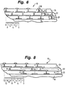
- Figure 2 is a stylized, cross-section of the Figure 1 structure through the row of contact pads 18 along the top of Figure 1.
- Figure 2 includes a portion of the high density interconnect structure substrate 12 on which the chips 16 are disposed, at least during high density interconnect structure fabrication. No section line is shown in Figure 1 because the section is taken in different places for different conductor layers.
- Each conductor's cross-section is taken in the plane of the via which connects it to next lower conductor in order to clearly illustrate the manner in which the contact pad 18 of the chip is connected by its associated first and second alignment conductors (30 and 40, respectively) to its associated signal conductor 50.
- the via portion of the signal conductor which extends downward from the cover pad 58 is identified by the reference numeral 54.
- the via portion of the alignment conductors 30 and 40 are identified by the reference numerals 34 and 44, respectively.
- the via holes may be directly stacked, if such stacking is permitted by design rules. We prefer to space them apart as indicated in the plan view in Figure 1 where each circle represents one or more vias located at that point in plan view.
- the vias in the first layer of dielectric material (which are part of the first conductor layer and thus the alignment conductors 30) are identified in the plan view by a capital " A ".
- the vias in the second layer of dielectric material (which are part of the second conductor layer and thus the alignment conductors 40) are identified in the plan view by a capital ".
- the vias in the third layer of dielectric material are identified in the plan view by a capital " C ".
- the circles labeled " A+C” indicate the location in plan view of a via 34 and a via 54 which are vertically aligned, although not directly connected.
- the circles labeled “ B” indicate the location in plan view of a via 44. These letter designations are used for the vias associated with the right-most contact pad 18 in Figure 2.
- the displacement of the via B from the vias A and C avoids the creation of dimples in the high density interconnect structure which can occur if two vias in adjacent layers are stacked one on top of another.
- dielectric layer 22 fills in any depression in the first layer via 34 ( A ) thereby providing a planar surface for the metallization 40 to which the via 54 ( C ).
- FIG. 1 is only a small portion of a much larger, multi-chip system which is interconnected by the high density interconnect structure 10, a portion of which is illustrated in Figure 1.
- the actual placement of each of the chips in that larger system will be in its own unique position with its own deviation from the ideal desired position for that chip.
- the ideal alignment between cover pads of the signal layer and the contact pads of the chip will not be present at most of the chips in the structure and may not be present at any of the chips in the structure.
- the position of the signal conductor layer relative to the contact pads of any particular chip 16 is determined by an overall best fit alignment of the signal conductor pattern to the actual position of every chip involved in the structure.
- This position of the signal layer may be in its ideal position relative to the substrate on which the individual chips are disposed or may have some other position. However, for each chip, that chip will have some particular displacement from its ideal position relative to the overlying signal conductor pattern.
- the displacement between the chip's contact pads 18 and the cover pads 58 of the signal conductor layer are phrased in terms of the displacement of the chip contact pads relative to the signal conductor layer. This is because the signal conductor layer extends across the whole structure and thus serves as a single common reference with respect to which all displacements can be expressed.
- the position in which the signal layer will be placed is first determined. Then, positions are selected for the first and second alignment conductors in which the first alignment conductor 30 overlaps a contact pad 18 by a sufficient amount for a via connection to be formed between that alignment conductor and that contact pad.
- a position for the second alignment conductor 40 is selected which provides sufficient overlap between it and the first alignment conductor 30 to allow a via hole connecting them to be properly positioned in that overlap, while at the same time, positioning that second alignment conductor 40 in a position where the signal conductor cover pad 58, which is to be connected to the contact pad in question, is disposed completely over the second alignment conductor such that it can be connected thereto by a proper via.
- the specific locations for the alignment conductors are adapted in accordance with actual chip placement and are determined based on the known, but not yet placed position of the signal conductor layer and the known and already placed, actual positions of the chip's contact pads.
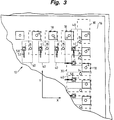
- Figures 3 and 4 illustrate a situation in which the contact pads 18 are displaced relative to the cover pads 58 of the signal conductors by +7 mils in the X-direction and +7 mils in the Y-direction.
- the lower alignment conductors 30 (away from the corner) are shifted relative to the contact pads 18 to place the contact pads 18, which are disposed along the top of the chip, so that they are just completely overlapped by the upper right-hand corner of the first level alignment conductors 30.
- the second level alignment conductors 40 are displaced downward to the left so that they provide a 2 mil overlay in the X-direction with the alignment conductors 30, as shown in Figure 3.
- the alignment conductors 40 could be positioned at the same Y-direction Position as the alignment conductor 30.
- Each alignment conductor 40 is just fully overlapped by the cover pad 58 of its associated signal conductor 50 at the left-hand side of the alignment conductors 40.
- the first level via connections are centered in the contact pads 18 as indicated by the circles A .
- the second level vias between the first and second alignment conductors are centered in their overlap in the X-direction as indicated by the circles B .
- the third level vias between the signal conductor cover pads 58 and the second alignment conductors 40 are centered in the cover pads 58 as indicated by the circles C .
- a scale is provided indicating the distance by which the center of the left-most signal conductor cover pad 58 is displaced from the center of its associated chip contact pad 18. In this configuration, that distance is 7 mils. This is the maximum displacement which can be handled using rectangular alignment conductors of the sizes indicated while still having the first level alignment conductors 30 fully overlapping the chip contact pads 18 as may be considered desirable to ensure that the first level via holes do not extend off the contact pads 18.
- the repeating pattern of the alignment conductor positioning and the alignment conductors standard size are adjusted to provide a connection between each cover pad 58 and its associated contact pad 18 without introducing short circuits. For small misalignments, such variations in the alignment conductor pattern can be avoided.
- the pattern for the top corner contact pad 18 and the top corner cover pad 58 could be repeated for each of the other top contact pads.
- the first level alignment conductors 30, which are disposed outward from the contact pads, are illustrated in dashed lines and are elevated above the other first level alignment conductors in order to clearly illustrate the manner of the connection between the cover pads 58 and the contact pads 18.
- the first level metallization which includes the first alignment conductors, serves as a ground plane in the high density interconnect structure and is substantially continuous except in the vicinity of the alignment conductors where a gap is left to isolate them from the ground plane.
- This continuous portion of the ground plane is not illustrated for the sake of drawing clarity.
- the second layer of metallization in this structure is preferably a power plane which is substantially continuous except in the vicinity of the second level alignment conductors which, again, are spaced from the rest of the power plane to provide isolation.
- both the portion of the first level metallization which is disposed within the area bounded by the contact pads of a single chip and the portion which is outside that boundary are connected together as much as possible in view of the design rules, the number and placement of contact pads on the chip and the number of ground or power contact pads on the chip, in order that each may be substantially continuous. This facilitates minimizing the voltage drop in the power and ground planes and thereby maximizes the speed at which the system can operate.
- the L-shaped first level alignment conductors 30 effectively prevent the placing of a connection between the portion of that layer which is disposed over the center of the chip and the portion of that layer which is disposed outside the contact pads of the chip along the top of the chip except at isolated locations where a connection therebetween can be provided because one of the contact pads connects directly to that layer or because of a gap in the contact pad pattern or the presence of a contact pad which is not connected to the high density interconnect structure.
- This blockage is a result of the portion of an L-shaped alignment conductor disposed outside the contact pads overlapping the gap between two L-shaped alignment conductors disposed on the inside of the contact pads. This difficulty can be alleviated to some extent by the alternate configuration for the pads of figures 7 and 8 which is illustrated in figures 9 and 10.
- connection path between each contact pad and the cover pad of its associated signal conductor has the same configuration in plan view as it does in Figure 7.
- the contact pads whose connection runs outside the chip contact pad pattern it is the first level alignment conductor which is rectangular and it is the second level alignment conductor which is L-shaped.
- This has the effect of providing space for a straight-through conductor run in the gaps between adjacent L-shaped alignment conductors in each of the conductor levels.
- the use of such L-shaped alignment conductors should be unnecessary with the result that this solution to this problem is not expected to be needed except under rare conditions unless the size and center-to-center spacing of chip contact pads is significantly reduced.
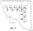
- alignment conductors which are restricted to a single layer of the high density interconnect structure.
- Such a structure is illustrated at 10′ in Figures 11 and 12 in which 6 mils square alignment conductors 30 ⁇ are employed in a system having 4 mils square chip pads disposed on 8 mils centers.
- the alignment conductors are displaced relative to the contact pads so that only a 2 x 2 mils overlap is provided.
- a misposition of up to 5 mils in either direction may be corrected in a single layer of alignment conductors.
- it is preferably a ground plane, as has been described above.
Landscapes
- Production Of Multi-Layered Print Wiring Board (AREA)
- Structures For Mounting Electric Components On Printed Circuit Boards (AREA)
Applications Claiming Priority (2)
| Application Number | Priority Date | Filing Date | Title |
|---|---|---|---|
| US07/545,793 US5357403A (en) | 1990-06-29 | 1990-06-29 | Adaptive lithography in a high density interconnect structure whose signal layers have fixed patterns |
| US545793 | 1990-06-29 |
Publications (1)
| Publication Number | Publication Date |
|---|---|
| EP0465138A2 true EP0465138A2 (fr) | 1992-01-08 |
Family
ID=24177570
Family Applications (1)
| Application Number | Title | Priority Date | Filing Date |
|---|---|---|---|
| EP91305850A Withdrawn EP0465138A2 (fr) | 1990-06-29 | 1991-06-27 | Interconnexion de composants électroniques |
Country Status (3)
| Country | Link |
|---|---|
| US (1) | US5357403A (fr) |
| EP (1) | EP0465138A2 (fr) |
| JP (1) | JPH04233256A (fr) |
Cited By (5)
| Publication number | Priority date | Publication date | Assignee | Title |
|---|---|---|---|---|
| EP0610631A1 (fr) * | 1992-12-28 | 1994-08-17 | AT&T GLOBAL INFORMATION SOLUTIONS INTERNATIONAL INC. | Connecteur électrique |
| EP0662713A3 (fr) * | 1993-12-14 | 1995-08-30 | Ibm | Zones de contactminimisées appliquées à des trous de contact dans les substrats en céramique. |
| EP1259103A4 (fr) * | 2000-02-25 | 2004-07-28 | Ibiden Co Ltd | Carte a circuits imprimes multicouche et procede de production d'une carte a circuits imprimes multicouche |
| WO2005015634A1 (fr) * | 2003-07-28 | 2005-02-17 | Infineon Technologies Ag | Procede d'application d'un cablage sur un flan, permettant une compensation des defauts de positionnement des puces a semi-conducteur dans les positions des composants du flan |
| US7852634B2 (en) | 2000-09-25 | 2010-12-14 | Ibiden Co., Ltd. | Semiconductor element, method of manufacturing semiconductor element, multi-layer printed circuit board, and method of manufacturing multi-layer printed circuit board |
Families Citing this family (22)
| Publication number | Priority date | Publication date | Assignee | Title |
|---|---|---|---|---|
| US5573428A (en) * | 1994-06-24 | 1996-11-12 | Motorola, Inc. | Hermetic electrical connector |
| JP2964981B2 (ja) * | 1997-03-14 | 1999-10-18 | 日本電気株式会社 | 半導体装置 |
| US6118137A (en) * | 1997-09-08 | 2000-09-12 | Advanced Micro Devices, Inc. | Test structure responsive to electrical signals for determining lithographic misalignment of conductors relative to vias |
| US6756295B2 (en) * | 1998-12-21 | 2004-06-29 | Megic Corporation | Chip structure and process for forming the same |
| US6965165B2 (en) | 1998-12-21 | 2005-11-15 | Mou-Shiung Lin | Top layers of metal for high performance IC's |
| US6936531B2 (en) * | 1998-12-21 | 2005-08-30 | Megic Corporation | Process of fabricating a chip structure |
| US6181004B1 (en) | 1999-01-22 | 2001-01-30 | Jerry D. Koontz | Digital signal processing assembly and test method |
| US7107673B2 (en) * | 2000-06-19 | 2006-09-19 | Nortel Networks Limited | Technique for accommodating electronic components on a multiplayer signal routing device |
| US20030102159A1 (en) * | 2001-12-04 | 2003-06-05 | Loo Mike C. | Optimum power and ground bump pad and bump patterns for flip chip packaging |
| US7932603B2 (en) | 2001-12-13 | 2011-04-26 | Megica Corporation | Chip structure and process for forming the same |
| US6876088B2 (en) | 2003-01-16 | 2005-04-05 | International Business Machines Corporation | Flex-based IC package construction employing a balanced lamination |
| US7253510B2 (en) * | 2003-01-16 | 2007-08-07 | International Business Machines Corporation | Ball grid array package construction with raised solder ball pads |
| US6867121B2 (en) * | 2003-01-16 | 2005-03-15 | International Business Machines Corporation | Method of apparatus for interconnecting a relatively fine pitch circuit layer and adjacent power plane(s) in a laminated construction |
| US6864171B1 (en) * | 2003-10-09 | 2005-03-08 | Infineon Technologies Ag | Via density rules |
| US7316512B2 (en) * | 2004-07-30 | 2008-01-08 | General Electric Company | Interconnect device |
| JP2009135147A (ja) * | 2007-11-28 | 2009-06-18 | Shinko Electric Ind Co Ltd | 配線基板及び電子素子の接続構造及び電子装置 |
| US20120222721A1 (en) | 2011-03-02 | 2012-09-06 | General Electric Company | Photovoltaic module package and fabrication method |
| JP5754507B2 (ja) * | 2011-06-21 | 2015-07-29 | 株式会社村田製作所 | 回路モジュール |
| TWI642334B (zh) * | 2017-10-25 | 2018-11-21 | 欣興電子股份有限公司 | 電路板及其製造方法 |
| TWI642333B (zh) | 2017-10-25 | 2018-11-21 | 欣興電子股份有限公司 | 電路板及其製造方法 |
| US10678150B1 (en) | 2018-11-15 | 2020-06-09 | Applied Materials, Inc. | Dynamic generation of layout adaptive packaging |
| US11934762B2 (en) | 2021-08-06 | 2024-03-19 | Applied Materials, Inc. | Overlaying on locally dispositioned patterns by ML based dynamic digital corrections (ML-DDC) |
Family Cites Families (8)
| Publication number | Priority date | Publication date | Assignee | Title |
|---|---|---|---|---|
| US3705332A (en) * | 1970-06-25 | 1972-12-05 | Howard L Parks | Electrical circuit packaging structure and method of fabrication thereof |
| US4349862A (en) * | 1980-08-11 | 1982-09-14 | International Business Machines Corporation | Capacitive chip carrier and multilayer ceramic capacitors |
| FR2556503B1 (fr) * | 1983-12-08 | 1986-12-12 | Eurofarad | Substrat d'interconnexion en alumine pour composant electronique |
| FR2567684B1 (fr) * | 1984-07-10 | 1988-11-04 | Nec Corp | Module ayant un substrat ceramique multicouche et un circuit multicouche sur ce substrat et procede pour sa fabrication |
| US4628406A (en) * | 1985-05-20 | 1986-12-09 | Tektronix, Inc. | Method of packaging integrated circuit chips, and integrated circuit package |
| US4874721A (en) * | 1985-11-11 | 1989-10-17 | Nec Corporation | Method of manufacturing a multichip package with increased adhesive strength |
| JPS63181400A (ja) * | 1987-01-22 | 1988-07-26 | 松下電器産業株式会社 | セラミツク多層基板 |
| US4954878A (en) * | 1989-06-29 | 1990-09-04 | Digital Equipment Corp. | Method of packaging and powering integrated circuit chips and the chip assembly formed thereby |
-
1990
- 1990-06-29 US US07/545,793 patent/US5357403A/en not_active Expired - Fee Related
-
1991
- 1991-06-19 JP JP3173316A patent/JPH04233256A/ja not_active Withdrawn
- 1991-06-27 EP EP91305850A patent/EP0465138A2/fr not_active Withdrawn
Cited By (29)
| Publication number | Priority date | Publication date | Assignee | Title |
|---|---|---|---|---|
| EP0610631A1 (fr) * | 1992-12-28 | 1994-08-17 | AT&T GLOBAL INFORMATION SOLUTIONS INTERNATIONAL INC. | Connecteur électrique |
| EP0662713A3 (fr) * | 1993-12-14 | 1995-08-30 | Ibm | Zones de contactminimisées appliquées à des trous de contact dans les substrats en céramique. |
| US5916451A (en) * | 1993-12-14 | 1999-06-29 | International Business Machines Corporation | Minimal capture pads applied to ceramic vias in ceramic substrates |
| US8186045B2 (en) | 2000-02-25 | 2012-05-29 | Ibiden Co., Ltd. | Multilayer printed circuit board and multilayer printed circuit board manufacturing method |
| US8046914B2 (en) | 2000-02-25 | 2011-11-01 | Ibiden Co., Ltd. | Method for manufacturing multilayer printed circuit board |
| EP1814154A1 (fr) * | 2000-02-25 | 2007-08-01 | Ibiden Co., Ltd. | Carte à circuits imprimés multicouche et procédé de production d'une carte à circuits imprimés multicouche |
| US7435910B2 (en) | 2000-02-25 | 2008-10-14 | Ibiden Co., Ltd. | Multilayer printed circuit board |
| US8453323B2 (en) | 2000-02-25 | 2013-06-04 | Ibiden Co., Ltd. | Printed circuit board manufacturing method |
| EP1990833A3 (fr) * | 2000-02-25 | 2010-09-29 | Ibiden Co., Ltd. | Carte de circuit imprimé multicouche et son procédé de fabrication |
| US7842887B2 (en) | 2000-02-25 | 2010-11-30 | Ibiden Co., Ltd. | Multilayer printed circuit board |
| US8438727B2 (en) | 2000-02-25 | 2013-05-14 | Ibiden Co., Ltd. | Multilayer printed circuit board and multilayer printed circuit board manufacturing method |
| EP1259103A4 (fr) * | 2000-02-25 | 2004-07-28 | Ibiden Co Ltd | Carte a circuits imprimes multicouche et procede de production d'une carte a circuits imprimes multicouche |
| US7884286B2 (en) | 2000-02-25 | 2011-02-08 | Ibiden Co., Ltd. | Multilayer printed circuit board |
| US7888605B2 (en) | 2000-02-25 | 2011-02-15 | Ibiden Co., Ltd. | Multilayer printed circuit board |
| US7888606B2 (en) | 2000-02-25 | 2011-02-15 | Ibiden Co., Ltd. | Multilayer printed circuit board |
| US8079142B2 (en) | 2000-02-25 | 2011-12-20 | Ibiden Co., Ltd. | Printed circuit board manufacturing method |
| US7908745B2 (en) | 2000-09-25 | 2011-03-22 | Ibiden Co., Ltd. | Method of manufacturing multi-layer printed circuit board |
| US7999387B2 (en) | 2000-09-25 | 2011-08-16 | Ibiden Co., Ltd. | Semiconductor element connected to printed circuit board |
| US8067699B2 (en) | 2000-09-25 | 2011-11-29 | Ibiden Co., Ltd. | Semiconductor element, method of manufacturing semiconductor element, multi-layer printed circuit board, and method of manufacturing multi-layer printed circuit board |
| US7893360B2 (en) | 2000-09-25 | 2011-02-22 | Ibiden Co., Ltd. | Semiconductor element, method of manufacturing semiconductor element, multi-layer printed circuit board, and method of manufacturing multi-layer printed circuit board |
| US7855342B2 (en) | 2000-09-25 | 2010-12-21 | Ibiden Co., Ltd. | Semiconductor element, method of manufacturing semiconductor element, multi-layer printed circuit board, and method of manufacturing multi-layer printed circuit board |
| US8293579B2 (en) | 2000-09-25 | 2012-10-23 | Ibiden Co., Ltd. | Semiconductor element, method of manufacturing semiconductor element, multi-layer printed circuit board, and method of manufacturing multi-layer printed circuit board |
| US7852634B2 (en) | 2000-09-25 | 2010-12-14 | Ibiden Co., Ltd. | Semiconductor element, method of manufacturing semiconductor element, multi-layer printed circuit board, and method of manufacturing multi-layer printed circuit board |
| US8524535B2 (en) | 2000-09-25 | 2013-09-03 | Ibiden Co., Ltd. | Semiconductor element, method of manufacturing semiconductor element, multi-layer printed circuit board, and method of manufacturing multi-layer printed circuit board |
| US8822323B2 (en) | 2000-09-25 | 2014-09-02 | Ibiden Co., Ltd. | Semiconductor element, method of manufacturing semiconductor element, multi-layer printed circuit board, and method of manufacturing multi-layer printed circuit board |
| US8959756B2 (en) | 2000-09-25 | 2015-02-24 | Ibiden Co., Ltd. | Method of manufacturing a printed circuit board having an embedded electronic component |
| US9245838B2 (en) | 2000-09-25 | 2016-01-26 | Ibiden Co., Ltd. | Semiconductor element |
| WO2005015634A1 (fr) * | 2003-07-28 | 2005-02-17 | Infineon Technologies Ag | Procede d'application d'un cablage sur un flan, permettant une compensation des defauts de positionnement des puces a semi-conducteur dans les positions des composants du flan |
| US7514273B2 (en) | 2003-07-28 | 2009-04-07 | Qimonda Ag | Method for applying rewiring to a panel while compensating for position errors of semiconductor chips in component positions of the panel |
Also Published As
| Publication number | Publication date |
|---|---|
| US5357403A (en) | 1994-10-18 |
| JPH04233256A (ja) | 1992-08-21 |
Similar Documents
| Publication | Publication Date | Title |
|---|---|---|
| US5357403A (en) | Adaptive lithography in a high density interconnect structure whose signal layers have fixed patterns | |
| EP0305398B1 (fr) | Agencement d'interconnexion de plusieurs circuits integres | |
| US5258920A (en) | Locally orientation specific routing system | |
| EP1158570B1 (fr) | Procédé d'interconnexion verticale pour segments en silicium | |
| US4991000A (en) | Vertically interconnected integrated circuit chip system | |
| US5216806A (en) | Method of forming a chip package and package interconnects | |
| US5200810A (en) | High density interconnect structure with top mounted components | |
| CA1236926A (fr) | Methode et structure permettant d'apporter des modification dans un module a plusieurs dispositifs | |
| US5019997A (en) | Adaptive lithography accommodation of tolerances in chip positioning in high density interconnection structures | |
| EP0073149B1 (fr) | Module de montage pour puce semi-conductrice | |
| US5386627A (en) | Method of fabricating a multi-layer integrated circuit chip interposer | |
| US4982265A (en) | Semiconductor integrated circuit device and method of manufacturing the same | |
| US5876842A (en) | Modular circuit package having vertically aligned power and signal cores | |
| US4862249A (en) | Packaging system for stacking integrated circuits | |
| US5459634A (en) | Area array interconnect device and method of manufacture thereof | |
| EP0465196A2 (fr) | Structure d'interconnexion compacte à haute densité | |
| EP0465195A2 (fr) | Procédé d'interconnexion à haute densité et à laminage multipe et structure utilisant des adhésifs thermoplastiques avec des Tg's qui diminuent successivement | |
| EP0329133A2 (fr) | Substrat renversé pour puce | |
| US4649417A (en) | Multiple voltage integrated circuit packaging substrate | |
| EP0341001B1 (fr) | Procédé de réalisation de dispositifs semi-conducteurs de grande dimension | |
| JPH0393258A (ja) | デイスクリートチップを使用した3次元集積回路構成 | |
| JPH05243481A (ja) | パッケージ型電子システム及び気密パッケージ型電子システム | |
| US4920454A (en) | Wafer scale package system and header and method of manufacture thereof | |
| US6955944B2 (en) | Fabrication method for a semiconductor CSP type package | |
| EP0795906A2 (fr) | Assemblage de circuits électroniques et procédé de fabrication associé |
Legal Events
| Date | Code | Title | Description |
|---|---|---|---|
| PUAI | Public reference made under article 153(3) epc to a published international application that has entered the european phase |
Free format text: ORIGINAL CODE: 0009012 |
|
| AK | Designated contracting states |
Kind code of ref document: A2 Designated state(s): DE FR GB IT |
|
| 18W | Application withdrawn |
Withdrawal date: 19920221 |
|
| STAA | Information on the status of an ep patent application or granted ep patent |
Free format text: STATUS: THE APPLICATION HAS BEEN WITHDRAWN |
|
| R18W | Application withdrawn (corrected) |
Effective date: 19920221 |