EP0466134A2 - Methode und Vorrichtung zum passiven Ausrichten von Diodenlasern und optischen Fasern - Google Patents
Methode und Vorrichtung zum passiven Ausrichten von Diodenlasern und optischen Fasern Download PDFInfo
- Publication number
- EP0466134A2 EP0466134A2 EP91111501A EP91111501A EP0466134A2 EP 0466134 A2 EP0466134 A2 EP 0466134A2 EP 91111501 A EP91111501 A EP 91111501A EP 91111501 A EP91111501 A EP 91111501A EP 0466134 A2 EP0466134 A2 EP 0466134A2
- Authority
- EP
- European Patent Office
- Prior art keywords
- chip
- substrate
- contact
- laser
- pedestals
- Prior art date
- Legal status (The legal status is an assumption and is not a legal conclusion. Google has not performed a legal analysis and makes no representation as to the accuracy of the status listed.)
- Granted
Links
Images


Classifications
-
- H—ELECTRICITY
- H01—ELECTRIC ELEMENTS
- H01S—DEVICES USING THE PROCESS OF LIGHT AMPLIFICATION BY STIMULATED EMISSION OF RADIATION [LASER] TO AMPLIFY OR GENERATE LIGHT; DEVICES USING STIMULATED EMISSION OF ELECTROMAGNETIC RADIATION IN WAVE RANGES OTHER THAN OPTICAL
- H01S5/00—Semiconductor lasers
- H01S5/40—Arrangement of two or more semiconductor lasers, not provided for in groups H01S5/02 - H01S5/30
- H01S5/4025—Array arrangements, e.g. constituted by discrete laser diodes or laser bar
-
- G—PHYSICS
- G02—OPTICS
- G02B—OPTICAL ELEMENTS, SYSTEMS OR APPARATUS
- G02B6/00—Light guides; Structural details of arrangements comprising light guides and other optical elements, e.g. couplings
- G02B6/24—Coupling light guides
- G02B6/42—Coupling light guides with opto-electronic elements
- G02B6/4201—Packages, e.g. shape, construction, internal or external details
- G02B6/4219—Mechanical fixtures for holding or positioning the elements relative to each other in the couplings; Alignment methods for the elements, e.g. measuring or observing methods especially used therefor
- G02B6/4228—Passive alignment, i.e. without a detection of the degree of coupling or the position of the elements
- G02B6/423—Passive alignment, i.e. without a detection of the degree of coupling or the position of the elements using guiding surfaces for the alignment
-
- G—PHYSICS
- G02—OPTICS
- G02B—OPTICAL ELEMENTS, SYSTEMS OR APPARATUS
- G02B6/00—Light guides; Structural details of arrangements comprising light guides and other optical elements, e.g. couplings
- G02B6/24—Coupling light guides
- G02B6/42—Coupling light guides with opto-electronic elements
- G02B6/4201—Packages, e.g. shape, construction, internal or external details
- G02B6/4249—Packages, e.g. shape, construction, internal or external details comprising arrays of active devices and fibres
-
- H—ELECTRICITY
- H01—ELECTRIC ELEMENTS
- H01S—DEVICES USING THE PROCESS OF LIGHT AMPLIFICATION BY STIMULATED EMISSION OF RADIATION [LASER] TO AMPLIFY OR GENERATE LIGHT; DEVICES USING STIMULATED EMISSION OF ELECTROMAGNETIC RADIATION IN WAVE RANGES OTHER THAN OPTICAL
- H01S5/00—Semiconductor lasers
- H01S5/02—Structural details or components not essential to laser action
-
- G—PHYSICS
- G02—OPTICS
- G02B—OPTICAL ELEMENTS, SYSTEMS OR APPARATUS
- G02B6/00—Light guides; Structural details of arrangements comprising light guides and other optical elements, e.g. couplings
- G02B6/24—Coupling light guides
- G02B6/42—Coupling light guides with opto-electronic elements
- G02B6/4201—Packages, e.g. shape, construction, internal or external details
- G02B6/4219—Mechanical fixtures for holding or positioning the elements relative to each other in the couplings; Alignment methods for the elements, e.g. measuring or observing methods especially used therefor
- G02B6/4236—Fixing or mounting methods of the aligned elements
- G02B6/4238—Soldering
-
- Y—GENERAL TAGGING OF NEW TECHNOLOGICAL DEVELOPMENTS; GENERAL TAGGING OF CROSS-SECTIONAL TECHNOLOGIES SPANNING OVER SEVERAL SECTIONS OF THE IPC; TECHNICAL SUBJECTS COVERED BY FORMER USPC CROSS-REFERENCE ART COLLECTIONS [XRACs] AND DIGESTS
- Y10—TECHNICAL SUBJECTS COVERED BY FORMER USPC
- Y10S—TECHNICAL SUBJECTS COVERED BY FORMER USPC CROSS-REFERENCE ART COLLECTIONS [XRACs] AND DIGESTS
- Y10S148/00—Metal treatment
- Y10S148/095—Laser devices
Definitions
- the present invention relates to optical component packaging and, more particularly, to the passive alignment of diode lasers to optical fibers using precisely located mechanical registration features on a substrate body.
- the conventional approach to attachment of a fiber pigtail to a diode laser package is a labor intensive process.
- the laser must first be die and wire bonded to the package so that it can be biased to its normal operating condition.
- the input end of the fiber pigtail is then mechanically manipulated in front of the laser active region while the optical output of the fiber is monitored until optimal coupling is achieved.
- a single mode fiber (9 ⁇ m core diameter) must be positioned with submicron accuracy in front of the laser emitting region, which typically has dimensions of about 2 x 0.2 ⁇ m. Once the maximum coupling has been obtained, the fiber is bonded into place.
- This approach requires either human interaction or expensive equipment that automatically dithers the fiber to its optimal position.
- a method of passively aligning a plurality of active elements integrated on a chip to a plurality of optical receiving elements in integral contact with a substrate comprising the steps of: forming two front pedestal structures and one side pedestal structure at respective locations on a surface of said substrate; and mounting said chip on said substrate surface by placing said chip in concurrent abutting contact with said two front pedestal structures and with said side pedestal structure such that said active elements optically access said optical receiving elements.
- a package for passively aligning a plurality of active elements integrated on a chip to a plurality of optical receiving elements in integral contact with a substrate comprising: two front pedestal structures and one side pedestal structure at respective locations on a surface of said substrate; whereby said chip is mounted on aid substrate surface by placing said chip in concurrent abutting contact with said two front pedestal structures and with said side pedestal structure such that said active elements optically access said optical receiving elements.
- the present invention discloses a method and apparatus for passive alignment of a light-receiving element to a light-emitting source, providing low cost alternatives to the conventional approach of active manipulation of the light-receiving element.
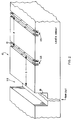
- the specific embodiment shown in Figure 1 aligns a single-mode fiber array having a plurality of fibers to a diode laser array having a plurality of lasers. Alignment is accomplished by use of a micromachined substrate onto which the laser and fiber arrays are attached.
- the micromachined features are designed so that each laser/fiber pair is precisely positioned on the substrate and thereby automatically aligned to each other.
- Fig. 1 illustrates the passive laser/fiber alignment procedure according to the present invention for a four-element laser array chip 10 coupled into a four-fiber array 11.
- Photolithographic techniques such as wet chemical etching are used to fabricate V-grooves (not shown) in a silicon substrate 16 for receiving the fibers of array 11 during the alignment procedure.
- silicon is cited as an example of a substrate material in the embodiment of Fig. 1, other materials may also be used. Silicon provides an excellent substrate for defining micromachined features because of its well established processing technology.
- Three pedestals 12, 13, and 14 fabricated on substrate 16 at predetermined locations serve to position the laser array chip on the substrate.
- the groove pitch is designed to be the same as the separation between the lasers on the array to enable alignment in the y-direction.
- a mating channel shown as the lip extending over pedestal 14 is fabricated into the laser chip.
- the laser chip is mounted epi-side down so that it is in abutting contact with a contact surface of each pedestal.
- the known position of the laser emitting regions with respect to the laser chip array and the location of the pedestals allow positioning of the grooves for locating the fibers in the x, y and z directions at the appropriate angular orientation so that the center line of each laser active region is aligned to the center line of each fiber.
- a metallization 15 pattern is used for electrical access to each element of the laser array.
- the substrate side of the laser would be used as a common contact for all four lasers in the array.
- the laser array chip 10 is positioned in the x and y directions by being pushed up against the three pedestals 12, 13, and 14, where the position of the laser array in the x direction (towards the fibers) is determined by pedestals 12 and 13, while alignment of the center line of the laser active regions to the center of the fiber cores (y direction) is achieved by pedestal 14.
- the position of the laser array in this direction must be controlled to within 1-2 ⁇ m to obtain good optical coupling, especially if single-mode fibers are used where the core diameter is on the order of 9 ⁇ m. Achieving this degree of dimensional control requires that the edge 18 of the laser chip, which abuts pedestal 14, be a fixed distance from the active region of the nearest laser element in the array.
- This edge distance then serves as a reference line in the y-direction for etching of the first fiber-receiving groove.
- the orientation of the V-grooves on the substrate 16 determines the position of the fibers in the x and y directions. Photolithographic processing techniques, rather than conventional scribing or sawing processes, can be used to define the laser array chip edge.
- Figure 2 shows a frontal cross-sectional portion of the laser array structure in Figure 1 fabricated with a deep, vertical-wall mating channel 22 having an edge 18 that is positioned a fixed distance, D, from the emitting region 23 of the first laser 21 in the array.
- a double-channel ridge waveguide laser geometry is shown in Figure 2
- the chip array can be fabricated with other laser structures such as stripe geometry and buried heterostructure lasers.
- Laser bars are cut into arrays by making a saw cut through the mating channel, leaving the vertical edge 18 that is a controlled distance (D) from the laser active region 23.
- D controlled distance
- the substrate is designed so that the center of the V-grooves are located the same distances D+np from the pedestal surface abutting chip edge 18. This provides automatic alignment between the fibers and lasers in the y-direction.
- Alignment in the z direction of a fiber to its corresponding laser in array chip 10 is accomplished by fixing the fiber core and the laser active region at the same height above the surface of the substrate 16.
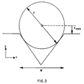
- the position of a fiber in a V-groove, shown in a cross sectional view in Figure 3, is determined by the width, w, of the V-groove and the diameter, d, of the fiber (125 ⁇ m for conventional fibers).
- Placement of the laser emitting region at a controlled height equal to h core above the substrate surface requires a new packaging approach.
- Conventional laser mounting techniques (such as the use of eutectic preforms) provide virtually no control over the thickness of the solder. These soldering techniques will not be adequate to position the laser with the precision required, which is approximately ⁇ 1 ⁇ m.
- the vertical position of each laser active region is controlled by the use of a corrugated laser mounting pattern that is built into the substrate surface.
- the mounting pattern is used in conjunction with solder metallizations having controllable thicknesses.
- Epi-side down mounting of the laser array is preferred since the distance between the laser chip surface and the active region can be accurately controlled during the growth and fabrication processes. An epi-side up approach would not easily provide the necessary control of this dimension since it would require that the substrate thinning process be controlled to within a micron. Epi-side down mounting has the additional benefit of providing reduced thermal impedance.
- FIG. 4(a) A cross sectional view of a portion of the corrugated laser mounting area is shown in Figure 4(a). Only two elements of the laser array are shown (the ones closest to pedestal 14).
- the laser mounting area is fabricated by processing a ridge 41 into the substrate for each laser element, with each ridge being bordered by channels 42 and 43.
- the height of the silicon ridge 41 is fabricated so that it is several microns below the substrate surface 44.
- a controlled thickness of solder 45 (such as In or AuSn) is then deposited surface on the ridge to a height that is slightly above the substrate surface 44. This metallized ridge will electrically contact the laser and is patterned on the substrate 16 in line with the center of the fiber groove (not shown in the Figure 4a).
- Pedestal 14 is located a distance D from the center of the first contact ridge 41 to match the distance shown in Figure 2 from the edge of the mating channel to the first active region of the laser array. The matching of these distances and the equivalence of the groove pitch and active element separation result in laser/fiber alignment in the y direction as previously described.
- the laser array mounting procedure is initiated by positioning the laser array over the laser mounting area using the previously described pedestals so that the chip is in abutting contact with all three pedestals simultaneously. Heat is applied to melt the solder while a downward force is applied on the laser array chip. As the solder melts, the laser array surface will come into contact with the substrate surface and the solder will extrude, resulting in the flow of excess solder 47 and 48 into the channels 42 and 43, respectively. In this manner, a controlled solder film 46 is obtained whose thickness is determined by the height difference between the top of the contact ridge (before solder is deposited) and the substrate surface 44. Containment of the excess solder in the channels also prevents spreading of the solder between the various elements of the laser array.
- the alignment technique of the present invention is expected to provide a low cost approach to the packaging of optoelectronic components. Elimination of time consuming active alignment procedures will reduce the labor costs associated with assembly, while the use of silicon as a packaging medium offers the potential for lower materials cost via the use of batch processing technology.
- multi-mode fibers may be used instead of single-mode fibers.
- the substrate may be etched with other fiber-receiving conduits other than V-grooves so long as the conduits permit the same alignment in the x, y, and z directions as the embodiment of Figure 1.
- mounting surfaces other than the one shown in Figures 4a-b may be fabricated.
- One exemplary mounting area would consist of dielectric platforms fabricated to a known height (h dielectric ) above the substrate surface, with solder ridges being deposited at a height slightly above h dielectric between the dielectric platforms.
- the laser chip is firmly pressed onto this mounting area so that each laser element is soldered to a solder ridge and the chip surface rests on the dielectric platforms.
- h core h laser +h dielectric .
- the pedestals 12 and 13 in Figure 1 are in front of the chip, they may also be located behind the chip. However, the front-positioning is preferable because it offers flexibility in increasing chip size without affecting the axial positioning of the fibers.
Landscapes
- Physics & Mathematics (AREA)
- General Physics & Mathematics (AREA)
- Optics & Photonics (AREA)
- Condensed Matter Physics & Semiconductors (AREA)
- Electromagnetism (AREA)
- Optical Couplings Of Light Guides (AREA)
- Semiconductor Lasers (AREA)
Applications Claiming Priority (2)
| Application Number | Priority Date | Filing Date | Title |
|---|---|---|---|
| US07/551,219 US5077878A (en) | 1990-07-11 | 1990-07-11 | Method and device for passive alignment of diode lasers and optical fibers |
| US551219 | 1990-07-11 |
Publications (3)
| Publication Number | Publication Date |
|---|---|
| EP0466134A2 true EP0466134A2 (de) | 1992-01-15 |
| EP0466134A3 EP0466134A3 (en) | 1992-06-17 |
| EP0466134B1 EP0466134B1 (de) | 2000-05-17 |
Family
ID=24200344
Family Applications (1)
| Application Number | Title | Priority Date | Filing Date |
|---|---|---|---|
| EP91111501A Expired - Lifetime EP0466134B1 (de) | 1990-07-11 | 1991-07-10 | Methode zum passiven Ausrichten von Diodenlaser-Arrays und optischen Fasern |
Country Status (5)
| Country | Link |
|---|---|
| US (1) | US5077878A (de) |
| EP (1) | EP0466134B1 (de) |
| JP (1) | JP3147313B2 (de) |
| CA (1) | CA2046716C (de) |
| DE (1) | DE69132202T2 (de) |
Cited By (12)
| Publication number | Priority date | Publication date | Assignee | Title |
|---|---|---|---|---|
| EP0629888A3 (de) * | 1993-06-18 | 1995-01-18 | Sel Alcatel Ag | |
| EP0638829A1 (de) * | 1993-08-09 | 1995-02-15 | Nippon Telegraph And Telephone Corporation | Optoelektronische Hybridintegrationsplattform, optisches Untermodul, optoelektronische hybridintegrierte Schaltung, und Herstellungsverfahren der Plattform |
| WO1995016217A1 (de) * | 1993-12-10 | 1995-06-15 | Siemens Aktiengesellschaft | Elektrooptisches modul |
| WO1996000918A1 (en) * | 1994-06-29 | 1996-01-11 | British Telecommunications Public Limited Company | Packaged optical device |
| EP0704732A1 (de) * | 1994-09-28 | 1996-04-03 | Ngk Insulators, Ltd. | Integrierter optoelektronischer Verbund und Stecker |
| WO1997022898A1 (en) * | 1995-12-19 | 1997-06-26 | Telefonaktiebolaget Lm Ericsson (Publ) | Waveguide connector |
| EP0823760A3 (de) * | 1996-08-06 | 1998-07-15 | The Furukawa Electric Co., Ltd. | Vielfachhalbleiterlaseranordnung |
| EP0864893A3 (de) * | 1997-03-13 | 1999-09-22 | Nippon Telegraph and Telephone Corporation | Montageplattform, optischer Modul mit dieser Montageplattform, und Verfahren zur Herstellung der Plattform und des Moduls |
| EP0682277B1 (de) * | 1994-05-10 | 1999-11-24 | Radiall | Anordnung zur Verbindung von optischen Fasern und Wellenleitern, die auf einem Substrat angebracht sind |
| EP1018050B1 (de) * | 1995-06-30 | 2001-12-12 | The Whitaker Corporation | Vorrichtung zur ausrichtung eines optoelektronischen bauteils |
| US6343164B1 (en) | 1998-03-06 | 2002-01-29 | Telefonaktiebolaget Lm Ericsson (Publ) | Optoelectric multichip module |
| US8265436B2 (en) | 2010-05-12 | 2012-09-11 | Industrial Technology Research Institute | Bonding system for optical alignment |
Families Citing this family (36)
| Publication number | Priority date | Publication date | Assignee | Title |
|---|---|---|---|---|
| JP2976642B2 (ja) * | 1991-11-07 | 1999-11-10 | 日本電気株式会社 | 光結合回路 |
| US5355386A (en) * | 1992-11-17 | 1994-10-11 | Gte Laboratories Incorporated | Monolithically integrated semiconductor structure and method of fabricating such structure |
| US6090635A (en) * | 1992-11-17 | 2000-07-18 | Gte Laboratories Incorporated | Method for forming a semiconductor device structure having a laser portion |
| US5420953A (en) * | 1994-02-17 | 1995-05-30 | The Whitaker Corporation | Optoelectronic integration of holograms using (110) oriented silicon on (100) oriented silicon waferboard |
| SE503905C2 (sv) * | 1994-03-16 | 1996-09-30 | Ericsson Telefon Ab L M | Förfarande för framställning av en optokomponent samt optokomponent |
| SE513183C2 (sv) * | 1994-03-18 | 2000-07-24 | Ericsson Telefon Ab L M | Förfarande för framställning av en optokomponent samt kapslad optokomponent |
| US5500910A (en) * | 1994-06-30 | 1996-03-19 | The Whitaker Corporation | Passively aligned holographic WDM |
| US5966486A (en) * | 1996-08-29 | 1999-10-12 | The Whitaker Corporation | Tilted notched for passive optical alignment |
| US6327289B1 (en) * | 1997-09-02 | 2001-12-04 | Matsushita Electric Industrial Co., Ltd. | Wavelength-variable semiconductor laser, optical integrated device utilizing the same, and production method thereof |
| US5981975A (en) * | 1998-02-27 | 1999-11-09 | The Whitaker Corporation | On-chip alignment fiducials for surface emitting devices |
| US6085007A (en) * | 1998-02-27 | 2000-07-04 | Jiang; Ching-Long | Passive alignment member for vertical surface emitting/detecting device |
| US6172997B1 (en) | 1998-06-16 | 2001-01-09 | Aculight Corporation | Integrated semiconductor diode laser pumped solid state laser |
| US6216939B1 (en) * | 1998-12-31 | 2001-04-17 | Jds Uniphase Photonics C.V. | Method for making a hermetically sealed package comprising at least one optical fiber feedthrough |
| EP1122567A1 (de) | 2000-02-02 | 2001-08-08 | Corning Incorporated | Passive Ausrichtung unter Verwendung von geneigter Sockelwand |
| US6883978B2 (en) * | 2003-06-26 | 2005-04-26 | Matsushita Electric Industrial Co., Ltd. | Low cost package design for fiber coupled optical component |
| US6959134B2 (en) * | 2003-06-30 | 2005-10-25 | Intel Corporation | Measuring the position of passively aligned optical components |
| US7284913B2 (en) | 2003-07-14 | 2007-10-23 | Matsushita Electric Industrial Co., Ltd. | Integrated fiber attach pad for optical package |
| US7410088B2 (en) * | 2003-09-05 | 2008-08-12 | Matsushita Electric Industrial, Co., Ltd. | Solder preform for low heat stress laser solder attachment |
| US7021838B2 (en) | 2003-12-16 | 2006-04-04 | Matsushita Electric Industrial Co., Ltd. | Optimizing alignment of an optical fiber to an optical output port |
| US7140783B2 (en) * | 2004-02-06 | 2006-11-28 | Matsushita Electric Industrial Co., Ltd. | Diamond 2D scan for aligning an optical fiber to an optical output port |
| US7263260B2 (en) * | 2005-03-14 | 2007-08-28 | Matsushita Electric Industrial Co., Ltd. | Low cost, high precision multi-point optical component attachment |
| US7951583B2 (en) * | 2006-03-10 | 2011-05-31 | Plc Diagnostics, Inc. | Optical scanning system |
| US8675199B2 (en) * | 2006-03-10 | 2014-03-18 | Plc Diagnostics, Inc. | Waveguide-based detection system with scanning light source |
| US8288157B2 (en) | 2007-09-12 | 2012-10-16 | Plc Diagnostics, Inc. | Waveguide-based optical scanning systems |
| US9528939B2 (en) | 2006-03-10 | 2016-12-27 | Indx Lifecare, Inc. | Waveguide-based optical scanning systems |
| US9976192B2 (en) | 2006-03-10 | 2018-05-22 | Ldip, Llc | Waveguide-based detection system with scanning light source |
| US9423397B2 (en) | 2006-03-10 | 2016-08-23 | Indx Lifecare, Inc. | Waveguide-based detection system with scanning light source |
| GB2461026B (en) * | 2008-06-16 | 2011-03-09 | Plc Diagnostics Inc | System and method for nucleic acids sequencing by phased synthesis |
| US7658552B2 (en) * | 2008-06-28 | 2010-02-09 | Kotura, Inc. | Interface between light source and optical component |
| JP5534155B2 (ja) * | 2009-11-13 | 2014-06-25 | 日本電気株式会社 | デバイス、及びデバイス製造方法 |
| US7949211B1 (en) * | 2010-02-26 | 2011-05-24 | Corning Incorporated | Modular active board subassemblies and printed wiring boards comprising the same |
| US10018566B2 (en) | 2014-02-28 | 2018-07-10 | Ldip, Llc | Partially encapsulated waveguide based sensing chips, systems and methods of use |
| US10319693B2 (en) * | 2014-06-16 | 2019-06-11 | Skorpios Technologies, Inc. | Micro-pillar assisted semiconductor bonding |
| US11181479B2 (en) | 2015-02-27 | 2021-11-23 | Ldip, Llc | Waveguide-based detection system with scanning light source |
| US9606308B2 (en) | 2015-02-27 | 2017-03-28 | International Business Machines Corporation | Three dimensional self-alignment of flip chip assembly using solder surface tension during solder reflow |
| DE102018106685B4 (de) | 2018-03-21 | 2026-08-06 | OSRAM Opto Semiconductors Gesellschaft mit beschränkter Haftung | Halbleiterlaser und projektor |
Family Cites Families (7)
| Publication number | Priority date | Publication date | Assignee | Title |
|---|---|---|---|---|
| US3864018A (en) * | 1973-10-18 | 1975-02-04 | Bell Telephone Labor Inc | Method and means for splicing arrays of optical fibers |
| US4079404A (en) * | 1976-12-30 | 1978-03-14 | International Business Machines Corporation | Self-aligning support structure for optical components |
| JPS59134882A (ja) * | 1983-01-21 | 1984-08-02 | Hitachi Ltd | 発光半導体装置の製造方法 |
| JPS60223185A (ja) * | 1984-04-19 | 1985-11-07 | Nec Corp | 半導体レ−ザ−の製造方法 |
| CA1255382A (en) * | 1984-08-10 | 1989-06-06 | Masao Kawachi | Hybrid optical integrated circuit with alignment guides |
| US4930854A (en) * | 1989-03-03 | 1990-06-05 | The United States Of America As Represented By The Secretary Of The Navy | Optical fiber-to-channel waveguide coupler |
| US4966447A (en) * | 1989-04-28 | 1990-10-30 | At&T Bell Laboratories | Integration of free-space planar optical components |
-
1990
- 1990-07-11 US US07/551,219 patent/US5077878A/en not_active Expired - Lifetime
-
1991
- 1991-07-10 EP EP91111501A patent/EP0466134B1/de not_active Expired - Lifetime
- 1991-07-10 JP JP19501591A patent/JP3147313B2/ja not_active Expired - Lifetime
- 1991-07-10 CA CA002046716A patent/CA2046716C/en not_active Expired - Lifetime
- 1991-07-10 DE DE69132202T patent/DE69132202T2/de not_active Expired - Lifetime
Cited By (25)
| Publication number | Priority date | Publication date | Assignee | Title |
|---|---|---|---|---|
| EP0629888A3 (de) * | 1993-06-18 | 1995-01-18 | Sel Alcatel Ag | |
| US5818994A (en) * | 1993-06-18 | 1998-10-06 | Alcatel N.V. | Device for the unadjusted coupling of a number of optical waveguides to a laser array |
| US6164836A (en) * | 1993-08-09 | 2000-12-26 | Yamada; Yasufumi | Opto-electronic hybrid integration platform, optical sub-module, opto-electronic hybrid integration circuit, and process for fabricating platform |
| EP1083450A1 (de) * | 1993-08-09 | 2001-03-14 | Nippon Telegraph And Telephone Corporation | Optoelektronische Hybridintegrationsplattform, optisches Untermodul, optoelektronische hybridintegrierte Schaltung, und Herstellungsverfahren der Plattform |
| US5621837A (en) * | 1993-08-09 | 1997-04-15 | Nippon Telegraph & Telephone Corporation | Opto-electronic hybrid integration platform, optical sub-module, opto-electronic hybrid integration circuit and process for fabricating platform |
| EP0831349A3 (de) * | 1993-08-09 | 1998-04-01 | Nippon Telegraph And Telephone Corporation | Optoelektronische Hybridintegrationsplattform, optisches Untermodul, optoelektronische hybridintegrierte Schaltung, und Herstellungsverfahren der Plattform |
| US6027254A (en) * | 1993-08-09 | 2000-02-22 | Nippon Telegraph And Telephone Corporation | Opto-electronic hybrid integration platform, optical sub-module, opto-electronic hybrid integration circuit, and process for fabricating platform |
| EP0638829A1 (de) * | 1993-08-09 | 1995-02-15 | Nippon Telegraph And Telephone Corporation | Optoelektronische Hybridintegrationsplattform, optisches Untermodul, optoelektronische hybridintegrierte Schaltung, und Herstellungsverfahren der Plattform |
| EP1089101A1 (de) * | 1993-08-09 | 2001-04-04 | Nippon Telegraph And Telephone Corporation | Optoelektronische Hybridintegrationsplattform, optisches Untermodul, optoelektronische hybridintegrierte Schaltung, und Herstellungsverfahren der Plattform |
| WO1995016217A1 (de) * | 1993-12-10 | 1995-06-15 | Siemens Aktiengesellschaft | Elektrooptisches modul |
| US5737466A (en) * | 1993-12-10 | 1998-04-07 | Siemens Aktiengesellschaft | Electro-optical module with simplified adjustment of the electro-optical elements |
| EP0682277B1 (de) * | 1994-05-10 | 1999-11-24 | Radiall | Anordnung zur Verbindung von optischen Fasern und Wellenleitern, die auf einem Substrat angebracht sind |
| WO1996000918A1 (en) * | 1994-06-29 | 1996-01-11 | British Telecommunications Public Limited Company | Packaged optical device |
| US5852696A (en) * | 1994-06-29 | 1998-12-22 | British Telecommunications Public Limited Company | Packaged optical device |
| EP0704732A1 (de) * | 1994-09-28 | 1996-04-03 | Ngk Insulators, Ltd. | Integrierter optoelektronischer Verbund und Stecker |
| EP1143278A3 (de) * | 1994-09-28 | 2002-03-20 | Ngk Insulators, Ltd. | Integrierter optoelektronischer Verbund und Stecker |
| EP1018050B1 (de) * | 1995-06-30 | 2001-12-12 | The Whitaker Corporation | Vorrichtung zur ausrichtung eines optoelektronischen bauteils |
| WO1997022898A1 (en) * | 1995-12-19 | 1997-06-26 | Telefonaktiebolaget Lm Ericsson (Publ) | Waveguide connector |
| US6317964B1 (en) | 1995-12-19 | 2001-11-20 | Telefonaktiebolaget Lm Ericsson (Publ) | Waveguide connector |
| US6034982A (en) * | 1996-08-06 | 2000-03-07 | The Furukawa Electric Co. | Semiconductor laser array |
| EP0823760A3 (de) * | 1996-08-06 | 1998-07-15 | The Furukawa Electric Co., Ltd. | Vielfachhalbleiterlaseranordnung |
| US6222967B1 (en) | 1997-03-13 | 2001-04-24 | Nippon Telegraph And Telephone Corporation | Packaging platform, optical module using the platform, and methods for producing the platform and the module |
| EP0864893A3 (de) * | 1997-03-13 | 1999-09-22 | Nippon Telegraph and Telephone Corporation | Montageplattform, optischer Modul mit dieser Montageplattform, und Verfahren zur Herstellung der Plattform und des Moduls |
| US6343164B1 (en) | 1998-03-06 | 2002-01-29 | Telefonaktiebolaget Lm Ericsson (Publ) | Optoelectric multichip module |
| US8265436B2 (en) | 2010-05-12 | 2012-09-11 | Industrial Technology Research Institute | Bonding system for optical alignment |
Also Published As
| Publication number | Publication date |
|---|---|
| DE69132202D1 (de) | 2000-06-21 |
| DE69132202T2 (de) | 2000-09-28 |
| JPH04254390A (ja) | 1992-09-09 |
| EP0466134A3 (en) | 1992-06-17 |
| EP0466134B1 (de) | 2000-05-17 |
| JP3147313B2 (ja) | 2001-03-19 |
| US5077878A (en) | 1992-01-07 |
| CA2046716A1 (en) | 1992-01-12 |
| CA2046716C (en) | 2003-09-30 |
Similar Documents
| Publication | Publication Date | Title |
|---|---|---|
| EP0466134B1 (de) | Methode zum passiven Ausrichten von Diodenlaser-Arrays und optischen Fasern | |
| US5163108A (en) | Method and device for passive alignment of diode lasers and optical fibers | |
| US5574811A (en) | Method and apparatus for providing optical coupling between optical components | |
| US6404960B1 (en) | Flexible optic connector assembly | |
| EP0898724B1 (de) | Anordnung von einer optischen komponente und einem optischen wellenleiter | |
| JP3730664B2 (ja) | 単結晶材料を使用する受動位置合わせフレーム | |
| US5071213A (en) | Optical coupler and method of making optical coupler | |
| US6517257B2 (en) | Optical transmitter/receiver apparatus, method for fabricating the same and optical semiconductor module | |
| US4802727A (en) | Positioning optical components and waveguides | |
| US6238100B1 (en) | Optical module and a method for fabricating a same | |
| US5721797A (en) | Apparatus and method for mounting a laser to a substrate and aligning the laser with an optical conduit | |
| US6023339A (en) | One-dimensional active alignment of optical or opto-electronic devices on a substrate | |
| US10025045B2 (en) | Optical fiber alignment device | |
| JP2003517630A (ja) | Si基板上の能動光学素子および受動光学素子のハイブリッド集積 | |
| US6236788B1 (en) | Arrangement for aligning optical components | |
| JP3040721B2 (ja) | 光結合モジュール | |
| US5436996A (en) | Waferboard structure | |
| US20040022496A1 (en) | High density fibre coupling | |
| US6907178B2 (en) | Optoelectronic assembly with embedded optical and electrical components | |
| CN1118715C (zh) | 用于连接光纤和光波导的结构 | |
| US6249627B1 (en) | Arrangement for self-aligning optical fibers to an array of surface emitting lasers | |
| EP0887674A2 (de) | Optischer Sender/Empfänger,Verfahren zur Herstellung desselben und optisches Halbleitermodul | |
| US20040247248A1 (en) | Passive alignment between waveguides and optical components | |
| US6445837B1 (en) | Hybrid opto-electronic circuits and method of making | |
| JPH08327859A (ja) | 光半導体装置及びその製造方法 |
Legal Events
| Date | Code | Title | Description |
|---|---|---|---|
| PUAI | Public reference made under article 153(3) epc to a published international application that has entered the european phase |
Free format text: ORIGINAL CODE: 0009012 |
|
| AK | Designated contracting states |
Kind code of ref document: A2 Designated state(s): BE DE FR GB IT NL SE |
|
| PUAL | Search report despatched |
Free format text: ORIGINAL CODE: 0009013 |
|
| AK | Designated contracting states |
Kind code of ref document: A3 Designated state(s): BE DE FR GB IT NL SE |
|
| 17P | Request for examination filed |
Effective date: 19920813 |
|
| 17Q | First examination report despatched |
Effective date: 19940304 |
|
| GRAG | Despatch of communication of intention to grant |
Free format text: ORIGINAL CODE: EPIDOS AGRA |
|
| APAB | Appeal dossier modified |
Free format text: ORIGINAL CODE: EPIDOS NOAPE |
|
| APAB | Appeal dossier modified |
Free format text: ORIGINAL CODE: EPIDOS NOAPE |
|
| APAD | Appeal reference recorded |
Free format text: ORIGINAL CODE: EPIDOS REFNE |
|
| APAB | Appeal dossier modified |
Free format text: ORIGINAL CODE: EPIDOS NOAPE |
|
| GRAG | Despatch of communication of intention to grant |
Free format text: ORIGINAL CODE: EPIDOS AGRA |
|
| GRAH | Despatch of communication of intention to grant a patent |
Free format text: ORIGINAL CODE: EPIDOS IGRA |
|
| GRAH | Despatch of communication of intention to grant a patent |
Free format text: ORIGINAL CODE: EPIDOS IGRA |
|
| GRAA | (expected) grant |
Free format text: ORIGINAL CODE: 0009210 |
|
| AK | Designated contracting states |
Kind code of ref document: B1 Designated state(s): BE DE FR GB IT NL SE |
|
| ITF | It: translation for a ep patent filed | ||
| REF | Corresponds to: |
Ref document number: 69132202 Country of ref document: DE Date of ref document: 20000621 |
|
| ET | Fr: translation filed | ||
| PLBE | No opposition filed within time limit |
Free format text: ORIGINAL CODE: 0009261 |
|
| STAA | Information on the status of an ep patent application or granted ep patent |
Free format text: STATUS: NO OPPOSITION FILED WITHIN TIME LIMIT |
|
| 26N | No opposition filed | ||
| REG | Reference to a national code |
Ref country code: GB Ref legal event code: IF02 |
|
| NLT1 | Nl: modifications of names registered in virtue of documents presented to the patent office pursuant to art. 16 a, paragraph 1 |
Owner name: VERIZON LABORATORIES INC. |
|
| REG | Reference to a national code |
Ref country code: FR Ref legal event code: CD |
|
| APAH | Appeal reference modified |
Free format text: ORIGINAL CODE: EPIDOSCREFNO |
|
| PGFP | Annual fee paid to national office [announced via postgrant information from national office to epo] |
Ref country code: NL Payment date: 20100724 Year of fee payment: 20 |
|
| PGFP | Annual fee paid to national office [announced via postgrant information from national office to epo] |
Ref country code: FR Payment date: 20100805 Year of fee payment: 20 Ref country code: SE Payment date: 20100728 Year of fee payment: 20 Ref country code: IT Payment date: 20100728 Year of fee payment: 20 Ref country code: DE Payment date: 20100728 Year of fee payment: 20 |
|
| PGFP | Annual fee paid to national office [announced via postgrant information from national office to epo] |
Ref country code: GB Payment date: 20100726 Year of fee payment: 20 |
|
| PGFP | Annual fee paid to national office [announced via postgrant information from national office to epo] |
Ref country code: BE Payment date: 20100728 Year of fee payment: 20 |
|
| REG | Reference to a national code |
Ref country code: DE Ref legal event code: R071 Ref document number: 69132202 Country of ref document: DE |
|
| REG | Reference to a national code |
Ref country code: DE Ref legal event code: R071 Ref document number: 69132202 Country of ref document: DE |
|
| REG | Reference to a national code |
Ref country code: NL Ref legal event code: V4 Effective date: 20110710 |
|
| BE20 | Be: patent expired |
Owner name: *GTE LABORATORIES INC. Effective date: 20110710 |
|
| REG | Reference to a national code |
Ref country code: GB Ref legal event code: PE20 Expiry date: 20110709 |
|
| REG | Reference to a national code |
Ref country code: SE Ref legal event code: EUG |
|
| PG25 | Lapsed in a contracting state [announced via postgrant information from national office to epo] |
Ref country code: GB Free format text: LAPSE BECAUSE OF EXPIRATION OF PROTECTION Effective date: 20110709 |
|
| PG25 | Lapsed in a contracting state [announced via postgrant information from national office to epo] |
Ref country code: NL Free format text: LAPSE BECAUSE OF EXPIRATION OF PROTECTION Effective date: 20110710 |
|
| PG25 | Lapsed in a contracting state [announced via postgrant information from national office to epo] |
Ref country code: DE Free format text: LAPSE BECAUSE OF EXPIRATION OF PROTECTION Effective date: 20110711 |