EP0466507A1 - Elément de formation d'images photosensibles - Google Patents
Elément de formation d'images photosensibles Download PDFInfo
- Publication number
- EP0466507A1 EP0466507A1 EP91306355A EP91306355A EP0466507A1 EP 0466507 A1 EP0466507 A1 EP 0466507A1 EP 91306355 A EP91306355 A EP 91306355A EP 91306355 A EP91306355 A EP 91306355A EP 0466507 A1 EP0466507 A1 EP 0466507A1
- Authority
- EP
- European Patent Office
- Prior art keywords
- layer
- reflection
- low
- ground plane
- imaging member
- Prior art date
- Legal status (The legal status is an assumption and is not a legal conclusion. Google has not performed a legal analysis and makes no representation as to the accuracy of the status listed.)
- Withdrawn
Links
Images


Classifications
-
- G—PHYSICS
- G03—PHOTOGRAPHY; CINEMATOGRAPHY; ANALOGOUS TECHNIQUES USING WAVES OTHER THAN OPTICAL WAVES; ELECTROGRAPHY; HOLOGRAPHY
- G03G—ELECTROGRAPHY; ELECTROPHOTOGRAPHY; MAGNETOGRAPHY
- G03G5/00—Recording-members for original recording by exposure, e.g. to light, to heat or to electrons; Manufacture thereof; Selection of materials therefor
- G03G5/14—Inert intermediate or cover layers for charge-receiving layers
- G03G5/142—Inert intermediate layers
- G03G5/144—Inert intermediate layers comprising inorganic material
-
- G—PHYSICS
- G03—PHOTOGRAPHY; CINEMATOGRAPHY; ANALOGOUS TECHNIQUES USING WAVES OTHER THAN OPTICAL WAVES; ELECTROGRAPHY; HOLOGRAPHY
- G03G—ELECTROGRAPHY; ELECTROPHOTOGRAPHY; MAGNETOGRAPHY
- G03G5/00—Recording-members for original recording by exposure, e.g. to light, to heat or to electrons; Manufacture thereof; Selection of materials therefor
- G03G5/10—Bases for charge-receiving or other layers
- G03G5/104—Bases for charge-receiving or other layers comprising inorganic material other than metals, e.g. salts, oxides, carbon
Definitions
- the present invention relates in general to electrophotography and, more specifically, to an electrophotographic imaging member and a process for forming the imaging member.
- Multilayered photoreceptors have found increasing usage in electrophotographic copying machines and printers. These photoreceptors can be characterized as "layered photoreceptors" having at least a partially transparent photosensitive layer overlying a conductive ground plane.
- layered photoreceptors One problem inherent in using these layered photoreceptors becomes manifest when exposing the surface of the photoreceptor to a coherent beam of radiation, typically from a helium-neon or laser diode modulated by an image input signal.
- a coherent beam of radiation typically from a helium-neon or laser diode modulated by an image input signal.
- two dominant reflections of the incident coherent light are produced by the photoreceptor; e.g., a first reflection from the top surface and a second reflection from the top surface of the relatively opaque conductive ground plane.
- FIG. 1 This condition is shown in Figure 1; two rays, 1 and 2 of a coherent beam are shown incident on a layered photoreceptor 6 comprising a charge transport layer 7, charge generator layer 8, and a ground plane 9.
- the two dominant reflections are: from the top surface of layer 7, and from the top surface of ground plane 9.
- rays 1 and 2 can interfere constructively or destructively when they combine to form beam 3.
- the illumination that reaches the optically active charge generator layer 8 is modulated by the varying transmission properties of the transparent charge transport layer 7 and can be represented as a spatially varying illumination level will produce variations in the resulting xerographic image.
- This spatial exposure variation present in the image formed on the photoreceptor becomes manifest in the output copy derived from the exposed photoreceptor.
- Figure 2 shows the areas of spatial exposure variation (at 25x) within a photoreceptor of the type shown in Figure 1 when illuminated by a He-Ne laser with an output wavelength of 633 nm.
- the pattern of light and dark interference fringes look like the grains on a sheet of plywood.
- the term "plywood effect" is generically applied to this problem.
- One method of compensating for the plywood effect known to the prior art is to increase the thickness of and, hence, the absorption of the light by the charge generator layer. For most systems, this leads to unacceptable tradeoffs; for example, for a layered organic photoreceptor, an increase in dark decay characteristics and electrical cyclic instability may occur.
- Another method, disclosed in U.S. Patent 4,618,552 is to use a photoconductive imaging member in which the ground plane, or an opaque conductive layer formed above or below the ground plane, is formed with a rough surface morphology to diffusely reflect the light.
- a still further method disclosed in co-pending European patent application No. 91 304 375.8 is to modify the imaging member by forming the ground plane itself of a low reflecting material.
- a second problem associated with the layered photoreceptor is the possibility of separation (delamination) of one or more of the layers at one of the layered interfaces.
- the plywood effect is significantly reduced by suppressing the reflections from the conductive substrate.
- This is accomplished by coating the ground plane with a low-reflection coating of a material with a selected index of refraction, one preferred material being titanium oxide (T i O2).
- T i O2 titanium oxide
- the present invention provides a photosensitive imaging member comprising at least a transparent photoconductive charge transport layer, overlying a charged generator layer and a conductive ground plane, the ground plane being characterized by being coated with a low-reflection material having a refractive index greater than 2.05.
- Figure 1 shows coherent light incident upon a prior art layered photosensitive medium leading to reflections internal to the medium.
- Figure 2 shows a spatial exposure variation plywood pattern in the exposed photosensitive medium of Figure 1 produced when the spatial variation in the absorption within the photosensitive member occurs due to an interference effect.
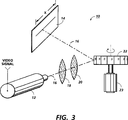
- Figure 3 is a schematic representation of an optical system incorporating a coherent light source to scan a light beam across a photoreceptor.
- Figure 4 is a cross-sectional view of the photoreceptor of Figure 3.
- Figure 5 is a plot of total absorption versus transport layer thickness for photoreceptors incorporating various low-reflection materials.
- Figure 3 shows an imaging system 10 wherein a laser 12 produces a coherent output which is scanned across photoreceptor 14.
- the laser diode is driven so as to provide a modulated light output beam 16.
- Flat field collector and objective lens 18 and 20, respectively, are positioned in the optical path between laser 12 and light beam reflecting scanning device 22.
- device 22 is a multi-faceted mirror polygon driven by motor 23, as shown.
- Flat field collector lens 18 collimates the diverging light beam 16 and field objective lens 20 causes the collected beam to be focused onto photoreceptor 14 after reflection from polygon 22.
- Photoreceptor 14 is a layered photoreceptor shown in partial cross-section in Figure 4.
- photoreceptor 14 is a layered photoreceptor which includes a conductive ground plane 32 formed on a dielectric substrate 34 (typically polyethylene terephthalate (PET)), anti-reflection layer 36, a blocking layer 38, interface layer 40, a charge generating layer 42, and a transparent charge transport layer 44.
- Anti-reflection coating 36 is formed over the ground plane 32.
- a photoreceptor of this type (absent the anti-reflection layer 36) is disclosed in U-S. Patent 4,588,667 to which reference may be made.
- Photoreceptor 14 is subject to both the plywooding effect problem described above as well as the delamination problem, also described above. As will be seen, the thickness of the anti-reflection coating 36 can be selected so as to address either or both problems.
- anti-reflection layer 36 shown in Figure 4, the layer is designed to suppress the reflectivity of the light beams shown in dotted form in Figure 1 from the surface of ground plane 32.
- the layer 36 is formed by means of neon RF sputtering, l-beam evaporation or other coating methods which allow deposition of the layer on the ground plane Layer 36 increases optical transmission through the ground plane thus decreasing its reflectivity. It has been found that the interference fringe contrast decreases as the index of the refraction of layer 36 increases, and that materials with index of refractions of approximately 2.05 or greater are most suitable for use as anti-reflection layers. This is demonstrated by referring to Figure 5 which shows a plot of three different materials used as anti-reflection layer 36.
- the plot shows total absorption plotted against transport layer thickness.
- the coatings shown are of three different materials (M g O, Z r O2, T i O2) as well as a sample plot of absorption in the absence of any anti-reflection coating.
- the thicknesses of each material used as anti-reflection coatings are optimized to produce the lowest reflectivity at the layer 36 surface for a specific wavelength.
- the modulation in the absorption correlates directly to the interference fringe contrast with larger magnitude modulations signifying strong plywood finge-contrast in the final output print. Conversely, a small magnitude modulation-results in weak plywood fringe contrast in the output print.
- T i O2 with an index of 2.5 is a more preferable material than Z r O2 with an index of 2.05 which in turn is preferable to M g O with an index of 1.72.
- a plot of-modulation with no anti-reflection coating at all is shown to be quite close to the M g O plot.
- T i O2 is the material used for layer 36 and if the layer is formed to a thickness of between 20nm and 180nm, the adhesion at the interface of layers 42, 40 is greatly increased.
- the thickness may differ from the optimum thickness stated above.
- the improvement was tested by conducting a series of peel tests which measured reverse peel of adhesion values at the interface of interest. As shown in Table 1, layer T i O2 layers of various thicknesses were applied to a titanium ground plane in a photoreceptor of the type shown in Figure 4. Adhesion values were measured and compared to a control photoreceptor which measured the adhesion without layer 36. As shown, the reverse peel strength was improved by a factor of 7 or 8 times over the control. The optimum thickness of the T i O2 ranges from 20nm to 180nm. In separate tests, electrical parameters of the photoreceptor such as dark decay sensitivity or electrical cyclic stability were not affected.
Landscapes
- Chemical & Material Sciences (AREA)
- Inorganic Chemistry (AREA)
- Physics & Mathematics (AREA)
- General Physics & Mathematics (AREA)
- Photoreceptors In Electrophotography (AREA)
- Laser Beam Printer (AREA)
Applications Claiming Priority (2)
| Application Number | Priority Date | Filing Date | Title |
|---|---|---|---|
| US07/552,200 US5139907A (en) | 1990-07-13 | 1990-07-13 | Photosensitive imaging member |
| US552200 | 1990-07-13 |
Publications (1)
| Publication Number | Publication Date |
|---|---|
| EP0466507A1 true EP0466507A1 (fr) | 1992-01-15 |
Family
ID=24204337
Family Applications (1)
| Application Number | Title | Priority Date | Filing Date |
|---|---|---|---|
| EP91306355A Withdrawn EP0466507A1 (fr) | 1990-07-13 | 1991-07-12 | Elément de formation d'images photosensibles |
Country Status (4)
| Country | Link |
|---|---|
| US (1) | US5139907A (fr) |
| EP (1) | EP0466507A1 (fr) |
| JP (1) | JP3161760B2 (fr) |
| CA (1) | CA2044340C (fr) |
Families Citing this family (11)
| Publication number | Priority date | Publication date | Assignee | Title |
|---|---|---|---|---|
| US5382486A (en) * | 1993-03-29 | 1995-01-17 | Xerox Corporation | Electrostatographic imaging member containing conductive polymer layers |
| US5460911A (en) * | 1994-03-14 | 1995-10-24 | Xerox Corporation | Electrophotographic imaging member free of reflection interference |
| US5525451A (en) * | 1995-05-30 | 1996-06-11 | Xerox Corporation | Photoreceptor fabrication method |
| US5641599A (en) * | 1996-01-11 | 1997-06-24 | Xerox Corporation | Electrophotographic imaging member with improved charge blocking layer |
| US5660961A (en) * | 1996-01-11 | 1997-08-26 | Xerox Corporation | Electrophotographic imaging member having enhanced layer adhesion and freedom from reflection interference |
| US5612157A (en) * | 1996-01-11 | 1997-03-18 | Xerox Corporation | Charge blocking layer for electrophotographic imaging member |
| RU2183030C2 (ru) * | 2000-05-15 | 2002-05-27 | Конструкторско-технологический институт научного приборостроения СО РАН | Считыватель кода с поверхности тел вращения |
| US6557495B2 (en) * | 2000-07-06 | 2003-05-06 | Eileen Lisa Lorenz | Laser pet toy |
| CN100578371C (zh) * | 2005-04-08 | 2010-01-06 | 佳能株式会社 | 电子照相感光构件,以及具有该电子照相感光构件的处理盒和电子照相设备 |
| US8273512B2 (en) | 2009-06-16 | 2012-09-25 | Xerox Corporation | Photoreceptor interfacial layer |
| EP2880991B1 (fr) | 2012-07-31 | 2016-12-07 | Nissin Foods Holdings Co., Ltd. | Nouille instantanée à structure multicouches et son procédé de fabrication |
Citations (5)
| Publication number | Priority date | Publication date | Assignee | Title |
|---|---|---|---|---|
| JPS60170861A (ja) * | 1984-02-16 | 1985-09-04 | Canon Inc | 電子写真感光体 |
| EP0161933A2 (fr) * | 1984-05-15 | 1985-11-21 | Xerox Corporation | Formation d'images électrophotographiques |
| DE3700521A1 (de) * | 1986-01-09 | 1987-07-16 | Ricoh Kk | Elektrophotographisches aufzeichnungsmaterial |
| JPS63131147A (ja) * | 1986-11-21 | 1988-06-03 | Ricoh Co Ltd | 電子写真感光体 |
| JPH01315767A (ja) * | 1988-03-08 | 1989-12-20 | Ricoh Co Ltd | 電子写真感光体 |
Family Cites Families (4)
| Publication number | Priority date | Publication date | Assignee | Title |
|---|---|---|---|---|
| US4361638A (en) * | 1979-10-30 | 1982-11-30 | Fuji Photo Film Co., Ltd. | Electrophotographic element with alpha -Si and C material doped with H and F and process for producing the same |
| US4618552A (en) * | 1984-02-17 | 1986-10-21 | Canon Kabushiki Kaisha | Light receiving member for electrophotography having roughened intermediate layer |
| US4780385A (en) * | 1987-04-21 | 1988-10-25 | Xerox Corporation | Electrophotographic imaging member containing zirconium in base layer |
| US5051328A (en) * | 1990-05-15 | 1991-09-24 | Xerox Corporation | Photosensitive imaging member with a low-reflection ground plane |
-
1990
- 1990-07-13 US US07/552,200 patent/US5139907A/en not_active Expired - Lifetime
-
1991
- 1991-06-11 CA CA002044340A patent/CA2044340C/fr not_active Expired - Fee Related
- 1991-07-06 JP JP16601991A patent/JP3161760B2/ja not_active Expired - Fee Related
- 1991-07-12 EP EP91306355A patent/EP0466507A1/fr not_active Withdrawn
Patent Citations (5)
| Publication number | Priority date | Publication date | Assignee | Title |
|---|---|---|---|---|
| JPS60170861A (ja) * | 1984-02-16 | 1985-09-04 | Canon Inc | 電子写真感光体 |
| EP0161933A2 (fr) * | 1984-05-15 | 1985-11-21 | Xerox Corporation | Formation d'images électrophotographiques |
| DE3700521A1 (de) * | 1986-01-09 | 1987-07-16 | Ricoh Kk | Elektrophotographisches aufzeichnungsmaterial |
| JPS63131147A (ja) * | 1986-11-21 | 1988-06-03 | Ricoh Co Ltd | 電子写真感光体 |
| JPH01315767A (ja) * | 1988-03-08 | 1989-12-20 | Ricoh Co Ltd | 電子写真感光体 |
Non-Patent Citations (3)
| Title |
|---|
| PATENT ABSTRACTS OF JAPAN vol. 10, no. 15 (P-422)(2072) 21 January 1986 & JP-A-60 170 861 ( CANON K.K. ) 4 September 1985 * |
| PATENT ABSTRACTS OF JAPAN vol. 12, no. 388 (P-771)(3235) 17 December 1988 & JP-A-63 131 147 ( RICOH CO. LTD. ) 3 June 1988 * |
| PATENT ABSTRACTS OF JAPAN vol. 14, no. 22 (P-1017)(4065) 7 March 1990 & JP-A-1 315 767 ( RICOH CO. LTD. ) 20 December 1989 * |
Also Published As
| Publication number | Publication date |
|---|---|
| CA2044340C (fr) | 1999-03-23 |
| US5139907A (en) | 1992-08-18 |
| JP3161760B2 (ja) | 2001-04-25 |
| CA2044340A1 (fr) | 1992-01-14 |
| JPH04234051A (ja) | 1992-08-21 |
Similar Documents
| Publication | Publication Date | Title |
|---|---|---|
| EP0457577B1 (fr) | Elément photosensible ayant une base à basse réflection | |
| US5215839A (en) | Method and system for reducing surface reflections from an electrophotographic imaging member | |
| US5089908A (en) | Plywood suppression in ROS systems | |
| EP0465973B1 (fr) | Procédé de fabrication d'éléments de formation d'images photosensibles pour supprimer les effects d'interférences | |
| US4321630A (en) | Linear integrating cavity light collector | |
| US5382486A (en) | Electrostatographic imaging member containing conductive polymer layers | |
| CA2044340C (fr) | Nouvel element d'imagerie photosensible | |
| US5460911A (en) | Electrophotographic imaging member free of reflection interference | |
| KR0164001B1 (ko) | 전자사진 감광 부재, 이를 포함하는 프로세스 카트리지 및 화상 형성 장치 | |
| US5311033A (en) | Layered imaging stack for minimizing interference fringes in an imaging device | |
| JPH0319541B2 (fr) | ||
| JPH04233546A (ja) | 感光性映像部材の化粧板効果抑制装置及び方法 | |
| JPS6129851A (ja) | 電子写真装置 | |
| US5162182A (en) | Photosensitive member for electrophotography with interference control layer | |
| US5525451A (en) | Photoreceptor fabrication method | |
| US4717635A (en) | Electrophotographic recording material | |
| US4592643A (en) | Copying machine having reduced image memory | |
| US5652612A (en) | Apparatus and method for enhancing printing efficiency to reduce artifacts | |
| JPS60147757A (ja) | 感光体に画像露光する装置 | |
| JPH05216264A (ja) | 感光性画像形成体 | |
| JPH0452653A (ja) | 電子写真用感光体の光感度評価方法 | |
| JPH0210948B2 (fr) | ||
| JPH0485543A (ja) | 電子写真用感光体およびその製造方法 | |
| JPS60257453A (ja) | 光受容部材 | |
| JPH0355819B2 (fr) |
Legal Events
| Date | Code | Title | Description |
|---|---|---|---|
| PUAI | Public reference made under article 153(3) epc to a published international application that has entered the european phase |
Free format text: ORIGINAL CODE: 0009012 |
|
| AK | Designated contracting states |
Kind code of ref document: A1 Designated state(s): DE FR GB NL |
|
| STAA | Information on the status of an ep patent application or granted ep patent |
Free format text: STATUS: THE APPLICATION IS DEEMED TO BE WITHDRAWN |
|
| 18D | Application deemed to be withdrawn |
Effective date: 19920716 |