EP0467504A2 - Appareil de traitement de données ayant un circuit anti-blocage - Google Patents
Appareil de traitement de données ayant un circuit anti-blocage Download PDFInfo
- Publication number
- EP0467504A2 EP0467504A2 EP91303440A EP91303440A EP0467504A2 EP 0467504 A2 EP0467504 A2 EP 0467504A2 EP 91303440 A EP91303440 A EP 91303440A EP 91303440 A EP91303440 A EP 91303440A EP 0467504 A2 EP0467504 A2 EP 0467504A2
- Authority
- EP
- European Patent Office
- Prior art keywords
- keyboard
- voltage
- supply
- supply voltage
- reset
- Prior art date
- Legal status (The legal status is an assumption and is not a legal conclusion. Google has not performed a legal analysis and makes no representation as to the accuracy of the status listed.)
- Withdrawn
Links
Images
Classifications
-
- G—PHYSICS
- G06—COMPUTING OR CALCULATING; COUNTING
- G06F—ELECTRIC DIGITAL DATA PROCESSING
- G06F1/00—Details not covered by groups G06F3/00 - G06F13/00 and G06F21/00
- G06F1/24—Resetting means
Definitions
- a circuit interposed between the microcomputer system and its source of AC power monitors the AC line condition and detects when the duration of an outage or other disturbance effectively exceeds a half cycle of AC repetition (0.008 seconds). Upon detecting such, the interposed circuit effectively opens a (triac) switch in the AC delivery path to the system and keeps that switch open for at least 5 to 7 seconds; ostensibly a period long enough to require the system to reset when power is reapplied and yet preclude development of a lock-up condition.
- the present invention is concerned with a species of power related microcomputer system disablement, which may be troublesome in unattended environments and yet is susceptible of a simpler, more efficient and more economical solution than the one presented by Hastings.
- the disablement problem presently of concern occurs when a system microcomputer resets and its keyboard fails to reset.
- the keyboard draws its power from a source of regulated low DC voltage (about 5 volts) in the system and the keyboard intelligence is supposed to be responsive to variations in that voltage to reset whenever the system resets.
- the indication of voltage presented to the keyboard circuits controlling resetting may not correspond to the system voltage indication determining system resetting.
- the system may reset while the keyboard does not.
- keyboard circuits are unable to respond to signals presented by the system, while the latter is rebooting after its reset, and as a result the system -- although not in a lock-up condition itself - - posts an error and places itself in a stopped state preventing it from performing any useful operations. This condition presently is termed a lockout.
- data processing apparatus comprising a data processing system, a power supply for the system and an external information entry device operable to enter information to the processing system and connected to receive a supply voltage from a supply point of the power supply, the system being resettable following an interruption or disturbance of power from the power supply and the entry device being resettable in response to interruption or disturbance of the supply voltage from the supply point, characterised in that an anti-lockout circuit is provided between the supply point and the entry device, the circuit having switch means connected in series between the supply point and the entry device, detecting means powered from the supply point to indicate when the supply voltage drops below a predetermined level at which the system would automatically reset, and switch control means powered from the supply point and which responds to an indication from the detecting means that the supply voltage has fallen below the predetermined level by opening the switch means and thereby interrupting the supply to the entry device, the detecting means including a circuit which holds the switch control means from reclosing the switch means for a period long enough to ensure that the entry device will reset following a drop in the supply
- the anti-lockout circuit can be powered from a low DC voltage system outlet which provides a keyboard DC supply voltage (i.e. by a voltage expected to vary between 0 and 5 volts DC).
- the anti-lockout circuit may employ highly sensitive operational amplifiers and a transistor switch to control a low voltage relay in the path between a system DC voltage outlet and a keyboard.
- the operational amplifiers act to turn off the transistor switch which in turn opens the relay contact.
- the relay contact is then held open until system DC voltage rises above 4.6 volts, and after an additional circuit delay imposed by the operational amplifiers (1 to 2.5 seconds presently) the transistor switch is turned on and the relay contact is closed. This additional delay is selected based on empirical observations of disturbance durations associated with keyboard induced lockouts.
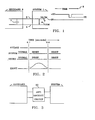
- system 1 and keyboard 2 are ordinarily directly interconnected for transfer of D.C. supply voltage from the system to the keyboard and for bidirectional exchange of information/logic signals.
- D.C supply voltage ports 3 and 4 on the system side extend via respective leads 5 and 6 to corresponding unnumbered voltage ports on the keyboard side.
- Leads 5 and 6 transfer D.C. supply voltage VS/IN to the keyboard; the voltage on lead 5 being referenced to a common potential on lead 6.
- VS/IN is developed from e.g. A. C. utility power in a not-shown power supply unit housed in the system.
- Capacitance 7 schematically represents the capacitive component of the internal impedance of the keyboard.
- the rate at which voltage stored on capacitance 7 decays when VS/IN drops is a function of the impedance present at the keyboard unit.
- the indication of supply voltage presented to keyboard circuits which control resetting action is isolated from the actual supply voltage existing across capacitance 7 and thus subject to different capacitance and charging impedance conditions.
- the indication of supply voltage which determines keyboard reset action may not instantaneously track a drop in actual system supply voltage, and due to this, it is possible to encounter circumstances in which a system will reset and the keyboard does not.
- VS/IN at system port 3 nominally is regulated to stabilise at a level of about + 5 volts relative to common potential at port 4.
- VT is a threshold voltage less than +5 volts at which the system acts to reset and reboot itself. If VS fluctuates but remains above VT, neither the system nor the keyboard is affected and their circuits continue operating normally. If VS/IN varies through VT, not-shown circuits and software in the system operate to reset and reboot the latter. At such times, supply voltage at the keyboard is supposed to track that at port 3 and circuits in the keyboard unit are supposed to operate to reset that unit. However, it is understood that since tracking is not instantaneous due to the capacitance 7, such reset action at the keyboard would vary depending on the actual keyboard design and system power load.
- Figure 2 illustrates the dependence of keyboard operating states relative to the system as a function of durations of AC power disturbances.
- the system power supply has a "holdup feature" allowing it to ride through AC power disturbances lasting less than about 0.1 seconds.
- holdup feature permits the system power supply to reliably hold DC regulated voltage at levels acceptable for continued system operation during AC disturbances shorter than the holdup time.
- both the system and keyboard are unaffected by AC disturbances lasting less than about 0.1 second, and continue normal operation when such disturbances occur; i.e. no reset is performed and no data is lost.
- the system unambiguously resets, and without the present anti-lockout circuit the keyboard may or may not reset depending on whether its capacitively retained DC voltage does or does not decay below VT.
- the alternative offered by the present invention is to prevent such systems from reaching lockout condition by interposing an anti-lockout circuit 20 designed specifically for that purpose.
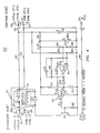
- circuit 20 Details of circuit 20 are shown and described with respect to Fig. 4. In essence, this circuit interrupts continuity from the source 3 of VS/IN on the system side to the keyboard, whenever VS/IN falls below the threshold level VT at which the system would reset, and prevents restoration of continuity in the same path for a period longer than the 0.6 seconds associated with non-zero probability of lockout. This ensures that supply voltage capacitively stored at the keyboard will have decayed below VT before restoration of continuity, thereby ensuring that the keyboard circuits will definitely reset whenever the system does.
- contact 21 in relay K1 and conductor 22 provide a path with interruptible continuity between supply voltage port 23 in the system and a corresponding port 25 in the keyboard unit.
- Conductor 26 provides a continuous conduction path between common port 27 in the system and a corresponding common port 28 in the keyboard.
- Fuse F1 is provided as a safety measure to prevent fire or other hazardous conditions in the event of component failure in the keyboard or in the active circuits in anti-lockout unit 20.
- ports 31-34 in the system and keyboard are used for controllably transferring VS to an additional input device such as a mouse, if present, with the same lockout avoidance purpose as relative to the keyboard.
- Five signal conductors indicated collectively at 36 serve to transfer signals between the keyboard and additional mouse or other input device and the system (2 signal leads and a shield conductor for the keyboard and 2 signal leads and the same shield for the additional mouse device if present).
- the conductors 36, their terminations, and their usage are not relevant to the present discussion, but are shown for completeness.
- Closed and opened states of relay contact 21 are determined by conduction states of transistor Q1.
- Q1 conducts providing sufficient current through coil 40 in K1 to keep contact 21 in closed position, thereby providing continuity between system port 23 and keyboard port 25.
- Diode CR1 prevents build-up of reverse potential on coil 40 when Q1 stops conducting.
- Q1 ceases conducting causing contact 21 to open.
- the conduction state of Q1 is determined by states of operational amplifiers 41 and 42, and associated resistive components R1 through R9 and capacitances C1 through C3. Numbers 5-7 at inputs and outputs of amplifier 41 denote pin numbers (5, 6 are input pin numbers and 7 is the output pin number. Similarly, numbers 1-4 and 8 indicate pin numbers of operational amplifier 42.
- suitable values of the above resistive and capacitive components are:
- Suitable types for relay K1, transistor Q1, Diode CR3 and amplifiers 41 and 42 are:
- supply voltage at 23 is regulated nominally at +5 volts. That voltage is divided by resistors R6 through R8, providing reference regulated voltages of + 3.5 and +2.5 volts at respective junctures of R6 and R7 and R7 and R8. Resulting states of amplifiers 41 and 42 provide a level of conduction through the divider formed by resistors R1 and R2 which is sufficient to maintain Q1 conducting and relay contact 21 closed.
- the 1 to 2.5 seconds delay ensures that any voltage capacitively stored at the keyboard will have decayed at least below the 4.6 volt level at which the keyboard circuits reset.
- +5 volts is reapplied from system port 23 to keyboard port 25 (after the 1 to 2.5 seconds delay)
- operating voltage at the keyboard must rise through +4.6 volts instigating resetting action in the keyboard circuits.
- contact 21 is normally closed when system supply voltage is stable in a range above the threshold level of + 4.6 volts;
- the circuits of Fig. 4 operate to open contact 21, when system outage duration is sufficient to cause a system reset (i.e. sufficient to allow system supply voltage to decay below +4.6 volts), and to keep the contact open long enough (1 to 2.5 seconds) to guarantee decay of any voltage capacitively stored at the keyboard below +4.6 volts; so that (3) upon reclosure of contact 21 the keyboard circuits are subjected to a supply voltage rising through the +4.6 volt level at which they must react by resetting.
- ports 32 and 34 are attached to that device, so that if system VS/IN drops below 4.6 volts application of supply voltage to that device will be interrupted for at least 1 second. This is sufficient to guarantee decay of any capacitively retained voltage at the device below the +4.6 volt level and thereby guarantee that reset circuits in such device will be properly conditioned to perform the requisite reset operation.
- a feature of the invention is that the delay provided by the subject anti-lockout circuit is sufficient to ensure decay of capacitively stored supply voltage indications at the keyboard to a level below the reset voltage threshold of the keyboard. This is important since it ensures that when the relay contact in the subject circuit is reclosed, the keyboard circuitry is presented with a voltage that will then rise smoothly through the reset threshold (at a rate dependent upon the impedance of the keyboard circuits; which would be expected to vary from keyboard to keyboard, especially for keyboards of different make).
- the system power supply is designed to capacitively retain regulated DC outputs for short "holdup” intervals and thereby “ride through” short term AC power disturbances lasting for less than the "holdup” time (typically disturbances lasting for 0.1 seconds or less). Although this does not entirely prevent the above-mentioned keyboard related lockout occurrences, it does serve to protect the system microcomputer from lockup as well as from being reset more frequently. Thus, in contrast to the arrangement of the prior art, wherein reset action is instituted for AC outage times as small as 0.008 seconds, systems having the foregoing holdup feature reset only for much longer disturbances.
- the voltage presented at the DC outlet to the keyboard will not fall below the threshold detected by the present anti-lockout circuit if the disturbance is shorter than the system power holdup time, and therefore the present circuit is effectively reactive only to AC disturbances lasting longer than the system power holdup time.
- the system and keyboard are not as frequently driven to undergo resets as they would be in a system lacking a power holdup feature.
- a feature of the present anti-lockout circuit is that in reacting to the DC level presented at the system to keyboard outlet the keyboard will not reset unless the system does, and in systems with power holdup this means that both the system and its keyboard will not be reset for system AC power disturbances lasting less than the holdup time.
- Lockout also can occur when other input devices are present; e.g. a mouse.
- the time range for such occurrences is generally smaller than that associated with keyboard related lockouts.
- the possibility of lockout occurrence is correspondingly smaller.
- the present anti-lockout circuit can be shared between a keyboard and mouse or other input device so as to positively interrupt the transfer of supply voltage from the system to both devices, and thereby prevent system lockout occurrences relative to both.
- Another feature of the present invention is that it provides an economical means to eliminate lockout problems in existing installations of unattended microcomputer systems and keyboards. Although such problems are correctable by replacement of the existing keyboards with keyboards designed specifically to react more quickly to variations in system DC voltage, the cost of the present circuit is considerably less than that of a keyboard.
Landscapes
- Engineering & Computer Science (AREA)
- Theoretical Computer Science (AREA)
- Physics & Mathematics (AREA)
- General Engineering & Computer Science (AREA)
- General Physics & Mathematics (AREA)
- Input From Keyboards Or The Like (AREA)
- Power Sources (AREA)
Applications Claiming Priority (2)
| Application Number | Priority Date | Filing Date | Title |
|---|---|---|---|
| US553926 | 1990-07-16 | ||
| US07/553,926 US5119264A (en) | 1990-07-16 | 1990-07-16 | Keyboard anti-lockout circuit |
Publications (2)
| Publication Number | Publication Date |
|---|---|
| EP0467504A2 true EP0467504A2 (fr) | 1992-01-22 |
| EP0467504A3 EP0467504A3 (en) | 1993-07-14 |
Family
ID=24211351
Family Applications (1)
| Application Number | Title | Priority Date | Filing Date |
|---|---|---|---|
| EP19910303440 Withdrawn EP0467504A3 (en) | 1990-07-16 | 1991-04-17 | Data processing apparatus having an anti-lockout circuit |
Country Status (4)
| Country | Link |
|---|---|
| US (1) | US5119264A (fr) |
| EP (1) | EP0467504A3 (fr) |
| JP (1) | JP2962372B2 (fr) |
| BR (1) | BR9102965A (fr) |
Cited By (5)
| Publication number | Priority date | Publication date | Assignee | Title |
|---|---|---|---|---|
| EP0896273A1 (fr) * | 1997-08-08 | 1999-02-10 | Siemens Aktiengesellschaft | Circuit pour générer un signal de remise à zéro |
| EP0905736A1 (fr) * | 1997-09-30 | 1999-03-31 | Siemens Aktiengesellschaft | Module de controle programmable |
| EP0895150A3 (fr) * | 1997-08-01 | 2000-01-05 | Pitney Bowes Inc. | Circuit de mise hors tension |
| EP2582012A1 (fr) * | 2011-10-13 | 2013-04-17 | Siemens Aktiengesellschaft | Procédé de fonctionnement d'un appareil électrique |
| EP4167414A1 (fr) * | 2021-10-15 | 2023-04-19 | Open Spiral Investments, SGPS, S.A. | Circuits pour réinitialiser un compteur intelligent et procédés associés |
Families Citing this family (3)
| Publication number | Priority date | Publication date | Assignee | Title |
|---|---|---|---|---|
| US6510064B1 (en) | 1999-03-24 | 2003-01-21 | Dell Products L.P. | Power supply restart circuit |
| JP4565148B2 (ja) * | 2000-05-19 | 2010-10-20 | 豊丸産業株式会社 | 遊技機 |
| JP2008100109A (ja) * | 2008-01-15 | 2008-05-01 | Olympia:Kk | 遊技機及び遊技機における電子回路のリセット方法並びにプログラム |
Family Cites Families (2)
| Publication number | Priority date | Publication date | Assignee | Title |
|---|---|---|---|---|
| JPS6226522A (ja) * | 1985-07-29 | 1987-02-04 | Panafacom Ltd | 停電検出・復電制御方式 |
| US4771356A (en) * | 1987-02-02 | 1988-09-13 | The Toro Company | Method and apparatus for accommodating power disturbances |
-
1990
- 1990-07-16 US US07/553,926 patent/US5119264A/en not_active Expired - Fee Related
-
1991
- 1991-04-17 EP EP19910303440 patent/EP0467504A3/en not_active Withdrawn
- 1991-06-11 JP JP16652091A patent/JP2962372B2/ja not_active Expired - Lifetime
- 1991-07-12 BR BR9102965A patent/BR9102965A/pt unknown
Cited By (5)
| Publication number | Priority date | Publication date | Assignee | Title |
|---|---|---|---|---|
| EP0895150A3 (fr) * | 1997-08-01 | 2000-01-05 | Pitney Bowes Inc. | Circuit de mise hors tension |
| EP0896273A1 (fr) * | 1997-08-08 | 1999-02-10 | Siemens Aktiengesellschaft | Circuit pour générer un signal de remise à zéro |
| EP0905736A1 (fr) * | 1997-09-30 | 1999-03-31 | Siemens Aktiengesellschaft | Module de controle programmable |
| EP2582012A1 (fr) * | 2011-10-13 | 2013-04-17 | Siemens Aktiengesellschaft | Procédé de fonctionnement d'un appareil électrique |
| EP4167414A1 (fr) * | 2021-10-15 | 2023-04-19 | Open Spiral Investments, SGPS, S.A. | Circuits pour réinitialiser un compteur intelligent et procédés associés |
Also Published As
| Publication number | Publication date |
|---|---|
| JP2962372B2 (ja) | 1999-10-12 |
| JPH04271421A (ja) | 1992-09-28 |
| EP0467504A3 (en) | 1993-07-14 |
| BR9102965A (pt) | 1992-02-11 |
| US5119264A (en) | 1992-06-02 |
Similar Documents
| Publication | Publication Date | Title |
|---|---|---|
| EP0426663B1 (fr) | Appareil permettant la commutation definie d'un micro-ordinateur en mode d'attente | |
| US5428252A (en) | Power supply interruption detection and response system for a microcontroller | |
| US4422163A (en) | Power down circuit for data protection in a microprocessor-based system | |
| KR100395131B1 (ko) | 스마트 배터리의 실제 잔류 용량을 표시하기 위한 장치 및방법 | |
| CN110676925B (zh) | Avr旁路继电器焊接检测 | |
| US8060321B2 (en) | System and method for detecting an electrical short across a static switch of an uninterruptible power supply | |
| US6236226B1 (en) | Test method and system for uninterruptible power supply | |
| EP0484745B1 (fr) | Appareil pour la commande d'alimentation d'ordinateur | |
| US5568398A (en) | Electronic operations counter for a voltage regulator controller | |
| EP0467504A2 (fr) | Appareil de traitement de données ayant un circuit anti-blocage | |
| EP0473271B1 (fr) | Alimentation pour appareil de traitement de données | |
| US20140226243A1 (en) | System and method to derive power and trip a circuit breaker from an external device | |
| CA2013296C (fr) | Dispositif et methode d'excitation de memoire | |
| JP2000083325A (ja) | バッテリー状態監視回路、バッテリー装置及び該バッテリー装置を搭載した電子機器 | |
| JP3688474B2 (ja) | バックアップ電源回路及び電子回路装置 | |
| KR940007804B1 (ko) | 컴퓨터 제어시스템을 위한 정전방지 및 파워강하 검출회로 | |
| FI74566C (sv) | Förfarande och anordning i en telefonväxel för eliminering av störning ar. | |
| KR950014627B1 (ko) | 소형전화 교환기내의 중앙처리기 자동 리세트회로 | |
| JPH01256480A (ja) | エレベータの制御装置 | |
| EP0902294B1 (fr) | Circuit de surveillance d'une tension | |
| JP2976345B2 (ja) | 停電検出回路 | |
| JPH11187570A (ja) | 電源装置 | |
| JPS61148554A (ja) | C−mos使用のメモリ装置 | |
| JPH05108503A (ja) | 停電処理方式 | |
| KR910004130Y1 (ko) | 키폰 전화기(kts)의 리셋트 회로 |
Legal Events
| Date | Code | Title | Description |
|---|---|---|---|
| PUAI | Public reference made under article 153(3) epc to a published international application that has entered the european phase |
Free format text: ORIGINAL CODE: 0009012 |
|
| AK | Designated contracting states |
Kind code of ref document: A2 Designated state(s): DE FR GB |
|
| 17P | Request for examination filed |
Effective date: 19920521 |
|
| PUAL | Search report despatched |
Free format text: ORIGINAL CODE: 0009013 |
|
| AK | Designated contracting states |
Kind code of ref document: A3 Designated state(s): DE FR GB |
|
| STAA | Information on the status of an ep patent application or granted ep patent |
Free format text: STATUS: THE APPLICATION HAS BEEN WITHDRAWN |
|
| 18W | Application withdrawn |
Withdrawal date: 19960228 |