EP0467689A2 - Suppresseur de bruit pour le signal de luminance - Google Patents
Suppresseur de bruit pour le signal de luminance Download PDFInfo
- Publication number
- EP0467689A2 EP0467689A2 EP91306570A EP91306570A EP0467689A2 EP 0467689 A2 EP0467689 A2 EP 0467689A2 EP 91306570 A EP91306570 A EP 91306570A EP 91306570 A EP91306570 A EP 91306570A EP 0467689 A2 EP0467689 A2 EP 0467689A2
- Authority
- EP
- European Patent Office
- Prior art keywords
- circuit
- noise
- luminance signal
- high frequency
- video
- Prior art date
- Legal status (The legal status is an assumption and is not a legal conclusion. Google has not performed a legal analysis and makes no representation as to the accuracy of the status listed.)
- Granted
Links
Images


Classifications
-
- H—ELECTRICITY
- H04—ELECTRIC COMMUNICATION TECHNIQUE
- H04N—PICTORIAL COMMUNICATION, e.g. TELEVISION
- H04N5/00—Details of television systems
- H04N5/14—Picture signal circuitry for video frequency region
- H04N5/21—Circuitry for suppressing or minimising disturbance, e.g. moiré or halo
Definitions
- the present invention relates to luminance signal noise suppressor for a television receiver, a video tape recorder, a television tuner and the like, and relates to those able to automatically suppress noise in video signals inputted with much noise in weak electric field receiving regions or zones.
- Fig. 4 shows a block diagram of a conventional luminance signal noise suppressor.
- a noise suppression circuit 21 reduces noise of an input luminance signal a and outputs an output luminance signal f .
- a switch 22 is operated to enable or disable the noise suppression circuit 21. The operation of a luminance signal noise suppressor constructed as described above will be described below.
- the input luminance signal a is inputted to the noise suppression circuit 21, which suppresses or eliminates noise in accordance with a state of the switch 22, or the inputted signal is otherwise outputted as the output luminance signal f .
- the noise suppression circuit not only the noise suppression circuit, but also a contour correction circuit which corrects a contour of a video luminance signal emphasizes noise, thus it is a further object of the present invention to reduce correction quantity of the contour correction circuit or reduce the correction quantity zero automatically in the case of much noise in a weak electric field, thereby suppressing the noise emphasize, and to improve sharpness by increasing the correction quantity of the contour correction circuit in the case of sufficient high frequency components of an input video signal in the case of a strong electric field.
- a luminance signal noise suppressor comprises a high-pass filter circuit, a full-wave rectification circuit, a sample-hold circuit, a noise detection pulse generating circuit, a high frequency component quantity detection circuit, a noise suppression circuit, a contour correction circuit, a fine or detail portion correction circuit, a contour portion correction circuit, a contour portion - detail portion separating circuit, a delay circuit, a first adding circuit and a second adding circuit.
- high frequency components in an input video luminance signal band are extracted by the high-pass filter circuit and applied to full-wave rectification in the full-wave rectification circuit so as to detect the video high frequency components.
- detecting a mean value during a vertical synchronizing period of the detected signals by the sample-hold circuit and holding the detected mean value voltage during an effective video signal period it is shown that there are much noise when the amplitude of the voltage is large.
- the correction quantity of the contour correction circuit or the detail portion correction circuit is increased, thereby making it possible to increase the sharpness of the video signal.
- Fig. 1 is a block diagram showing first embodiment of a luminance signal noise suppressor according to the present invention.
- a high-pass filter circuit 1 extracts high frequency components including noise and detail information signals of an input luminance signal a , and outputs them as a high frequency luminance signal b .
- a full-wave rectification circuit 2 applies full-wave rectification to the high frequency luminance signal b and outputs a rectified high frequency luminance signal c .
- a sample-hole circuit 3 receives an input of noise detection pulse e , smoothes a rectified high frequency luminance signal c holds the smoothed voltage until receiving the input of a next noise detection pulse e and outputs it as a noise detection voltage d .
- a noise detection pulse generating circuit 4 shapes a waveform of a vertical synchronizing signal m so as to exclude or eliminate portions of video signal, character multiplexed signal and the like from the signal m, and outputs it as the detection pulse e .
- a numeral 5 denotes a noise suppression circuit.
- the input luminance signal a is inputted to the high-pass filter circuit 1 and outputted as a high frequency luminance signal b with the high frequency components separated, which is inputted to the full-wave rectification circuit 2.
- the high frequency luminance signal b is applied with full-wave rectification by means of the full-wave rectification circuit 2, thus obtaining the rectified output signal c .
- the rectified signal c is inputted to the sample-hold circuit 3, the rectified signal c is smoothed in the period of the noise detection pulse e which is inputted from the noise detection pulse generating circuit 4, and the smoothed voltage is held at the same time as the pulse disappears, which is outputted as a noise detection voltage d .
- the noise detection voltage d is inputted to a noise suppression circuit 5 which is similar to that in the conventional example, and controls the noise suppression quantity for the input luminance signal a which is inputted to the noise suppression circuit 5.
- an automatic control can be made so that the noise suppression quantity is increased when the noise detection voltage d is high (much noise, and the suppression quantity is reduced or made to zero automatically in a case contrary to the above.
- a noise suppressed output luminance signal f is obtained.
- the noise detection pulse is produced during a vertical synchronizing period free from influences of an effective video signal, thereby enabling an accurate noise quantity detection.
- a noise suppression circuit ON automatically in case a video signal including much noise is inputted in a weak electric field and the like so as to control the suppression quantity automatically by detecting high frequency components of a video signal with a high-pass filter circuit and rectifying these high frequency components in a full-wave rectification circuit, then sample-holding in a sample-hold circuit by a noise detection pulse, and controlling suppression quantity of a noise suppression circuit with a noise detection voltage obtained as the result of the foregoing.
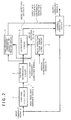
- Fig. 2 is a block diagram of a luminance signal noise suppressor showing a second embodiment of the present invention.
- a numeral 1 denotes a high-pass filter circuit
- 2 denotes a full-wave rectification circuit
- 3 denotes a sample-hold circuit
- 4 denotes a noise detection pulse generating circuit, and these units are the same as those in the first embodiment.
- a contour correction circuit 6 functions to correct the contour of an input luminance signal a so as to increase the sharpness.
- such correction in general, such processing that secondary differential components of an input luminance signal are obtained by using a filter or a delay line and added to an original signal with gain control is employed.
- a high frequency component quantity detection circuit 7 is composed of a smoothing circuit and a switch circuit, and averages voltages of a rectified high frequency luminance signal c during the period when the noise detection pulse is not being inputted and outputs the result as a video high frequency component detection voltage l.
- the process until the noise detection voltage d is obtained is similar to that of the first embodiment.
- the noise is prevented from being emphasized by inputting the noise detection voltage d to the contour correction circuit 6, and suppressing the correction quantity of the contour correction circuit automatically in the same manner as the first embodiment in case of much noise.
- a high frequency component quantity detection circuit 7 is provided, and the rectified high frequency luminance signal c is smoothed during a period when the noise detection pulse e is not being inputted, in a word, a period of an effective video signal, thereby to detect the quantity of high frequency components included in the video luminance signal, and, in case the quantity of high frequency components during the effective video signal period is large and the noise detection voltage d is low (noises are less), the correction quantity of the contour correction circuit is increased on the contrary and contours of detail portions and contour portions of the video signal are emphasized without increasing the noise so much, thus making it possible to increase the sharpness.
- the contour correction circuit As described above, it is possible to suppress the correction quantity of the contour correction circuit and suppress the noise automatically when the noise is much, and the correction quantity is increased automatically when there is no noise and high frequency components of the video signal are much, thereby making it possible to improve the sharpness by applying the noise detection voltage to the contour correction circuit, providing a high frequency component quantity detection circuit, detecting the quantity of the high frequency video signal component during the effective video signal period, and controlling the correction quantity of the contour correction circuit in accordance with the detection result.
- Fig. 3 is a block diagram of a luminance signal noise suppressor showing a third embodiment of the present invention.
- a numeral 1 denotes a high-pass filter circuit
- 2 denotes a full-wave rectification circuit
- 3 denotes a sample-hold circuit
- 4 denotes a noise detection pulse generating circuit, and these units are similar to those in the first embodiment.
- a high frequency component quantity detection circuit 7 is similar to that in the second embodiment. The difference from the construction of the second embodiment exists in that circuits for correcting a contour portion (edge having a comparatively large amplitude of a video signal) and a detail portion (comparatively detail amplitude component of a video signal) are provided separately in place of the contour correction circuit 6.
- a contour portion - detail portion separating circuit 8 applies primary differentiation to a video luminance signal a , divides the variation portion of the video luminance signal a into a detail portion and a contour portion in accordance with the amplitude thereof, and outputs a detail portion signal g and a contour portion signal g based on the result.
- a detail portion correction circuit 9 applies primary differentiation to the detail portion signal g , and outputs a detail portion correction signal i after applying gain control to the amplitude thereof by a noise detection voltage d and a video high frequency component detection voltage l.
- a contour portion correction circuit 10 applies primary differentiation to a contour portion signal h , and outputs the result as a contour portion correction signal j .
- a delay circuit 11 delays the input luminance signal a by the time delay portion due to correction of the contour portion and the detail portion, and outputs a delayed luminance signal n .
- a first adding circuit 12 adds the detail portion correction signal i to the contour portion correction signal j , and outputs a correction signal k .
- a second adding circuit 13 adds the correction signal k to the delayed luminance signal n , and outputs an output luminance signal f .
- the noise detection voltage d is produced in a same manner as the first embodiment.
- a video high frequency component detection voltage l is produced in a same manner as the second embodiment.
- the present embodiment is characterized in that the detail portion containing a noise and the like and the contour portion containing none of them are corrected by means of separate correction circuits, respectively, in accordance with the amplitudes of variation portions of the video signal in place of the contour correction circuit 6.
- the detail portion correction circuit 9 which corrects the detail portion containing a noise and the like with those detected voltages similarly to the second embodiment, the correction quantity of the detail portion correction circuit 9 is reduced automatically in case much noise is contained, and the correction quantity is increased in case no noise and much high frequency components of the video signal are contained, thus making it possible to increase the sharpness.
- circuit 2 indicates a full-wave rectification circuit in above-described embodiments, but similar operation may be performed with a half-wave rectification circuits.
- a high-pass filter circuit a full-wave rectification circuit, a sample-hold circuit, a noise detection pulse generating circuit, a high frequency component quantity detection circuit, a noise suppression circuit, a contour correction circuit, a detail portion correction circuit, a contour portion correction circuit, a contour portion - detail portion separating circuit, a delay circuit, a first adding circuit and a second adding circuit, thus making it possible to automatically suppress the noise in case a weak electric field signal is inputted and also to increase the sharpness of a video luminance signal automatically in a signal containing less noise and much high frequency components in the second and the third embodiments, which is very effectual in practical applications.
Landscapes
- Engineering & Computer Science (AREA)
- Multimedia (AREA)
- Signal Processing (AREA)
- Picture Signal Circuits (AREA)
- Noise Elimination (AREA)
Applications Claiming Priority (2)
| Application Number | Priority Date | Filing Date | Title |
|---|---|---|---|
| JP02190757A JP3094339B2 (ja) | 1990-07-20 | 1990-07-20 | 輝度信号ノイズ抑圧装置 |
| JP190757/90 | 1990-07-20 |
Publications (3)
| Publication Number | Publication Date |
|---|---|
| EP0467689A2 true EP0467689A2 (fr) | 1992-01-22 |
| EP0467689A3 EP0467689A3 (en) | 1992-03-18 |
| EP0467689B1 EP0467689B1 (fr) | 1995-09-20 |
Family
ID=16263228
Family Applications (1)
| Application Number | Title | Priority Date | Filing Date |
|---|---|---|---|
| EP91306570A Expired - Lifetime EP0467689B1 (fr) | 1990-07-20 | 1991-07-18 | Suppresseur de bruit pour le signal de luminance |
Country Status (7)
| Country | Link |
|---|---|
| US (1) | US5200824A (fr) |
| EP (1) | EP0467689B1 (fr) |
| JP (1) | JP3094339B2 (fr) |
| KR (1) | KR950005060B1 (fr) |
| CA (1) | CA2047398C (fr) |
| DE (1) | DE69113154T2 (fr) |
| MY (1) | MY110937A (fr) |
Cited By (2)
| Publication number | Priority date | Publication date | Assignee | Title |
|---|---|---|---|---|
| EP0740463A1 (fr) * | 1995-04-28 | 1996-10-30 | GRUNDIG E.M.V. Elektro-Mechanische Versuchsanstalt Max Grundig GmbH & Co. KG | Dispositif pour l'affichage amélioré de signaux vidéo bruités |
| KR100807003B1 (ko) * | 2000-05-31 | 2008-02-25 | 소니 가부시끼 가이샤 | 신호 처리 장치 및 신호 처리 방법 |
Families Citing this family (13)
| Publication number | Priority date | Publication date | Assignee | Title |
|---|---|---|---|---|
| JP2570565B2 (ja) * | 1993-01-29 | 1997-01-08 | 株式会社栗本鐵工所 | ジョークラッシャーのトッグルブロック固定構造 |
| JP3477871B2 (ja) * | 1994-12-28 | 2003-12-10 | ソニー株式会社 | 映像信号処理装置 |
| JPH09322019A (ja) * | 1996-05-30 | 1997-12-12 | Matsushita Electric Ind Co Ltd | ノイズ抑圧回路 |
| JPH1032834A (ja) * | 1996-07-15 | 1998-02-03 | Nec Corp | 輪郭補償方法ならびに,輪郭補償回路 |
| US6072538A (en) * | 1997-07-22 | 2000-06-06 | Sony Corporation | Digital image enhancement |
| JP2003219208A (ja) | 2002-01-18 | 2003-07-31 | Oki Electric Ind Co Ltd | 映像雑音低減回路 |
| JP4398809B2 (ja) * | 2004-06-30 | 2010-01-13 | 株式会社東芝 | 映像信号処理装置及び映像信号処理方法 |
| JP4626393B2 (ja) * | 2005-05-17 | 2011-02-09 | パナソニック電工株式会社 | 輪郭強調回路 |
| TWI311886B (en) * | 2005-12-05 | 2009-07-01 | Au Optronics Corporatio | Method and video apparatus for auto-compensating weak signal |
| JP4273428B2 (ja) * | 2006-01-31 | 2009-06-03 | ソニー株式会社 | 画像処理装置、画像処理方法、画像処理方法のプログラム及び画像処理方法のプログラムを記録した記録媒体 |
| US7852412B1 (en) * | 2006-02-27 | 2010-12-14 | Nvidia Corporation | Video noise level detection |
| JP4863767B2 (ja) * | 2006-05-22 | 2012-01-25 | ソニー株式会社 | 映像信号処理装置及び画像表示装置 |
| JP6305194B2 (ja) * | 2014-05-08 | 2018-04-04 | キヤノン株式会社 | 画像処理装置、撮像装置および画像処理方法 |
Family Cites Families (4)
| Publication number | Priority date | Publication date | Assignee | Title |
|---|---|---|---|---|
| JPS60154780A (ja) * | 1984-01-25 | 1985-08-14 | Hitachi Ltd | 映像信号処理回路 |
| JPS6251883A (ja) * | 1985-08-30 | 1987-03-06 | Victor Co Of Japan Ltd | ノイズ抑圧回路 |
| JPH01220975A (ja) * | 1988-02-29 | 1989-09-04 | Toshiba Corp | 画質調整回路 |
| JP2532605B2 (ja) * | 1988-09-13 | 1996-09-11 | 松下電器産業株式会社 | 画質補正装置 |
-
1990
- 1990-07-20 JP JP02190757A patent/JP3094339B2/ja not_active Expired - Lifetime
-
1991
- 1991-07-15 US US07/731,152 patent/US5200824A/en not_active Expired - Lifetime
- 1991-07-17 MY MYPI91001283A patent/MY110937A/en unknown
- 1991-07-18 CA CA002047398A patent/CA2047398C/fr not_active Expired - Fee Related
- 1991-07-18 EP EP91306570A patent/EP0467689B1/fr not_active Expired - Lifetime
- 1991-07-18 DE DE69113154T patent/DE69113154T2/de not_active Expired - Fee Related
- 1991-07-19 KR KR1019910012361A patent/KR950005060B1/ko not_active Expired - Fee Related
Cited By (2)
| Publication number | Priority date | Publication date | Assignee | Title |
|---|---|---|---|---|
| EP0740463A1 (fr) * | 1995-04-28 | 1996-10-30 | GRUNDIG E.M.V. Elektro-Mechanische Versuchsanstalt Max Grundig GmbH & Co. KG | Dispositif pour l'affichage amélioré de signaux vidéo bruités |
| KR100807003B1 (ko) * | 2000-05-31 | 2008-02-25 | 소니 가부시끼 가이샤 | 신호 처리 장치 및 신호 처리 방법 |
Also Published As
| Publication number | Publication date |
|---|---|
| CA2047398A1 (fr) | 1992-01-21 |
| MY110937A (en) | 1999-06-30 |
| KR950005060B1 (ko) | 1995-05-17 |
| DE69113154T2 (de) | 1996-05-09 |
| DE69113154D1 (de) | 1995-10-26 |
| EP0467689A3 (en) | 1992-03-18 |
| EP0467689B1 (fr) | 1995-09-20 |
| CA2047398C (fr) | 1998-01-06 |
| JP3094339B2 (ja) | 2000-10-03 |
| JPH0481076A (ja) | 1992-03-13 |
| KR920003743A (ko) | 1992-02-29 |
| US5200824A (en) | 1993-04-06 |
Similar Documents
| Publication | Publication Date | Title |
|---|---|---|
| US5200824A (en) | Luminance signal noise suppressor | |
| JP2517267B2 (ja) | 自動利得制御装置 | |
| US4768094A (en) | Noise suppressing circuit with gain control | |
| US4081836A (en) | Luminance signal processor for providing signal enhancement | |
| US3947631A (en) | Automatic video signal control circuit | |
| EP0986899B1 (fr) | Circuit et procede de correction de contour | |
| US6674486B2 (en) | Signal processor and signal processing method | |
| US4496978A (en) | Noise detecting circuit and television receiver employing the same | |
| EP0142188B1 (fr) | Circuit de correction de pertes de signal pour corriger des signaux vidéo perturbés par des pertes de signal | |
| US4275420A (en) | Television receiver with a ghost detector | |
| EP0059379B1 (fr) | Circuit détecteur de bruit et récepteur de télévision comportant un tel circuit | |
| EP0613310A1 (fr) | Circuit de séparation des signaux de chrominance et de luminance | |
| US4977460A (en) | Video signal reproducing apparatus having setup level elimination | |
| JP2719470B2 (ja) | 色輪郭補正回路 | |
| US5844624A (en) | Television receiver | |
| US5309226A (en) | Means for cancelling ghost signals in response to the reception of a non-standard television video signal | |
| EP0221734A2 (fr) | Détecteur d'interférence ponctuelle | |
| US4651212A (en) | Signal offset circuitry for digital deghosting system | |
| CA1212464A (fr) | Dispositif de detection du son pour la television utilisant une boucle a asservissement de phase pour transposer la frequence | |
| JPH0720251B2 (ja) | 画像合成装置 | |
| JP3228091B2 (ja) | 映像信号の輪郭補正装置 | |
| JPH04243381A (ja) | 映像信号処理回路 | |
| JPS5831668A (ja) | 輪郭補正回路 | |
| JPH0795606A (ja) | 映像色信号の雑音低減装置 | |
| JP2000175077A (ja) | ノイズレベル検出回路 |
Legal Events
| Date | Code | Title | Description |
|---|---|---|---|
| PUAI | Public reference made under article 153(3) epc to a published international application that has entered the european phase |
Free format text: ORIGINAL CODE: 0009012 |
|
| AK | Designated contracting states |
Kind code of ref document: A2 Designated state(s): DE GB |
|
| PUAL | Search report despatched |
Free format text: ORIGINAL CODE: 0009013 |
|
| AK | Designated contracting states |
Kind code of ref document: A3 Designated state(s): DE GB |
|
| 17P | Request for examination filed |
Effective date: 19920422 |
|
| 17Q | First examination report despatched |
Effective date: 19940414 |
|
| GRAA | (expected) grant |
Free format text: ORIGINAL CODE: 0009210 |
|
| AK | Designated contracting states |
Kind code of ref document: B1 Designated state(s): DE GB |
|
| REF | Corresponds to: |
Ref document number: 69113154 Country of ref document: DE Date of ref document: 19951026 |
|
| PLBE | No opposition filed within time limit |
Free format text: ORIGINAL CODE: 0009261 |
|
| STAA | Information on the status of an ep patent application or granted ep patent |
Free format text: STATUS: NO OPPOSITION FILED WITHIN TIME LIMIT |
|
| 26N | No opposition filed | ||
| REG | Reference to a national code |
Ref country code: GB Ref legal event code: IF02 |
|
| PGFP | Annual fee paid to national office [announced via postgrant information from national office to epo] |
Ref country code: DE Payment date: 20050714 Year of fee payment: 15 |
|
| PG25 | Lapsed in a contracting state [announced via postgrant information from national office to epo] |
Ref country code: DE Free format text: LAPSE BECAUSE OF NON-PAYMENT OF DUE FEES Effective date: 20070201 |
|
| PGFP | Annual fee paid to national office [announced via postgrant information from national office to epo] |
Ref country code: GB Payment date: 20100714 Year of fee payment: 20 |
|
| REG | Reference to a national code |
Ref country code: GB Ref legal event code: PE20 Expiry date: 20110717 |
|
| PG25 | Lapsed in a contracting state [announced via postgrant information from national office to epo] |
Ref country code: GB Free format text: LAPSE BECAUSE OF EXPIRATION OF PROTECTION Effective date: 20110717 |