EP0467694B1 - Vorrichtung zur Erzeugung eines dreiphasigen PWM-Signals für Wechselrichter - Google Patents
Vorrichtung zur Erzeugung eines dreiphasigen PWM-Signals für Wechselrichter Download PDFInfo
- Publication number
- EP0467694B1 EP0467694B1 EP91306578A EP91306578A EP0467694B1 EP 0467694 B1 EP0467694 B1 EP 0467694B1 EP 91306578 A EP91306578 A EP 91306578A EP 91306578 A EP91306578 A EP 91306578A EP 0467694 B1 EP0467694 B1 EP 0467694B1
- Authority
- EP
- European Patent Office
- Prior art keywords
- switching
- phase
- command value
- switching pattern
- voltage
- Prior art date
- Legal status (The legal status is an assumption and is not a legal conclusion. Google has not performed a legal analysis and makes no representation as to the accuracy of the status listed.)
- Expired - Lifetime
Links
- 239000013598 vector Substances 0.000 claims description 103
- 230000015572 biosynthetic process Effects 0.000 claims description 6
- 238000010586 diagram Methods 0.000 description 9
- 230000004907 flux Effects 0.000 description 5
- 230000006870 function Effects 0.000 description 2
- 238000006243 chemical reaction Methods 0.000 description 1
- 230000003247 decreasing effect Effects 0.000 description 1
- 238000001514 detection method Methods 0.000 description 1
- 239000006185 dispersion Substances 0.000 description 1
- 230000006698 induction Effects 0.000 description 1
- 238000000034 method Methods 0.000 description 1
- 230000007935 neutral effect Effects 0.000 description 1
- 230000009466 transformation Effects 0.000 description 1
Images


Classifications
-
- H—ELECTRICITY
- H02—GENERATION; CONVERSION OR DISTRIBUTION OF ELECTRIC POWER
- H02M—APPARATUS FOR CONVERSION BETWEEN AC AND AC, BETWEEN AC AND DC, OR BETWEEN DC AND DC, AND FOR USE WITH MAINS OR SIMILAR POWER SUPPLY SYSTEMS; CONVERSION OF DC OR AC INPUT POWER INTO SURGE OUTPUT POWER; CONTROL OR REGULATION THEREOF
- H02M7/00—Conversion of AC power input into DC power output; Conversion of DC power input into AC power output
- H02M7/42—Conversion of DC power input into AC power output without possibility of reversal
- H02M7/44—Conversion of DC power input into AC power output without possibility of reversal by static converters
- H02M7/48—Conversion of DC power input into AC power output without possibility of reversal by static converters using discharge tubes with control electrode or semiconductor devices with control electrode
- H02M7/53—Conversion of DC power input into AC power output without possibility of reversal by static converters using discharge tubes with control electrode or semiconductor devices with control electrode using devices of a triode or transistor type requiring continuous application of a control signal
- H02M7/537—Conversion of DC power input into AC power output without possibility of reversal by static converters using discharge tubes with control electrode or semiconductor devices with control electrode using devices of a triode or transistor type requiring continuous application of a control signal using semiconductor devices only, e.g. single switched pulse inverters
- H02M7/5387—Conversion of DC power input into AC power output without possibility of reversal by static converters using discharge tubes with control electrode or semiconductor devices with control electrode using devices of a triode or transistor type requiring continuous application of a control signal using semiconductor devices only, e.g. single switched pulse inverters in a bridge configuration
- H02M7/53871—Conversion of DC power input into AC power output without possibility of reversal by static converters using discharge tubes with control electrode or semiconductor devices with control electrode using devices of a triode or transistor type requiring continuous application of a control signal using semiconductor devices only, e.g. single switched pulse inverters in a bridge configuration with automatic control of output voltage or current
- H02M7/53875—Conversion of DC power input into AC power output without possibility of reversal by static converters using discharge tubes with control electrode or semiconductor devices with control electrode using devices of a triode or transistor type requiring continuous application of a control signal using semiconductor devices only, e.g. single switched pulse inverters in a bridge configuration with automatic control of output voltage or current with analogue control of three-phase output
-
- H—ELECTRICITY
- H02—GENERATION; CONVERSION OR DISTRIBUTION OF ELECTRIC POWER
- H02M—APPARATUS FOR CONVERSION BETWEEN AC AND AC, BETWEEN AC AND DC, OR BETWEEN DC AND DC, AND FOR USE WITH MAINS OR SIMILAR POWER SUPPLY SYSTEMS; CONVERSION OF DC OR AC INPUT POWER INTO SURGE OUTPUT POWER; CONTROL OR REGULATION THEREOF
- H02M7/00—Conversion of AC power input into DC power output; Conversion of DC power input into AC power output
- H02M7/42—Conversion of DC power input into AC power output without possibility of reversal
- H02M7/44—Conversion of DC power input into AC power output without possibility of reversal by static converters
- H02M7/48—Conversion of DC power input into AC power output without possibility of reversal by static converters using discharge tubes with control electrode or semiconductor devices with control electrode
- H02M7/53—Conversion of DC power input into AC power output without possibility of reversal by static converters using discharge tubes with control electrode or semiconductor devices with control electrode using devices of a triode or transistor type requiring continuous application of a control signal
- H02M7/537—Conversion of DC power input into AC power output without possibility of reversal by static converters using discharge tubes with control electrode or semiconductor devices with control electrode using devices of a triode or transistor type requiring continuous application of a control signal using semiconductor devices only, e.g. single switched pulse inverters
- H02M7/5387—Conversion of DC power input into AC power output without possibility of reversal by static converters using discharge tubes with control electrode or semiconductor devices with control electrode using devices of a triode or transistor type requiring continuous application of a control signal using semiconductor devices only, e.g. single switched pulse inverters in a bridge configuration
- H02M7/53871—Conversion of DC power input into AC power output without possibility of reversal by static converters using discharge tubes with control electrode or semiconductor devices with control electrode using devices of a triode or transistor type requiring continuous application of a control signal using semiconductor devices only, e.g. single switched pulse inverters in a bridge configuration with automatic control of output voltage or current
- H02M7/53873—Conversion of DC power input into AC power output without possibility of reversal by static converters using discharge tubes with control electrode or semiconductor devices with control electrode using devices of a triode or transistor type requiring continuous application of a control signal using semiconductor devices only, e.g. single switched pulse inverters in a bridge configuration with automatic control of output voltage or current with digital control
-
- H—ELECTRICITY
- H02—GENERATION; CONVERSION OR DISTRIBUTION OF ELECTRIC POWER
- H02M—APPARATUS FOR CONVERSION BETWEEN AC AND AC, BETWEEN AC AND DC, OR BETWEEN DC AND DC, AND FOR USE WITH MAINS OR SIMILAR POWER SUPPLY SYSTEMS; CONVERSION OF DC OR AC INPUT POWER INTO SURGE OUTPUT POWER; CONTROL OR REGULATION THEREOF
- H02M7/00—Conversion of AC power input into DC power output; Conversion of DC power input into AC power output
- H02M7/42—Conversion of DC power input into AC power output without possibility of reversal
- H02M7/44—Conversion of DC power input into AC power output without possibility of reversal by static converters
- H02M7/48—Conversion of DC power input into AC power output without possibility of reversal by static converters using discharge tubes with control electrode or semiconductor devices with control electrode
- H02M7/53—Conversion of DC power input into AC power output without possibility of reversal by static converters using discharge tubes with control electrode or semiconductor devices with control electrode using devices of a triode or transistor type requiring continuous application of a control signal
- H02M7/537—Conversion of DC power input into AC power output without possibility of reversal by static converters using discharge tubes with control electrode or semiconductor devices with control electrode using devices of a triode or transistor type requiring continuous application of a control signal using semiconductor devices only, e.g. single switched pulse inverters
- H02M7/5387—Conversion of DC power input into AC power output without possibility of reversal by static converters using discharge tubes with control electrode or semiconductor devices with control electrode using devices of a triode or transistor type requiring continuous application of a control signal using semiconductor devices only, e.g. single switched pulse inverters in a bridge configuration
- H02M7/53871—Conversion of DC power input into AC power output without possibility of reversal by static converters using discharge tubes with control electrode or semiconductor devices with control electrode using devices of a triode or transistor type requiring continuous application of a control signal using semiconductor devices only, e.g. single switched pulse inverters in a bridge configuration with automatic control of output voltage or current
- H02M7/53875—Conversion of DC power input into AC power output without possibility of reversal by static converters using discharge tubes with control electrode or semiconductor devices with control electrode using devices of a triode or transistor type requiring continuous application of a control signal using semiconductor devices only, e.g. single switched pulse inverters in a bridge configuration with automatic control of output voltage or current with analogue control of three-phase output
- H02M7/53876—Conversion of DC power input into AC power output without possibility of reversal by static converters using discharge tubes with control electrode or semiconductor devices with control electrode using devices of a triode or transistor type requiring continuous application of a control signal using semiconductor devices only, e.g. single switched pulse inverters in a bridge configuration with automatic control of output voltage or current with analogue control of three-phase output based on synthesising a desired voltage vector via the selection of appropriate fundamental voltage vectors, and corresponding dwelling times
-
- H—ELECTRICITY
- H02—GENERATION; CONVERSION OR DISTRIBUTION OF ELECTRIC POWER
- H02M—APPARATUS FOR CONVERSION BETWEEN AC AND AC, BETWEEN AC AND DC, OR BETWEEN DC AND DC, AND FOR USE WITH MAINS OR SIMILAR POWER SUPPLY SYSTEMS; CONVERSION OF DC OR AC INPUT POWER INTO SURGE OUTPUT POWER; CONTROL OR REGULATION THEREOF
- H02M7/00—Conversion of AC power input into DC power output; Conversion of DC power input into AC power output
- H02M7/42—Conversion of DC power input into AC power output without possibility of reversal
- H02M7/44—Conversion of DC power input into AC power output without possibility of reversal by static converters
- H02M7/48—Conversion of DC power input into AC power output without possibility of reversal by static converters using discharge tubes with control electrode or semiconductor devices with control electrode
- H02M7/53—Conversion of DC power input into AC power output without possibility of reversal by static converters using discharge tubes with control electrode or semiconductor devices with control electrode using devices of a triode or transistor type requiring continuous application of a control signal
- H02M7/537—Conversion of DC power input into AC power output without possibility of reversal by static converters using discharge tubes with control electrode or semiconductor devices with control electrode using devices of a triode or transistor type requiring continuous application of a control signal using semiconductor devices only, e.g. single switched pulse inverters
- H02M7/539—Conversion of DC power input into AC power output without possibility of reversal by static converters using discharge tubes with control electrode or semiconductor devices with control electrode using devices of a triode or transistor type requiring continuous application of a control signal using semiconductor devices only, e.g. single switched pulse inverters with automatic control of output wave form or frequency
- H02M7/5395—Conversion of DC power input into AC power output without possibility of reversal by static converters using discharge tubes with control electrode or semiconductor devices with control electrode using devices of a triode or transistor type requiring continuous application of a control signal using semiconductor devices only, e.g. single switched pulse inverters with automatic control of output wave form or frequency by pulse-width modulation
Definitions
- This invention relates generally to an inverter device having a plurality of switching elements turned on and off so that a dc voltage is converted to a three-phase ac voltage, and more particularly to a pulse width modulation (PWM) signal generating device for the inverter device provided for controlling on and off operations of each switching element in accordance with a time ratio so that a substantially sinusoidal output voltage is obtained.
- PWM pulse width modulation
- FIG. 7 schematically illustrates an arrangement of an inverter main circuit 10 of the inverter device.
- Each phase voltage is ⁇ V/2 with respect to a virtual neutral point.
- each of the switching elements Sa, Sb, Sc is represented as "1" when the positive switching element 13u, 13v or 13w in each phase is turned on.
- Each of the switching elements Sa, Sb, Sc is represented as "0" when the negative switching elements 13x, 13y or 13z in each phase is turned on. Accordingly, each switching pattern can be represented by substituting "1” or "0” for each of Sa, Sb, Sc. As shown by solid lines in FIG. 8, these switching patterns can be represented as six fundamental voltage vectors out of phase from one another by an electrical angle of 2 ⁇ /6 and two zero vectors (0, 0, 0) and (1, 1, 1).
- FIG. 9 illustrates the three-phase PWM signal generating device for on-off control of the switching elements in the above-described inverter device.
- Phase command value classification means 14 classifies a phase command value ⁇ * into unit regions obtained by dividing an electrical angle of 2 ⁇ /6 into twelve equal parts, for example and calculates a lead angle in the unit region into which the phase command value is classified. The result of classification and the calculated lead angle are produced as 4-bit information.
- Switching pattern determining means 15 is provided for determining the switching patterns corresponding to two kinds of fundamental voltage vectors (voltage space vectors) nearest to the unit region to which the phase command value ⁇ * classified by the phase command value classification means 14 belongs and the switching pattern corresponding to the zero vector.
- the fundamental voltage vectors are out of phase from each other by an electrical angle of ⁇ /3.
- the switching pattern determining means 15 further determines a sequence that these determined switching patterns are delivered to the base terminals of the switching elements 13u-13z.
- two kinds of fundamental voltage vectors of the phases nearest to the phase command value ⁇ * as exemplified in FIG. 8 and the vectors (1, 0, 0), (1, 1, 0) and the zero vector are specified as the switching patterns in the example of FIG. 8.
- One of two kinds of zero vectors (1, 1, 1) and (0, 0, 0) is selected so that the number of the switching operations becomes the smallest in consideration of the previous switching patterns.
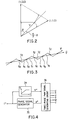
- the voltage space vectors which can be outputted must lie inside a hexagon formed by linking the points of six fundamental voltage vectors in FIG. 8 where the voltage space vectors each having a predetermined magnitude and phase are outputted by controlling the fundamental voltage vectors out of phase from each other by an electrical angle of 2 ⁇ /6 and the zero vector in accordance with the time ratio. Accordingly, the region of the modulation to the sinusoidal waves performed by the above-mentioned control of the fundamental voltage vectors and zero vector is limited to the inside of an inscribed circle of the hexagon. Consequently, polar coordinates can be employed to realize optional voltage space vectors in the limit region and the region of an electrical angle of ⁇ /6 can be described in consideration of the symmetry.
- FIG. 10 shows enlarged fundamental voltage vectors (1, 0, 0), (1, 1, 0) and the zero vector.
- t 1 , t 2 and t 0 are output times of the fundamental voltage vectors (1, 0, 0), (1, 1, 0) and the zero vector and ⁇ is a lead angle of the phase command value ⁇ * in the unit region to which the phase command value ⁇ * belongs.
- Holding time calculating means 16 is provided for obtaining the output times t 1 , t 2 as shown in FIG. 9. More specifically, data of the lead angle ⁇ is supplied to ROM tables 17 and 18 from the phase command classification means 14 so that the value of sin( ⁇ /6+ ⁇ ) corresponding to the supplied lead angle is obtained.
- the holding time t 1 of the switching pattern corresponding to the fundamental voltage vector (1, 0, 0) is obtained by multiplying one control period T SW by the voltage command value V* and further by the value of sin( ⁇ /6- ⁇ ).
- the holding time t 2 of the switching pattern corresponding to the fundamental voltage vector (1, 1, 0) is obtained by multiplying one control period T SW by the voltage command value V* and further by the value of sin( ⁇ /6+ ⁇ ).
- the holding time t 0 of the switching pattern corresponding to the zero vector is obtained by subtracting these holding periods t 1 and t 2 from the one control period T SW .
- One control period refers to a period in which the switching patterns corresponding to the two kinds of fundamental voltage vectors and the zero vector respectively are sequentially produced once.
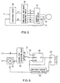
- Timing means 19 comprises a presettable counter 20, a switch 21 and a D-type flip flop 22.
- the presettable counter 20 has a data input terminal DATA to which data of each of the holding times t 0 , t 1 , t 2 is inputted in accordance with the switching of the switch 21.
- the presettable counter 20 also has a clock terminal CK to which clock signals fck are inputted.
- the switch 21 is switched to an output terminal of the holding time corresponding to the switching pattern determined by the switching pattern determining means 15 when timing of each of the holding times supplied to the presettable counter 20 is completed and then, the subsequent holding time data is inputted to the data input terminal DATA.
- the flip flop 22 holds the formation state of the corresponding switching pattern until the timing of each holding time is completed, whereby the switching elements 13u-13z of the inverter device are desirably controlled to be turned on and off.
- FIG. 11 illustrates a locus of a vector ⁇ representative of a magnetic flux induced in a three-phase induction motor M as a three-phase load when an output of the inverter main circuit 10 controlled by the above-described PWM signal generating device is supplied to the motor M.
- Reference symbol ⁇ ' designates a mean locus and figures a circular orbit.
- the magnetic flux vector ⁇ is represented as the time integral of the voltage space vector. Since each fundamental voltage vector has a predetermined value, the direction of the magnetic flux vector ⁇ is the same as that of each fundamental voltage vector and the magnitude of the vector ⁇ is proportional to the holding time of each fundamental voltage vector.
- the output holding times t 1 , t 2 of the switching pattern corresponding to the two fundamental voltage vectors determined by the switching pattern determining means 15 are calculated by the holding time calculating circuit 16.
- the output sequence of the switching patterns is so determined that the zero vector is interposed between longer vectors, that is, the zero vector is positioned at the start or the end of the vector with the longer holding time in one control period T SW .
- the switching pattern corresponding to the fundamental voltage vector with the longer holding time can be determined at the stage of the classification by the phase command value classification means 14.
- FIG.11 shows the case where the phase command value ⁇ * is in the condition shown in FIG. 10.
- the phase command value ⁇ * when t 1 ⁇ t 2 is nearest to the fundamental voltage vector (1,1, 0) where the holding times of the switching patterns corresponding to the fundamental voltage vectors (1, 0, 0), (1, 1, 0) and the zero vector are represented as t 1 , t 2 , t 0 , respectively. Accordingly, the switch 21 is switched so that the sequence of ...t 1 , t 2 , t 0 , t 0 , t 2 , t 1 ... is repeated.
- the switching pattern corresponding to the fundamental voltage vector (1, 0, 0) is held for the time t 1 in the previous control period
- the switching pattern corresponding to the fundamental voltage vector (1, 0, 0) is held for the time t 1 in the following control period and then, the switching pattern corresponding to the fundamental voltage vector (1, 1, 0) is held for the time t 2 and last, the switching pattern corresponding to the zero vector (1, 1, 1) is held for the time t 0 .
- an object of the present invention is to provide a PWM signal generating device for an inverter device wherein the improvement in the degree of approximation of the inverter output voltage waveform to the sinusoidal waveform can be enhanced substantially over the whole PWM control range.
- a three-phase PWM signal generating device for an inverter device comprising an inverter main circuit including six bridge-connected switching elements which can be turned on and off in predetermined patterns so that a dc voltage supplied from an external source is converted to a three-phase ac approximately sinusoidal voltage, the three-phase PWM signal generating device connected to the inverter main circuit for generating switching pattern signals for turning on and off the switching elements in order to provide six kinds of switching patterns corresponding to six fundamental voltage vectors out of phase from one another by an electrical angle of 2 ⁇ /6, respectively, and switching patterns corresponding to a zero vector corresponding to an "on" or “off” state of substantially all the switching elements so that the inverter main circuit generates an approximately sinusoidal output voltage waveform, the three-phase PWM signal generating device comprising phase command value classification means for classifying a phase command value, pertaining to a voltage command value, into one of a plurality of unit regions calculating a lead angle in the one unit region into which the phase command value is classified,
- the switching pattern corresponding to the zero vector wherein the output voltage of the inverter main circuit is decreased substantially to zero is inserted into each of the two fundamental voltage vectors per control period. Consequently, since the on and off control of the switching elements can be performed accurately, the voltage ripple and the torque ripple can be reduced in the range to the maximum PWM controlled voltage.
- Phase command value classification means 30 in the embodiment classifies the supplied phase command value ⁇ * into any one of unit regions obtained by dividing an electrical angle of 2 ⁇ into six equal regions.
- the result of classification by the phase command value classification means 30 is delivered as 3-bit information. Further, the phase command value classification means 30 calculates and delivers a lead angle ⁇ in the classified unit region.
- FIG. 2 is a view similar to FIG. 10 showing a basis of the equation (2).
- Switching pattern determining means 33 is arranged so that switching patterns corresponding to two kinds of fundamental voltage vectors corresponding to the unit region classified by the phase command value classification means 30 and the switching pattern corresponding to the zero vector are delivered in a sequence of (t 1 , t 0 , t 1 ), (t 2 , t 0 , t 2 ), expressing those switching patterns using the respective holding times thereof.
- the switching pattern corresponding to the fundamental voltage vector (1, 0, 0) is held for time t 1 and then, the switching pattern corresponding to the zero vector (0, 0,0) is held for time t 0 .
- the switching pattern corresponding to the fundamental voltage vector (1, 0, 0) is again held for time t 1 and then, the switching pattern corresponding to the fundamental voltage vector (1,1,0) is held for time t 2 .
- the switching pattern corresponding to the zero vector (1, 1, 1) is held for the time t 0 and then, the switching pattern corresponding t 0 the fundamental voltage vector (1,1,0) is again held for the time t 2 .
- the switching pattern corresponding to the zero vector is always inserted once while the switching pattern corresponding to the fundamental voltage vector is delivered twice.
- the switching pattern determining means 33 selects the zero vector (0,0,0) not the zero vector (1,1,1) in the movement from the fundamental voltage vector to the zero vector. This is because only one switching operation is needed when the switching pattern corresponding to the fundamental voltage vector (1,0,0) is transferred to the switching pattern corresponding to the zero vector (0,0,0), whereby the switching loss is reduced to the minimum so that efficient operation is performed.
- the switching pattern corresponding to the zero vector is inserted into each of the switching patterns corresponding to the two kinds of fundamental voltage vectors which form one control cycle. Consequently, the zero vector which is produced at one time in the prior art is dispersed to the two times.
- the approximation of the inverter output voltage waveform can be improved as the result of dispersion of the zero vector.
- the holding times of the zero vectors dispersively produced at the two times are substantially equal to each other or set at substantially the same value t 0 . Consequently, even when the circuit arrangement has a relatively low resolution, a wider control range of the holding time of the zero vector can be ensured, and accordingly, the PWM-controlled maximum voltage can be increased.
- FIG. 4 illustrates a second embodiment wherein the invention is applied to an inverter of the type that the voltage-to-frequency ratio is controlled so as to be constant.
- the reference numeral 36 in FIG. 4 designates a three-phase PWM signal generating device such as shown in FIG. 1.
- a voltage command value V* corresponding to the supplied frequency command value f* is delivered to the three-phase PWM signal generating device 36 by a function generator 34 and the phase command value ⁇ * is delivered to the three-phase PWM signal generating device 36 by a phase signal generator 35 in the same manner as in the first embodiment.
- FIG. 5 illustrates a third embodiment wherein the invention is applied to an inverter of the current follow-up type.
- a detection current value i detected by a current detector 37 provided at the output side of the inverter main circuit 10 having the same configuration as shown in FIG. 18 and a current command value i* are supplied to a conversion circuit 38, these values are converted to the voltage command value V* and the phase command value ⁇ *, both of which command values are supplied to the three-phase PWM signal generating device 36.
- a voltage space vector having an optional voltage and phase can be realized in a time which is twice the control period T SW , the present invention may be applied to high-speed current control when high switching frequency elements are employed.
- FIG. 6 illustrates a fourth embodiment.
- the fourth embodiment differs from the first embodiment in that the holding time calculating means 40 is composed into a function table by the use of a ROM.
- the holding time calculating means 40 is composed into a function table by the use of a ROM.
- the memory capacity required of the ROM is 960 kilobits, which shows that the ROM can be realized by one memory IC of 1 megabit.
Landscapes
- Engineering & Computer Science (AREA)
- Power Engineering (AREA)
- Inverter Devices (AREA)
- Control Of Ac Motors In General (AREA)
Claims (3)
- Dreiphasen-Pulsdauermodulationssignalerzeugungsvorrichtung für eine Wechselrichtervorrichtung mit einer Wechselrichterhauptschaltung (10) mit sechs brückengeschalteten Schaltelementen (13u-13z), die nach vorbestimmten Mustern ein- und ausgeschaltet werden können, so daß eine Gleichspannung, die von einer externen Quelle geliefert wird, in eine annähernd sinusförmige Dreiphasen-Wechselspannung umgewandelt wird, wobei die Dreiphasen-Pulsdauermodulationssignalerzeugungsvorrichtung mit der Wechselrichterhauptschaltung (10) zum Erzeugen von Schaltmustersignalen zum Ein- und Ausschalten der Schaltelemente (13u-13z) verbunden ist, um sechs Arten von Schaltmustern, die sechs Grundspannungsvektoren entsprechen, die jeweils gegeneinander um einen elektrischen Winkel von 2π/6 phasenverschoben sind, und Schaltmuster bereitzustellen, die einem Null-Vektor entsprechen, der einem "Ein"- oder "Aus"-Zustand von im wesentlichen allen Schaltelementen (13u-13z) entspricht, so daß die Wechselrichterhauptschaltung (10) eine annähernd sinusförmige Ausgangsspannungswellenform erzeugt, wobei die Dreiphasen-Pulsdauermodulationssignalerzeugungsvorrichtung aufweist: eine Phasenbefehlswertklassifizierungseinrichtung (30) zum Klassifizieren eines Phasenbefehlswertes (θ*), der sich auf einen Spannungsbefehlswert (V*) bezieht, in einen aus einer Vielzahl von Einheitsbereichen, zum Berechnen eines Voreilwinkels in dem einen Einheitsbereich, in den der Phasenbefehlswert klassifiziert wird, und zum Erzeugen entsprechender Ausgangsinformation, die das Ergebnis der Klassifizierung und den Voreilwinkel darstellt, wobei die Phasenbefehlswertklassifizierungseinrichtung die Vielzahl von Einheitsbereichen ermittelt, indem ein elektrischer Winkel von 2π in eine Vielzahl von gleichen Bereichen geteilt wird, eine Schaltmusterbestimmungseinrichtung (33), die mit der Ausgangsinformation der Phasenbefehlswertklassifizierungseinrichung (30) zum Festlegen der Schaltmuster versorgt wird, die zwei Arten von Grundspannungsvektoren, die dem einen Einheitsbereich entsprechen, in den der Phasenbefehlswert klassifiziert wird, und dem Null-Vektor entsprechen, wobei die Grundspannungsvektoren gegeneinander um einen elektrischen Winkel von π/3 verschoben sind, wobei die Schaltmusterbestimmungseinrichtung (33) ferner eine Ausgangssequenz der festgelegten Schaltmuster festlegt, eine Haltezeitberechnungseinrichtung (16), die mit der Ausgangsinformation der Phasenbefehlswertklassifizierungseinrichung (30) versorgt wird, zum Berechnen einer Haltezeit jedes der Schaltmuster, die den beiden Arten von Grundspannungsvektoren und dem Null-Vektor entsprechen, auf der Grundlage des Voreilwinkels des Phasenbefehlswertes (θ*), der zu dem einen Einheitsbereich gehört, und des gelieferten Spannungsbefehlswertes (V*), und zum Erzeugen von Signalen, die die berechneten Haltezeiten darstellen, und eine Zeitsteuereinrichtung (19), die mit den Signalen versorgt wird, die die berechneten Haltezeiten darstellen, und die mit der Schaltmusterbestimmungseinrichtung (33) verbunden ist, zum Halten eines Bildungszustands jedes festgelegten Schaltmusters während der Haltezeit jedes Schaltmusters, das von der Haltezeitberechnungseinrichtung berechnet wird, dadurch gekennzeichnet, daß die Schaltmusterbestimmungseinrichtung (33) die Schaltmuster, die dem Null-Vektor entsprechen, in jede der beiden Arten von Schaltmustern einmal während der Bildung jedes der beiden Arten von Schaltmustern einfügt und daß die Haltezeiten der Schaltmuster, die den eingefügten beiden Null-Vektoren entsprechen, jeweils im wesentlichen einander gleich sind.
- Dreiphasen-Pulsdauersignalerzeugungsvorrichtung nach Anspruch 1, dadurch gekennzeichnet, daß die Schaltmusterbestimmungseinrichtung (33) zwei Schaltmuster der gleichen Art jeweils vor und nach der Bildung des Schaltmusters bildet, das dem Null-Vektor entspricht.
- Dreiphasen-Pulsdauersignalerzeugungsvorrichtung nach Anspruch 1, dadurch gekennzeichnet, daß die Schaltmusterbestimmungseinrichtung (33) das Schaltmuster bildet, das dem Null-Vektor entspricht, indem eines von drei Schaltelemente, die jedem Schaltmuster entsprechen, in das das Schaltmuster, das dem Null-Vektor entspricht, eingefügt wird, umgekehrt wird.
Priority Applications (1)
| Application Number | Priority Date | Filing Date | Title |
|---|---|---|---|
| EP96100898A EP0713285B1 (de) | 1990-07-20 | 1991-07-19 | Vorrichtung zur Erzeugung eines dreiphasigen PWM-Signals für Wechselrichter |
Applications Claiming Priority (4)
| Application Number | Priority Date | Filing Date | Title |
|---|---|---|---|
| JP02190467A JP3072743B2 (ja) | 1990-07-20 | 1990-07-20 | 三相pwm電圧発生方法 |
| JP190468/90 | 1990-07-20 | ||
| JP2190468A JPH0479770A (ja) | 1990-07-20 | 1990-07-20 | インバータ装置の三相pwm信号発生回路 |
| JP190467/90 | 1990-07-20 |
Related Child Applications (2)
| Application Number | Title | Priority Date | Filing Date |
|---|---|---|---|
| EP96100898A Division EP0713285B1 (de) | 1990-07-20 | 1991-07-19 | Vorrichtung zur Erzeugung eines dreiphasigen PWM-Signals für Wechselrichter |
| EP96100898.4 Division-Into | 1996-01-23 |
Publications (3)
| Publication Number | Publication Date |
|---|---|
| EP0467694A2 EP0467694A2 (de) | 1992-01-22 |
| EP0467694A3 EP0467694A3 (en) | 1992-04-22 |
| EP0467694B1 true EP0467694B1 (de) | 1997-09-17 |
Family
ID=26506103
Family Applications (2)
| Application Number | Title | Priority Date | Filing Date |
|---|---|---|---|
| EP96100898A Expired - Lifetime EP0713285B1 (de) | 1990-07-20 | 1991-07-19 | Vorrichtung zur Erzeugung eines dreiphasigen PWM-Signals für Wechselrichter |
| EP91306578A Expired - Lifetime EP0467694B1 (de) | 1990-07-20 | 1991-07-19 | Vorrichtung zur Erzeugung eines dreiphasigen PWM-Signals für Wechselrichter |
Family Applications Before (1)
| Application Number | Title | Priority Date | Filing Date |
|---|---|---|---|
| EP96100898A Expired - Lifetime EP0713285B1 (de) | 1990-07-20 | 1991-07-19 | Vorrichtung zur Erzeugung eines dreiphasigen PWM-Signals für Wechselrichter |
Country Status (4)
| Country | Link |
|---|---|
| US (1) | US5182701A (de) |
| EP (2) | EP0713285B1 (de) |
| CN (1) | CN1022962C (de) |
| DE (2) | DE69127664T2 (de) |
Cited By (1)
| Publication number | Priority date | Publication date | Assignee | Title |
|---|---|---|---|---|
| US7190601B2 (en) | 2003-08-28 | 2007-03-13 | Vacon Oyj | Pulse-width modulation method for a frequency converter |
Families Citing this family (14)
| Publication number | Priority date | Publication date | Assignee | Title |
|---|---|---|---|---|
| EP0505591B1 (de) * | 1991-03-26 | 1994-07-20 | Siemens Aktiengesellschaft | Verfahren und Schaltungsanordnung zur Regelung eines zweidimensionalen Vektors einer Strecke mittels eines wertediskreten Stellgliedes mit begrenzter Schaltfrequenz |
| US5537308A (en) * | 1993-10-15 | 1996-07-16 | Eaton Corporation | Digital current regulator |
| US5552977A (en) * | 1995-06-20 | 1996-09-03 | Ford Motor Company | Three phase inverter circuit with improved transition from SVPWM to six step operation |
| US5657216A (en) * | 1995-11-13 | 1997-08-12 | Allen-Bradley Company, Inc. | Method and apparatus for linearizing pulse width modulation in overmodulation region |
| US6069808A (en) * | 1997-05-21 | 2000-05-30 | Texas Instruments Incorporated | Symmetrical space vector PWM DC-AC converter controller |
| EP1081842B1 (de) * | 1999-09-01 | 2004-05-26 | Ramachandran Ramarathnam | Motorregler für unterschiedliche Geschwindigkeiten |
| US20060071627A1 (en) * | 2002-03-28 | 2006-04-06 | Ho Eddy Y Y | Motor current reconstruction via DC bus current measurement |
| US7348758B2 (en) * | 2005-10-26 | 2008-03-25 | International Rectifier Corporation | Audible noise reduction for single current shunt platform |
| DE102007035570A1 (de) * | 2007-07-26 | 2009-02-05 | Universität Kassel | Doppelt gespeister Asynchrongenerator und Verfahren zu dessen Betrieb |
| FR2975843B1 (fr) * | 2011-05-23 | 2013-05-17 | Renault Sa | Procede de commande des interrupteurs d'un redresseur de courant connecte a un chargeur embarque. |
| EP2784924B1 (de) | 2011-11-22 | 2018-11-07 | Panasonic Corporation | Ac-wandlerschaltung |
| JP5752275B2 (ja) * | 2012-01-17 | 2015-07-22 | 三菱電機株式会社 | ブラシレスモータ、外部交流電圧源および電動パワーステアリング装置 |
| JP6774622B2 (ja) * | 2016-09-26 | 2020-10-28 | 株式会社ジェイテクト | モータ制御装置 |
| EP4122092A1 (de) * | 2020-03-20 | 2023-01-25 | FRONIUS INTERNATIONAL GmbH | Überwachungseinheit für einen wechselrichter |
Family Cites Families (11)
| Publication number | Priority date | Publication date | Assignee | Title |
|---|---|---|---|---|
| JPH0636676B2 (ja) * | 1985-03-01 | 1994-05-11 | 勲 高橋 | Pwmインバ−タの制御方法 |
| JPH0687676B2 (ja) * | 1985-10-07 | 1994-11-02 | 株式会社豊田中央研究所 | 多相インバ−タの電流制御方法 |
| JPS62118774A (ja) * | 1985-11-18 | 1987-05-30 | Toshiba Corp | インバ−タのパルス幅変調信号発生方式 |
| JP2577738B2 (ja) * | 1987-05-20 | 1997-02-05 | 三菱電機株式会社 | Pwmインバ−タ装置 |
| JPH01152969A (ja) * | 1987-12-07 | 1989-06-15 | Toshiba Corp | インバータ制御装置 |
| JPH0793823B2 (ja) * | 1988-02-01 | 1995-10-09 | 株式会社日立製作所 | 電圧形インバータのpwm制御装置 |
| AU621868B2 (en) * | 1988-04-18 | 1992-03-26 | Daikin Industries, Ltd. | Pulse width modulation control unit of inverter |
| JP2821679B2 (ja) * | 1988-07-19 | 1998-11-05 | 株式会社日立製作所 | Pwmインバータのゲート信号発生方法および装置、pwmインバータ装置 |
| JP2753288B2 (ja) * | 1988-11-30 | 1998-05-18 | 株式会社日立製作所 | Pwmインバータの制御方法およびその制御装置ならびにpwmインバータシステム |
| US4994956A (en) * | 1990-04-25 | 1991-02-19 | Sundstrand Corporation | Enhanced real time control of PWM inverters |
| US4994950A (en) * | 1990-07-31 | 1991-02-19 | Eaton Corporation | Waveform generator for inverter control |
-
1991
- 1991-07-19 DE DE69127664T patent/DE69127664T2/de not_active Expired - Fee Related
- 1991-07-19 EP EP96100898A patent/EP0713285B1/de not_active Expired - Lifetime
- 1991-07-19 US US07/732,837 patent/US5182701A/en not_active Expired - Fee Related
- 1991-07-19 DE DE69130809T patent/DE69130809T2/de not_active Expired - Fee Related
- 1991-07-19 EP EP91306578A patent/EP0467694B1/de not_active Expired - Lifetime
- 1991-07-20 CN CN91105777A patent/CN1022962C/zh not_active Expired - Fee Related
Cited By (1)
| Publication number | Priority date | Publication date | Assignee | Title |
|---|---|---|---|---|
| US7190601B2 (en) | 2003-08-28 | 2007-03-13 | Vacon Oyj | Pulse-width modulation method for a frequency converter |
Also Published As
| Publication number | Publication date |
|---|---|
| DE69127664T2 (de) | 1998-02-12 |
| EP0713285B1 (de) | 1999-01-20 |
| DE69130809D1 (de) | 1999-03-04 |
| EP0713285A2 (de) | 1996-05-22 |
| CN1059239A (zh) | 1992-03-04 |
| EP0467694A3 (en) | 1992-04-22 |
| DE69127664D1 (de) | 1997-10-23 |
| EP0467694A2 (de) | 1992-01-22 |
| EP0713285A3 (de) | 1996-07-24 |
| DE69130809T2 (de) | 1999-09-16 |
| US5182701A (en) | 1993-01-26 |
| CN1022962C (zh) | 1993-12-01 |
Similar Documents
| Publication | Publication Date | Title |
|---|---|---|
| EP0467694B1 (de) | Vorrichtung zur Erzeugung eines dreiphasigen PWM-Signals für Wechselrichter | |
| EP0316006B1 (de) | Pulsbreitenmodulierte Steuereinrichtung | |
| KR100272395B1 (ko) | 다중결합된 전력변환장치 및 그 제어방법 | |
| US4328454A (en) | Apparatus for controlling ac motor | |
| EP0475345B1 (de) | Leistungswechselrichtereinrichtung | |
| KR930022693A (ko) | 3레벨 3상 인버터 장치 | |
| EP0283952A2 (de) | Steuerung für pulsbreitenmodulierten Wechselrichter | |
| US4352154A (en) | Varying two phase voltages in dc to three phase converter | |
| US4349867A (en) | Control apparatus for a cycloconverter | |
| JPH10500278A (ja) | メインズインバータを介して伝送されるべき電力を制御する方法 | |
| US5499177A (en) | Inverter device with a circuit for generating pulse width modulation signals | |
| JPH09182452A (ja) | 3レベルインバータ装置 | |
| JP2582920B2 (ja) | 直流一交流電力変換装置 | |
| JP2635609B2 (ja) | インバータ装置の三相pwm信号発生回路 | |
| GB2238188A (en) | P W M Inverter | |
| GB2171266A (en) | PWM inverter | |
| JP3072743B2 (ja) | 三相pwm電圧発生方法 | |
| US20230396200A1 (en) | Method for operating an electric motor | |
| JPS6159062B2 (de) | ||
| US4688163A (en) | Method for controlling the phase angle of the output current or the output voltage of a frequency converter and apparatus for carrying out the method | |
| KR960016607B1 (ko) | 인버터 장치의 pwm 신호발생회로 | |
| JPH0479770A (ja) | インバータ装置の三相pwm信号発生回路 | |
| EP3745580B1 (de) | Umrichtervorrichtung | |
| KR920002587B1 (ko) | 공진형 인버터의 최적출력전류제어시스템 | |
| JPH06153523A (ja) | Pwm信号生成方法 |
Legal Events
| Date | Code | Title | Description |
|---|---|---|---|
| PUAI | Public reference made under article 153(3) epc to a published international application that has entered the european phase |
Free format text: ORIGINAL CODE: 0009012 |
|
| 17P | Request for examination filed |
Effective date: 19910808 |
|
| AK | Designated contracting states |
Kind code of ref document: A2 Designated state(s): DE FR GB |
|
| PUAL | Search report despatched |
Free format text: ORIGINAL CODE: 0009013 |
|
| AK | Designated contracting states |
Kind code of ref document: A3 Designated state(s): DE FR GB |
|
| 17Q | First examination report despatched |
Effective date: 19950725 |
|
| GRAG | Despatch of communication of intention to grant |
Free format text: ORIGINAL CODE: EPIDOS AGRA |
|
| GRAH | Despatch of communication of intention to grant a patent |
Free format text: ORIGINAL CODE: EPIDOS IGRA |
|
| GRAH | Despatch of communication of intention to grant a patent |
Free format text: ORIGINAL CODE: EPIDOS IGRA |
|
| GRAA | (expected) grant |
Free format text: ORIGINAL CODE: 0009210 |
|
| AK | Designated contracting states |
Kind code of ref document: B1 Designated state(s): DE FR GB |
|
| XX | Miscellaneous (additional remarks) |
Free format text: TEILANMELDUNG 96100898.4 EINGEREICHT AM 23/01/96. |
|
| REF | Corresponds to: |
Ref document number: 69127664 Country of ref document: DE Date of ref document: 19971023 |
|
| ET | Fr: translation filed | ||
| PLBE | No opposition filed within time limit |
Free format text: ORIGINAL CODE: 0009261 |
|
| STAA | Information on the status of an ep patent application or granted ep patent |
Free format text: STATUS: NO OPPOSITION FILED WITHIN TIME LIMIT |
|
| 26N | No opposition filed | ||
| REG | Reference to a national code |
Ref country code: GB Ref legal event code: 746 Effective date: 19981015 |
|
| REG | Reference to a national code |
Ref country code: FR Ref legal event code: D6 |
|
| PGFP | Annual fee paid to national office [announced via postgrant information from national office to epo] |
Ref country code: FR Payment date: 19990709 Year of fee payment: 9 |
|
| PGFP | Annual fee paid to national office [announced via postgrant information from national office to epo] |
Ref country code: GB Payment date: 19990714 Year of fee payment: 9 |
|
| PGFP | Annual fee paid to national office [announced via postgrant information from national office to epo] |
Ref country code: DE Payment date: 19990716 Year of fee payment: 9 |
|
| PG25 | Lapsed in a contracting state [announced via postgrant information from national office to epo] |
Ref country code: GB Free format text: LAPSE BECAUSE OF NON-PAYMENT OF DUE FEES Effective date: 20000719 |
|
| GBPC | Gb: european patent ceased through non-payment of renewal fee |
Effective date: 20000719 |
|
| PG25 | Lapsed in a contracting state [announced via postgrant information from national office to epo] |
Ref country code: FR Free format text: LAPSE BECAUSE OF NON-PAYMENT OF DUE FEES Effective date: 20010330 |
|
| REG | Reference to a national code |
Ref country code: FR Ref legal event code: ST |
|
| PG25 | Lapsed in a contracting state [announced via postgrant information from national office to epo] |
Ref country code: DE Free format text: LAPSE BECAUSE OF NON-PAYMENT OF DUE FEES Effective date: 20010501 |