EP0468341B1 - Dispositif semi-conducteur comprenant plusieurs puces de diodes électro-luminescentes - Google Patents
Dispositif semi-conducteur comprenant plusieurs puces de diodes électro-luminescentes Download PDFInfo
- Publication number
- EP0468341B1 EP0468341B1 EP91111858A EP91111858A EP0468341B1 EP 0468341 B1 EP0468341 B1 EP 0468341B1 EP 91111858 A EP91111858 A EP 91111858A EP 91111858 A EP91111858 A EP 91111858A EP 0468341 B1 EP0468341 B1 EP 0468341B1
- Authority
- EP
- European Patent Office
- Prior art keywords
- lead electrodes
- semiconductor device
- tip portion
- tip portions
- lead
- Prior art date
- Legal status (The legal status is an assumption and is not a legal conclusion. Google has not performed a legal analysis and makes no representation as to the accuracy of the status listed.)
- Expired - Lifetime
Links
Images

Classifications
-
- H—ELECTRICITY
- H10—SEMICONDUCTOR DEVICES; ELECTRIC SOLID-STATE DEVICES NOT OTHERWISE PROVIDED FOR
- H10H—INORGANIC LIGHT-EMITTING SEMICONDUCTOR DEVICES HAVING POTENTIAL BARRIERS
- H10H20/00—Individual inorganic light-emitting semiconductor devices having potential barriers, e.g. light-emitting diodes [LED]
- H10H20/80—Constructional details
- H10H20/85—Packages
- H10H20/857—Interconnections, e.g. lead-frames, bond wires or solder balls
-
- H—ELECTRICITY
- H10—SEMICONDUCTOR DEVICES; ELECTRIC SOLID-STATE DEVICES NOT OTHERWISE PROVIDED FOR
- H10W—GENERIC PACKAGES, INTERCONNECTIONS, CONNECTORS OR OTHER CONSTRUCTIONAL DETAILS OF DEVICES COVERED BY CLASS H10
- H10W90/00—Package configurations
-
- H—ELECTRICITY
- H10—SEMICONDUCTOR DEVICES; ELECTRIC SOLID-STATE DEVICES NOT OTHERWISE PROVIDED FOR
- H10W—GENERIC PACKAGES, INTERCONNECTIONS, CONNECTORS OR OTHER CONSTRUCTIONAL DETAILS OF DEVICES COVERED BY CLASS H10
- H10W90/00—Package configurations
- H10W90/701—Package configurations characterised by the relative positions of pads or connectors relative to package parts
- H10W90/751—Package configurations characterised by the relative positions of pads or connectors relative to package parts of bond wires
- H10W90/756—Package configurations characterised by the relative positions of pads or connectors relative to package parts of bond wires between a chip and a stacked lead frame, conducting package substrate or heat sink
Definitions
- the present invention relates to a remodeled version of an optical semiconductor device in which a plurality of semiconductor elements are arranged on the end surface of the tip portion of a lead electrode, and a connecting area for a bonding wire, i.e. a bonding area, is formed on the end surface of the tip portion of each of other lead electrodes.
- Figs. 1 and 2 show conventional LED lamps, which are a type of optical semiconductor device in which a plurality of semiconductor elements are arranged on the end surface of the tip portion of a lead electrode, and a bonding area is formed on the end surface of the tip portion of each of other lead electrodes.
- the LED lamp shown in Fig. 1 includes three lead electrodes.
- One is a mount-use lead electrode 501 on the end surface of the tip portion of which a plurality of semiconductor elements, i.e. LED chips, are arranged, and the other two are bond-use lead electrodes 502 on the end surface of the tip portion of each of which a bonding area is formed.
- the mount-use lead electrode 501 is provided between the bond-use lead electrodes 502.
- Two LED chips 503 are arranged on the end surface of the tip portion of the mount-use lead electrode 501. Each of the LED chips 503 is connected to each of the bond-use lead electrodes 504 via a bonding wire 504.
- the bond-use lead electrodes 502 are arranged so that they locate both sides of the mount-use lead electrode at the angle of 180° with respect to each other. With this structure, the bonding wires 504 are not contact with each other, and the two LED chips 503 are separately operated.
- the LED lamp shown in Fig. 2 includes four lead electrodes.
- One is a mount-use lead electrode 501 on the end surface of the tip portion of which a plurality of LED chips are arranged, and the other three are bond-use lead electrodes 502 on the end surface of the tip portion of each of which a bonding area is formed.
- Three LED chips are arranged on the end surface of the tip portion of the mount-use lead electrode 501, and each of the LED chips 503 is connected to each of the bond-use lead electrodes 502 via a bonding wire 504.
- the three bond-use lead electrodes 502 of this LED lamp are arranged so that the end surfaces of the tip portions thereof make a straight line. With this structure, the bonding wires 504 locate inevitably very close to each other, and sometimes come cross with each other.
- JP-A-59-159577 describes an optical semiconductor device having three leads which are arranged in an almost straight line.
- JP-A-61-139079 describes an optical semiconductor device having three conductors inserted and fastened to a resin base in such a manner that one end surfaces of the leads shape approximately the same surface, without forming a straight line.
- EP-A-0 198 621 describes a semiconductor device comprising a first lead electrode on which a plurality of semiconductor elements are arranged, a plurality of second lead electrodes each having a tip portion located close to said first lead electrode, and bonding wires for electrically connecting said semiconductor elements to the tip portions of said second lead electrodes whereby said second lead electrodes are arranged such that the end surfaces of the tip ends thereof are not arranged in a straight line.
- An optical semiconductor device comprises a first lead electrode having a tip portion on an end surface of the tip portion a plurality of semiconductor elements being arranged, a plurality of second lead electrodes each having a tip portion located close to the tip portion of the first lead electrode, bonding wires for electrically connecting the semiconductor elements to the tip portions of the second lead electrodes, and a mold resin for covering at least the tip portions of said first and second lead electrodes, said second lead electrodes being arranged such that the end surfaces of the tip ends thereof are not arranged in a straight line.
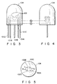
- Figs. 3, 4, and 5 show an LED lamp according to an embodiment of the present invention, and are front, side, and top views of the LED lamp, respectively.
- the LED lamp includes five lead electrodes 101A-101E. Of all the lead electrodes, one located at the center is a mount-use lead electrode 101E on the end surface of the tip portion of which four LED chips 102A-102D are arranged. The other four lead electrodes are bond-use lead electrodes 101A-101D on the end surface of the tip portion of each of which a connecting portion for a bonding wire is formed. The LED chips 102A-102D are connected to the bond-use lead electrodes 101A-101D, respectively, via bonding wires 103. The proximal end section of the lead electrodes 101A-101E group is sealed by a mold resin 104.
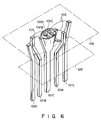
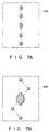
- the mount-use lead electrode 101E and the bond-use lead electrodes 101A-101E constitute, for example, a lead frame. Therefore, as can be seen in Figs. 6 and 7, the lead electrodes 101A-101E are aligned in a plane parallel to the end surfaces of the tip portions, for example, the plane denoted by reference numeral 105 in each of Figs. 6 and 7A.
- the LED lamp of the present invention is characterized in that, of the planes parallel with the end surfaces of the tip portion, there are some on which a plurality of lead electrodes are not aligned.
- the lead electrodes 101A-101E are not aligned at least in the parallel planes located near the tip portion, as of the planes denoted by numeral reference 106 in Figs. 6 and 7.
- the bond-use lead electrodes 101A-101D can be connected to the LED chips 102A-102D without the bonding wires 103 being brought into contact with each other.
- Such an LED lamp can be manufactured by bending bond-use lead electrodes 102 which are next to the mount-use lead electrode 101E at bending points A and B located in the mold resin 104, as can be seen in Figs. 3 and 4 under the condition that the end surface of the tip portion of each of the bond-use lead electrodes 101A-101D becomes parallel with that of the mount-use lead electrode 101E (note that the end surface of the mount-use lead electrode 101E has a plate-like shape, on which the LED chips 102A-102D are arranged).
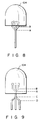
- Fig. 8 shows an LED lamp according to another embodiment of the present invention.
- This LED lamp includes bond-use lead electrodes 101A and 101B which are bent at bending points A and B both located outside a mold resin 104.
- Fig. 9 shows an LED lamp according to another embodiment of the present invention.
- This LED lamp is of a type wherein section of lead electrodes located outside a mold resin 104, i.e. outer leads, are not aligned on a plane which is parallel to the end surface of the tip portion of each of the lead electrodes.
- Such an LED lamp can be manufactured, for example, by bending lead electrodes 101A and 101B at bending points C and D by a lead forming method. Thus, an adjustment of pitch of the lead electrodes 101A-101E can be easily performed.
- the tip portions of the bond-use lead electrodes 101A-101D can be two-dimensionally arranged. Therefore, even if three or more LED chips are mounted on the mount-use lead electrode, large loops as well as crossings of bonding wires can be avoided. Thus, the bonding process can be easily performed.
Landscapes
- Led Device Packages (AREA)
Claims (4)
- Dispositif semiconducteur optique, comportantune première électrode conductrice (101E) possédant une partie d'extrémité, sur une surface terminale de laquelle sont disposés une pluralité d'éléments semiconducteurs (102A à 102D);au moins trois secondes électrodes conductrices (101A à 101D) possédant chacune une partie d'extrémité adjacente à la partie d'extrémité de ladite première électrode conductrice (101E), les surfaces terminales des parties d'extrémité desdites premières et secondes électrodes conductrices (101E, 101A à 101D) étant tournées dans une direction;des fils de connexion (103) reliant électriquement lesdits éléments semiconducteurs (102A à 102D) aux parties d'extrémité desdites secondes électrodes conductrices (101A à 101D); etune résine de moulage (104) recouvrant au moins les parties d'extrémité desdites premières et secondes électrodes conductrices (101E, 101A à 101D);lesdites premières et secondes électrodes conductrices (101E, 101A à 101D) étant formées de manière à former une ligne droite dans au moins un plan (105) parallèle aux parties d'extrémité desdites premières et secondes électrodes conductrices (101E, 101A à 101D); mais les centres des parties d'extrémité desdites secondes électrodes conductrices (101A à 101D) n'étant pas disposés de façon rectiligne.
- Dispositif semiconducteur optique selon la revendication 1, dans lequel lesdites premières et secondes électrodes conductrices (101E, 101A à 101D) comportent chacune des parties qui sont respectivement situées à l'extérieur de ladite résine de moulage (104) et forment une ligne droite dans au moins un plan (105) parallèle aux parties d'extrémité desdites premières et secondes électrodes conductrices (101E, 101A à 101D).
- Dispositif semiconducteur optique selon la revendication 1, dans lequel lesdites premières et secondes électrodes conductrices (101E, 101A à 101D) comportent chacune des parties qui sont respectivement situées à l'extérieur de ladite résine de moulage (104) et forment une ligne non rectiligne dans au moins un plan parallèle aux parties d'extrémité desdites premières et secondes électrodes conductrices (101E, 101A à 101D).
- Dispositif semiconducteur optique selon la revendication 1, dans lequel lesdites premières et secondes électrodes conductrices (101E, 101A à 101D) comportent chacune des parties qui sont respectivement situées à l'intérieur de ladite résine de moulage (104) et forment une ligne non rectiligne dans au moins un plan parallèle aux parties d'extrémité desdites premières et secondes électrodes conductrices (101E, 101A à 101D).
Applications Claiming Priority (2)
| Application Number | Priority Date | Filing Date | Title |
|---|---|---|---|
| JP2195917A JP2535651B2 (ja) | 1990-07-24 | 1990-07-24 | 半導体装置 |
| JP195917/90 | 1990-07-24 |
Publications (2)
| Publication Number | Publication Date |
|---|---|
| EP0468341A1 EP0468341A1 (fr) | 1992-01-29 |
| EP0468341B1 true EP0468341B1 (fr) | 1996-04-10 |
Family
ID=16349134
Family Applications (1)
| Application Number | Title | Priority Date | Filing Date |
|---|---|---|---|
| EP91111858A Expired - Lifetime EP0468341B1 (fr) | 1990-07-24 | 1991-07-16 | Dispositif semi-conducteur comprenant plusieurs puces de diodes électro-luminescentes |
Country Status (5)
| Country | Link |
|---|---|
| US (1) | US5218233A (fr) |
| EP (1) | EP0468341B1 (fr) |
| JP (1) | JP2535651B2 (fr) |
| KR (1) | KR940003744B1 (fr) |
| DE (1) | DE69118602T2 (fr) |
Cited By (1)
| Publication number | Priority date | Publication date | Assignee | Title |
|---|---|---|---|---|
| DE10261365B4 (de) * | 2002-12-30 | 2006-09-28 | Osram Opto Semiconductors Gmbh | Optoelektronisches Bauelement mit einer Mehrzahl von strahlungsemittierenden Halbleiterchips |
Families Citing this family (42)
| Publication number | Priority date | Publication date | Assignee | Title |
|---|---|---|---|---|
| JPH0492659U (fr) * | 1990-12-27 | 1992-08-12 | ||
| JP3096824B2 (ja) * | 1992-04-17 | 2000-10-10 | ローム株式会社 | Led製造用フレームおよびこれを用いたledの製造方法 |
| WO1998042032A1 (fr) * | 1997-03-18 | 1998-09-24 | Vladimir Semenovich Abramov | Dispositif a diodes electroluminescentes |
| RU2142176C1 (ru) * | 1997-06-10 | 1999-11-27 | Карпович Нина Васильевна | Источник света |
| EP1566846B1 (fr) * | 1997-07-29 | 2016-02-03 | OSRAM Opto Semiconductors GmbH | Dispositif opto-électronique |
| RU2134000C1 (ru) * | 1997-12-31 | 1999-07-27 | Абрамов Владимир Семенович | Светодиодное устройство |
| EP1160881A1 (fr) * | 2000-05-27 | 2001-12-05 | Mu-Chin Yu | Diode électroluminescente encapsulée et méthode d'encapsulation |
| US7320632B2 (en) * | 2000-06-15 | 2008-01-22 | Lednium Pty Limited | Method of producing a lamp |
| AUPQ818100A0 (en) * | 2000-06-15 | 2000-07-06 | Arlec Australia Limited | Led lamp |
| US6634779B2 (en) | 2001-01-09 | 2003-10-21 | Rpm Optoelectronics, Inc. | Method and apparatus for linear led lighting |
| TW523942B (en) * | 2002-03-05 | 2003-03-11 | Hsiu-Hen Chang | package socket and package legs structure for LED and manufacturing of the same |
| CN1663044A (zh) * | 2002-06-14 | 2005-08-31 | 莱尼股份有限公司 | 灯和制灯方法 |
| US20080102726A2 (en) * | 2003-03-12 | 2008-05-01 | Balu Jeganathan | Lamp and a process for producing a lamp |
| US7053414B2 (en) * | 2004-04-12 | 2006-05-30 | Lite-On Technology Corporation | Optical semiconductor component to prevent electric leakage and provide different driving voltages |
| JP4966199B2 (ja) * | 2005-09-20 | 2012-07-04 | ルネサスエレクトロニクス株式会社 | Led光源 |
| JP4983348B2 (ja) * | 2007-04-04 | 2012-07-25 | 豊田合成株式会社 | 発光装置 |
| AT506709B1 (de) * | 2008-05-30 | 2009-11-15 | Kuster Martin | Leuchtmittel |
| TWI385835B (zh) * | 2009-10-02 | 2013-02-11 | 億光電子工業股份有限公司 | 發光二極體裝置之製造方法 |
| US8853721B2 (en) | 2010-03-05 | 2014-10-07 | Willis Electric Co., Ltd. | Light-emitting diode with wire-piercing lead frame |
| US8454186B2 (en) | 2010-09-23 | 2013-06-04 | Willis Electric Co., Ltd. | Modular lighted tree with trunk electical connectors |
| US8866708B2 (en) * | 2011-01-21 | 2014-10-21 | Peter Sui Lun Fong | Light emitting diode switch device and array |
| US8298633B1 (en) | 2011-05-20 | 2012-10-30 | Willis Electric Co., Ltd. | Multi-positional, locking artificial tree trunk |
| US8920002B2 (en) | 2011-06-21 | 2014-12-30 | Willis Electric Co., Ltd. | Wire-clasping light-emitting diode lights |
| US8469750B2 (en) | 2011-09-22 | 2013-06-25 | Willis Electric Co., Ltd. | LED lamp assembly and light strings including a lamp assembly |
| US8569960B2 (en) | 2011-11-14 | 2013-10-29 | Willis Electric Co., Ltd | Conformal power adapter for lighted artificial tree |
| US9157587B2 (en) | 2011-11-14 | 2015-10-13 | Willis Electric Co., Ltd. | Conformal power adapter for lighted artificial tree |
| US8876321B2 (en) | 2011-12-09 | 2014-11-04 | Willis Electric Co., Ltd. | Modular lighted artificial tree |
| US9179793B2 (en) | 2012-05-08 | 2015-11-10 | Willis Electric Co., Ltd. | Modular tree with rotation-lock electrical connectors |
| US10206530B2 (en) | 2012-05-08 | 2019-02-19 | Willis Electric Co., Ltd. | Modular tree with locking trunk |
| US9572446B2 (en) | 2012-05-08 | 2017-02-21 | Willis Electric Co., Ltd. | Modular tree with locking trunk and locking electrical connectors |
| US9044056B2 (en) | 2012-05-08 | 2015-06-02 | Willis Electric Co., Ltd. | Modular tree with electrical connector |
| US9671074B2 (en) | 2013-03-13 | 2017-06-06 | Willis Electric Co., Ltd. | Modular tree with trunk connectors |
| US9439528B2 (en) | 2013-03-13 | 2016-09-13 | Willis Electric Co., Ltd. | Modular tree with locking trunk and locking electrical connectors |
| US10267464B2 (en) | 2015-10-26 | 2019-04-23 | Willis Electric Co., Ltd. | Tangle-resistant decorative lighting assembly |
| US11306881B2 (en) | 2013-09-13 | 2022-04-19 | Willis Electric Co., Ltd. | Tangle-resistant decorative lighting assembly |
| US9140438B2 (en) | 2013-09-13 | 2015-09-22 | Willis Electric Co., Ltd. | Decorative lighting with reinforced wiring |
| US9157588B2 (en) | 2013-09-13 | 2015-10-13 | Willis Electric Co., Ltd | Decorative lighting with reinforced wiring |
| US9894949B1 (en) | 2013-11-27 | 2018-02-20 | Willis Electric Co., Ltd. | Lighted artificial tree with improved electrical connections |
| US8870404B1 (en) | 2013-12-03 | 2014-10-28 | Willis Electric Co., Ltd. | Dual-voltage lighted artificial tree |
| US9883566B1 (en) | 2014-05-01 | 2018-01-30 | Willis Electric Co., Ltd. | Control of modular lighted artificial trees |
| US10683974B1 (en) | 2017-12-11 | 2020-06-16 | Willis Electric Co., Ltd. | Decorative lighting control |
| CN224290533U (zh) * | 2025-07-30 | 2026-05-26 | 东莞市亿晟电子科技有限公司 | 一种直插led灯珠 |
Citations (1)
| Publication number | Priority date | Publication date | Assignee | Title |
|---|---|---|---|---|
| EP0198621A2 (fr) * | 1985-03-30 | 1986-10-22 | Fujitsu Limited | Dispositif semi-conducteur |
Family Cites Families (10)
| Publication number | Priority date | Publication date | Assignee | Title |
|---|---|---|---|---|
| US3444440A (en) * | 1964-11-27 | 1969-05-13 | Motorola Inc | Multiple lead semiconductor device with plastic encapsulation supporting such leads and associated elements |
| US3564352A (en) * | 1968-12-30 | 1971-02-16 | Fairchild Camera Instr Co | Strip design for a low cost plastic transistor |
| JPS5263374U (fr) * | 1975-11-07 | 1977-05-10 | ||
| US4375606A (en) * | 1978-12-04 | 1983-03-01 | Western Electric Co. | Microelectronic device |
| JPS5866374A (ja) * | 1981-10-16 | 1983-04-20 | Toshiba Corp | 発光ダイオ−ド |
| JPS59159577A (ja) * | 1983-03-03 | 1984-09-10 | Toshiba Corp | 半導体発光表示装置用電極部材およびその製造方法 |
| JPS617673A (ja) * | 1984-06-21 | 1986-01-14 | Matsushita Electric Ind Co Ltd | リ−ドフレ−ム |
| JPS61139079A (ja) * | 1984-12-11 | 1986-06-26 | Toshiba Corp | 半導体発光表示装置 |
| AU594397B2 (en) * | 1985-10-29 | 1990-03-08 | Interactive Devices Pty. Ltd. | Touch sensitive indicating light |
| JPS6431473A (en) * | 1987-07-27 | 1989-02-01 | Sharp Kk | 2-color light emitting element |
-
1990
- 1990-07-24 JP JP2195917A patent/JP2535651B2/ja not_active Expired - Fee Related
-
1991
- 1991-07-11 US US07/728,376 patent/US5218233A/en not_active Expired - Lifetime
- 1991-07-16 DE DE69118602T patent/DE69118602T2/de not_active Expired - Fee Related
- 1991-07-16 EP EP91111858A patent/EP0468341B1/fr not_active Expired - Lifetime
- 1991-07-19 KR KR1019910012322A patent/KR940003744B1/ko not_active Expired - Fee Related
Patent Citations (1)
| Publication number | Priority date | Publication date | Assignee | Title |
|---|---|---|---|---|
| EP0198621A2 (fr) * | 1985-03-30 | 1986-10-22 | Fujitsu Limited | Dispositif semi-conducteur |
Non-Patent Citations (1)
| Title |
|---|
| PATENT ABSTRACTS OF JAPAN vol.7, no. 158 (E-186)12 July 1983 & JP-A-58 066 374 * |
Cited By (1)
| Publication number | Priority date | Publication date | Assignee | Title |
|---|---|---|---|---|
| DE10261365B4 (de) * | 2002-12-30 | 2006-09-28 | Osram Opto Semiconductors Gmbh | Optoelektronisches Bauelement mit einer Mehrzahl von strahlungsemittierenden Halbleiterchips |
Also Published As
| Publication number | Publication date |
|---|---|
| DE69118602T2 (de) | 1996-09-26 |
| DE69118602D1 (de) | 1996-05-15 |
| US5218233A (en) | 1993-06-08 |
| JP2535651B2 (ja) | 1996-09-18 |
| EP0468341A1 (fr) | 1992-01-29 |
| KR940003744B1 (ko) | 1994-04-28 |
| KR920003567A (ko) | 1992-02-29 |
| JPH0482279A (ja) | 1992-03-16 |
Similar Documents
| Publication | Publication Date | Title |
|---|---|---|
| EP0468341A1 (fr) | Dispositif semi-conducteur comprenant plusieurs puces de diodes électro-luminescentes | |
| CN1127780C (zh) | 高强度电连接器 | |
| US6150709A (en) | Grid array type lead frame having lead ends in different planes | |
| JP4209490B2 (ja) | 配線基板 | |
| US20130037845A1 (en) | Lead frame, and light emitting diode module having the same | |
| KR20030084759A (ko) | Cob 기반의 발광 다이오드 램프로 형성된 유연한막대형 발광장치 및 그 제조방법 | |
| EP0645811A2 (fr) | Dispositif semi-conducteur comportant une puce semi-conductrice avec électrode arrière | |
| EP0590986A1 (fr) | Cadre de connexion pour la liaison de fils intérieurs utilisé dans la technologie connexion-sur-puce, méthode et appareil | |
| JPH06252328A (ja) | 半導体素子搭載用のリードフレーム | |
| EP3555520B1 (fr) | Agencement de del sur une grille de connexion | |
| US5233131A (en) | Integrated circuit die-to-leadframe interconnect assembly system | |
| US5911112A (en) | Method for forming electrical connections between a semiconductor die and a semiconductor package | |
| US5231305A (en) | Ceramic bonding bridge | |
| US6788547B2 (en) | Method of making electrical contact device | |
| US20040026770A1 (en) | Power source circuit device | |
| KR100281298B1 (ko) | 볼그리드어레이용리드프레임과,그것을이용한반도체장치및그제조방법 | |
| JP2725694B2 (ja) | 半導体装置用パッケージ | |
| KR970024055A (ko) | 동시에 절단된 반도체 칩을 이용한 고밀도 실장형 패키지 및 그 제조 방법 | |
| JPH0846310A (ja) | 可撓性を有する配線基板 | |
| JPH06283751A (ja) | 光半導体装置 | |
| CN1047421A (zh) | 具有高密度表面安装的接触元件的组合式接插件系统 | |
| JP3180947B2 (ja) | 半導体装置用リードフレーム組立体 | |
| CN1372315A (zh) | 于支持基片上安装芯片形成的半导体器件以及此支持基片 | |
| JPS6143437A (ja) | 半導体装置 | |
| JPH0714657U (ja) | 半導体装置 |
Legal Events
| Date | Code | Title | Description |
|---|---|---|---|
| PUAI | Public reference made under article 153(3) epc to a published international application that has entered the european phase |
Free format text: ORIGINAL CODE: 0009012 |
|
| 17P | Request for examination filed |
Effective date: 19910716 |
|
| AK | Designated contracting states |
Kind code of ref document: A1 Designated state(s): DE FR GB |
|
| 17Q | First examination report despatched |
Effective date: 19931125 |
|
| GRAA | (expected) grant |
Free format text: ORIGINAL CODE: 0009210 |
|
| AK | Designated contracting states |
Kind code of ref document: B1 Designated state(s): DE FR GB |
|
| REF | Corresponds to: |
Ref document number: 69118602 Country of ref document: DE Date of ref document: 19960515 |
|
| ET | Fr: translation filed | ||
| GRAH | Despatch of communication of intention to grant a patent |
Free format text: ORIGINAL CODE: EPIDOS IGRA |
|
| PLBE | No opposition filed within time limit |
Free format text: ORIGINAL CODE: 0009261 |
|
| STAA | Information on the status of an ep patent application or granted ep patent |
Free format text: STATUS: NO OPPOSITION FILED WITHIN TIME LIMIT |
|
| 26N | No opposition filed | ||
| PGFP | Annual fee paid to national office [announced via postgrant information from national office to epo] |
Ref country code: GB Payment date: 19970707 Year of fee payment: 7 |
|
| PGFP | Annual fee paid to national office [announced via postgrant information from national office to epo] |
Ref country code: DE Payment date: 19970725 Year of fee payment: 7 |
|
| PG25 | Lapsed in a contracting state [announced via postgrant information from national office to epo] |
Ref country code: GB Free format text: LAPSE BECAUSE OF NON-PAYMENT OF DUE FEES Effective date: 19980716 |
|
| GBPC | Gb: european patent ceased through non-payment of renewal fee |
Effective date: 19980716 |
|
| REG | Reference to a national code |
Ref country code: FR Ref legal event code: D6 |
|
| PG25 | Lapsed in a contracting state [announced via postgrant information from national office to epo] |
Ref country code: DE Free format text: LAPSE BECAUSE OF NON-PAYMENT OF DUE FEES Effective date: 19990501 |
|
| PGFP | Annual fee paid to national office [announced via postgrant information from national office to epo] |
Ref country code: FR Payment date: 20050708 Year of fee payment: 15 |
|
| REG | Reference to a national code |
Ref country code: FR Ref legal event code: ST Effective date: 20070330 |
|
| PG25 | Lapsed in a contracting state [announced via postgrant information from national office to epo] |
Ref country code: FR Free format text: LAPSE BECAUSE OF NON-PAYMENT OF DUE FEES Effective date: 20060731 |