EP0468423A2 - Dispositif de visualisation - Google Patents
Dispositif de visualisation Download PDFInfo
- Publication number
- EP0468423A2 EP0468423A2 EP91112272A EP91112272A EP0468423A2 EP 0468423 A2 EP0468423 A2 EP 0468423A2 EP 91112272 A EP91112272 A EP 91112272A EP 91112272 A EP91112272 A EP 91112272A EP 0468423 A2 EP0468423 A2 EP 0468423A2
- Authority
- EP
- European Patent Office
- Prior art keywords
- optical film
- display device
- condensate
- magnesium fluoride
- binder
- Prior art date
- Legal status (The legal status is an assumption and is not a legal conclusion. Google has not performed a legal analysis and makes no representation as to the accuracy of the status listed.)
- Granted
Links
Images




Classifications
-
- H—ELECTRICITY
- H01—ELECTRIC ELEMENTS
- H01J—ELECTRIC DISCHARGE TUBES OR DISCHARGE LAMPS
- H01J29/00—Details of cathode-ray tubes or of electron-beam tubes of the types covered by group H01J31/00
- H01J29/86—Vessels; Containers; Vacuum locks
- H01J29/89—Optical or photographic arrangements structurally combined or co-operating with the vessel
- H01J29/896—Anti-reflection means, e.g. eliminating glare due to ambient light
-
- H—ELECTRICITY
- H01—ELECTRIC ELEMENTS
- H01J—ELECTRIC DISCHARGE TUBES OR DISCHARGE LAMPS
- H01J29/00—Details of cathode-ray tubes or of electron-beam tubes of the types covered by group H01J31/00
- H01J29/86—Vessels; Containers; Vacuum locks
- H01J29/88—Vessels; Containers; Vacuum locks provided with coatings on the walls thereof; Selection of materials for the coatings
-
- G—PHYSICS
- G02—OPTICS
- G02F—OPTICAL DEVICES OR ARRANGEMENTS FOR THE CONTROL OF LIGHT BY MODIFICATION OF THE OPTICAL PROPERTIES OF THE MEDIA OF THE ELEMENTS INVOLVED THEREIN; NON-LINEAR OPTICS; FREQUENCY-CHANGING OF LIGHT; OPTICAL LOGIC ELEMENTS; OPTICAL ANALOGUE/DIGITAL CONVERTERS
- G02F1/00—Devices or arrangements for the control of the intensity, colour, phase, polarisation or direction of light arriving from an independent light source, e.g. switching, gating or modulating; Non-linear optics
- G02F1/01—Devices or arrangements for the control of the intensity, colour, phase, polarisation or direction of light arriving from an independent light source, e.g. switching, gating or modulating; Non-linear optics for the control of the intensity, phase, polarisation or colour
- G02F1/13—Devices or arrangements for the control of the intensity, colour, phase, polarisation or direction of light arriving from an independent light source, e.g. switching, gating or modulating; Non-linear optics for the control of the intensity, phase, polarisation or colour based on liquid crystals, e.g. single liquid crystal display cells
- G02F1/133—Constructional arrangements; Operation of liquid crystal cells; Circuit arrangements
- G02F1/1333—Constructional arrangements; Manufacturing methods
- G02F1/1335—Structural association of cells with optical devices, e.g. polarisers or reflectors
- G02F1/133502—Antiglare, refractive index matching layers
Definitions
- the present invention relates to a display device for a cathode ray tube or for a liquid crystal display device including an anti-reflection film formed on the display plane.
- the display screen of a cathode ray tube or a liquid crystal display device comprises a smooth glass substrate forming the outer surface of the display screen.
- a primary reflection of the external light takes place on the outer surface so as to obscure the picture image displayed on the display screen.
- a cathode ray tube is constructed as shown in, for example, Fig. 1. It is seen that a phosphor screen 2 positioned within a vacuum envelope is formed inside a faceplate 1 made of a smooth glass plate. Also disposed within the vacuum envelope are an electron gun 3, which emits an electron beam 4, and a deflection yoke 5 serving to magnetically deflect the electron beam 4 so as to scan the electron beam in the horizontal and vertical directions on the phosphor screen 2. A picture image is displayed on the phosphor screen as a result of the horizontal and vertical scanning of the electron beam noted above.
- the outer surface of the faceplate is made of a smooth glass, with the result that a primary reflection of an external light taking place on the outer surface of the faceplate 1 overlaps with the picture image displayed on the phosphor screen. Naturally, the overlapping noted above obstructs a clear viewing of the picture image displayed on the phosphor screen.
- a means for overcoming the above-noted difficulty is proposed in, for example, Published Unexamined Japanese Patent Application No. 61-29051. It is proposed that fine concavities are formed on the outer surface of the faceplate so as to scatter the external light. In this method, however, the entire screen is rendered whitish, with the result that the contrast is seemingly deteriorated. Also, resolution of the picture image is deteriorated.
- an optical film of a single layer structure or a multilayer structure is formed on the outer surface of the faceplate so as to prevent the reflection of the external light.
- This technique certainly permits effectively preventing the primary reflection an external light so as to prevent deterioration in contrast and resolution.
- the optical film noted above is of a single layer structure
- the optical film is formed of a material having a refractive index smaller than that of the glass forming the ordinary faceplate.
- n12 no. n 2 2
- ni denotes the refractive index of the film
- no denotes the refractive index of the air
- n 2 is the refractive index of the substrate in the display section.
- the optical film of the single layer structure is formed by means of vacuum vapor deposition of magnesium fluoride (MgF 2 ).
- magnesium fluoride itself has a refractive index of 1.38, which is greater than 1.23 given above. It follows that the optical film formed by means of the vacuum vapor deposition fails to produce a sufficient effect of preventing the external light reflection.
- fine magnesium fluoride particles for forming an optical film of a single layer structure. In this case, the magnesium fluoride particles are bonded to each other by silicon dioxide obtained by hydrolyzing and dehydrating-condensing, for example, a silicon alkoxide.
- Fig. 2 schematically shows an optical film utilizing fine magnesium fluoride particles.
- the film is porous such that clearances 7 are formed between adjacent fine particles 6 of magnesium fluoride.
- a porous magnesium fluoride film having a sufficiently high mechanical strength however, it is necessary to use a large amount of a binder relative to the amount of magnesium fluoride, with the result that the refractive index of the porous film is increased so as to suppress the effect of preventing light reflection.
- What should also be considered is the surface structure of the optical film. Specifically, Fig.
- FIG. 3 schematically shows the surface structure noted above.
- silicon dioxide and uncondensed Si-O-H structure are present on the surface of the fine magnesium fluoride particle 6.
- the optical film of this surface structure readily adsorbs water.
- the adsorbed water permeats into the clearance within the porous film so as to bring about a change in the refractive index.
- the refractive index of the porous film is changed with time in accordance with increase in the amount of water adsorbed by the film.
- n 2 . n 4 n 0 •n 3 2
- n 2 denotes the refractive index of the glass substrate in the display section
- n3 denotes the refractive index of the lower of the film
- n 4 denotes the refractive index of the upper layer of the film
- no denotes the refractive index of the air.
- the ratio n 3 /n 4 is 1.23.
- an optical film having a desired refractive index can be readily prepared by using a material having a relatively large refractive index for forming the lower layer.
- an optical film of a two layer structure which permits eliminating an external light reflection, is disclosed in, for example, Published Unexamined Japanese Patent Application No. 61-10043. It is taught that the lower layer is formed of an oxide-series compound of titanium or zirconium, e.g., a co-condensate between an alkoxide of titanium or zirconium and a silicon dioxide series compound such as a silicon alkoxide. On the other hand, the upper layer is formed of a fluorine-containing silicone compound which can be obtained from an alkoxy silane or chlorosilane having a polyfluoroalkyl group. In the optical film of this type, however, the lower layer has a high refractive index.
- the lower layer has a refractive index of, for example, 1.7
- the lower layer exhibits a reflectance of 10%, which is more than twice the reflectance 4.3% of the substrate formed of the ordinary glass. It follows that only a slight defect of the laminate structure attracts attentions.
- the optical film of a two layer structure is lower in yield than the film of a single layer structure.
- the film of a two layer structure requires a complex manufacturing process, leading to a high manufacturing cost, compared with the film of a single layer structure.
- the conventional optical film for preventing an external light reflection in a display device leaves room for further improvements in reflectance, mechanical strength, humidity resistance and menufacturing cost.
- An object of the present invention is to provide a display device provided with an optical film of a single layer structure which permits sufficiently eliminating an external light reflection, has a sufficiently high mechanical strength, and is low in deterioration with time.
- a display device comprising a thin optical film formed on the display screen, said optical film being porous, serving to prevent an external light reflection, and being formed of fine magnesium fluoride particles and a binder containing as a main component at least one condensate selected from the group consisting of a condensate of a silane compound having a fluoroalkyl group and a co-condensate between said silane compound and silicon or a metal oxide series compound.
- the binder contained in the optical film has a refractive index substantially equal to that of magnesium fluoride (MgF 2 ). It is possible to control the porosity of the thin optical film by controlling the amount of the binder relative to the amount of the magnesium fluoride particles so as to enable the optical film to prevent sufficiently the external light reflection.
- the binder used in the present invention exhibits a bonding strength substantially equal to that of silicon dioxide used in the conventional optical film of a single layer structure, i.e., silicon dioxide prepared by hydrolyzing a silicon alkoxide, followed by applying a dehydrating-condensing reaction. Naturally, the binder used in the present invention permits imparting a desired mechanical strength to the thin optical film.
- the fine magnesium fluoride particles are bonded to each other via a silicon matrix in which the bonding is achieved by a siloxane bond having a hydrophobic fluoroalkyl group.
- the fluoroalkyl group noted above serves to prevent water from entering the clearances (or pores) of the porous thin optical film, with the result that the optical film is not deteriorated with time.
- the optical film is of a single layer structure in the present invention, making it possible to prepare the optical film easily and at a low cost.
- a silicone resin having a fluoroalkyl group and fine magnesium fluoride particles are used in combination in the present invention so as to prepare a porous, thin optical film having a sufficiently high mechanical strength and an excellent resistance to humidity an effect of preventing an external light reflection.
- Fig. 4 schematically shows a color cathode ray tube according to one embodiment of the present invention.
- the color cathode ray tube comprises a vacuum envelope provided with a glass panel 10 having a smooth spherical outer surface and a funnel 11 integrally bonded to the panel 10.
- the panel 10 acts as a substrate of the display plane.
- a phosphor screen 12 Formed on the inner surface of the panel 10 is a phosphor screen 12 consisting of dot-like or striped phosphor layers of blue, green, red emittion and a light absorbing layer filling the clearances between the three phosphor layers.
- a shadow mask 13 having a large number of apartures through which electron beams run is disposed inside the phosphor screen 12 in a manner to face the phosphor screen 12.
- An electron gun 16 serving to emit three electron beams 15B, 15G, 15R is arranged in a neck 14 of the funnel 11.
- the three electron beams 15B, 15G, 15R, emitted from the electron gun 16 are deflected by the magnetic field generated from a deflection yoke 19 so as to permit these electron beams to scan in the vertical and horizontal directions over the phosphor screen 12.
- An explosion-proof band 18 is wound about the outer surface of the panel 10 so as to protect the vacuum envelope from implosion.
- an optical film 19 serving to prevent the primary reflection of an external light is formed to cover the outer surface of the panel 10 and to partly cover the side wall of the vacuum envelope around the panel.
- Fig. 5 shows a model of the optical film 19 used in the present invention.
- the optical film 19 consists of a porous thin film prepared by bonding fine magnesium fluoride particles 21 with a binder 22.
- Condensates of a silane compound having a fluoroalkyl group represented by the chemical structures (I) and (II) given below can be used as a binder in the present invention: where, Rf is a fluoroalkyl group, R is an alkyl group or a phenyl group, R' is an alkyl group or a phenyl group, n is a natural number of 3 or less, m is any one of 1, and 2, and (n + m) is not greater than 3.
- alkoxy group (OR') included in the chemical formula given above may be replaced by chlorine. It is also possible to use as a binder a co-condensate between a silane compound having a fluoroalkyl group noted above and a metal oxide series compound represented by, for example, M(OR) where M is a metal such as titannium or zirconium.
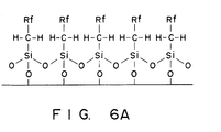
- Fig. 6A shows a model of a structural formula representing as an example the surface state of an optical film using as a binder a condensate having a fluoroalkyl group represented by chemical formula (I) given above.
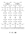
- Fig. 6B shows a model of a structural formula representing as another example the surface state of an optical film using as a binder a condensate having a fluoroalkyl group represented by chemical formula (II) given above.
- the value of X is set at 550 ⁇ m in which spectral luminous efficacy is best and the optical film 19 is formed in a thickness d of 1000A.
- the diameter of the fine magnesium fluoride particle 21 is smaller than 1000A.
- the magnesium fluoride particles are agglomerated within a coating solution used for forming the optical film so as to form large secondary particles, resulting in failure to form a homogeneous optical film 19.
- the silane compounds having a fluoroalkyl group which can be used for forming the optical film 19, include for example: CF 3 (CF 2 )s (CH 2 ) 2 Si (OR) 3
- R denote alkyl group or phenyl group.
- the optical film 19 is provided by a porous film consisting of fine magnesium fluoride particles 21 and a binder 22 consisting of a condensate of a silane compound having a fluoroalkyl group noted above, in which the alkoxy group may or may not be replaced by chlorine, or a co-condensate between a silane compound having a fluoroalkyl group and silicon or a metal oxide series compound
- the binder has a refractive index of 1.35 to 1.43, which is substantially equal to the refractive index (1.38) of magnesium fluoride.
- the refractive index of the optical film 19 is not significantly changed, even if the mixing ratio of the binder to the magnesium fluoride particles, i.e., binder/MgF 2 , is changed. It follows that the refractive index of the optical film 19 depends mainly on the porosity of the film.
- Figs. 7 to 9 are graphs reporting experimental data showing the relationship of reflactance, strength and porosity of the optical filter, and the binder/MgF 2 ratio, respectively.
- Fig. 10 is a graph reporting experimental data showing a change with time in the luminous reflectance.
- Fig. 7 includes curve 24 showing the relationship between the amount of a binder relative to the amount of magnesium fluoride particles, said binder consisting of a condensate of a silane compound having a fluoroalkyl group, and the luminous reflectance of the optical film prepared by using said binder.
- Fig. 7 also includes curve 25 denoting a control case.
- the data on the luminous reflectance in the control case are those under a stabilized condition reasonable time after the change in the initial stage.
- the reflectance it is preferable for the reflectance to be set at 1.0% or less. It follows that the amount of the binder should be at most 11 times as much as the amount of the magnesium fluoride particles, as seen from curve 24 of Fig. 7. On the other hand, curve 25 of Fig. 7 indicates that the amount of the silicon dioxide binder should be at most 0.25 time as much as the amount of the magnesium fluoride particles.
- the experimental data given in Fig. 7 support that the binder defined in the present invention can be used in a broader range of the amount and can be used in a larger amount, compared with the binder used in the conventional optical film for preventing an external light reflection.
- Fig. 8 includes curve 26 showing the relationship between the amount of a binder relative to the amount of magnesium fluoride particles, said binder consisting of a condensate of a silane compound having a fluoroalkyl group, and the mechanical strength of the optical film prepared by using said binder.
- Concerning the mechanical strength of the optical film the conventional optical film using a binder of the particular silicon dioxide noted previously is substantially equal to the optical film used in the present invention, though the data on the conventional optical film are not shown in Fig. 8. It is practically nesessary for the optical film formed on the surface of the vacuum envelope of a cathode ray tube to have a pencil hardness of at least 6H.
- Fig. 8 shows that, in order to form an optical film having a desired mechanical strength, it is preferable to use a binder in an amount at least 0.25 time as much as that of the magnesium fluoride particles.
- the amount of the binder is preferable to set the amount of the binder to fall within a range of between 0.25 and 11 times as much as the amount of the fine magnesium fluoride particles in order to form an optical film of a preferred reflectance and a desired mechanical strength by using fine magnesium fluoride particles and a binder consisting of a condensate of a silane compound having a fluoroalkyl group.
- a binder consisting of a condensate of a silane compound having a fluoroalkyl group.
- the optical film used in the present invention essentially differs from the conventional optical film using silicon dioxide as a binder.
- Fig. 9 is a graph showing the relationship between the porosity of the optical film and the amount of a binder relative to the amount of the fine magnesium fluoride particles, said binder consisting of a condensate of a silane compound having a fluoroalkyl group.
- a binder in an amount falling within a range of between 0.25 and 11, preferably between 0.5 and 11, times as much as the amount of the fine magnesium fluoride particles in order to form an optical film exhibiting a desired reflectance and a desired mechanical strength.
- the desirable porosity of the optical film should fall within a range of between 4.5 and 36%, more desirably between 8 and 27%, as apparent from curve 27 shown in Fig. 9.
- Fig. 10 is a graph showing a change with time in the luminous reflectance at a temperature of 25 C and a relative humidity of 90% with respect to an optical film used in the present invention (curve 29) and a conventional optical film using the particular silicon dioxide described previously as a binder (curve 28).
- a binder consisting of a condensate of a silane compound having a fluoroalkyl group was used in an amount of 0.25% by weight based on the amount of the fine magnesium fluoride particles in the case of the present invention (curve 29).
- the optical film used in the present invention is free from a change with time in the luminous reflectance.
- the luminous reflectance is greatly changed with time in the case of the conventional optical film using silicon dioxide as a binder.
- the magnesium fluoride particles are bonded to each other by a silicon matrix containing a siloxane bond having a fluoroalkyl group. It is considered reasonable to understand that the strong hydrophobic property of the fluoroalkyl group serves to prevent water from entering the pores of the porous thin film.
- the porous optical film used in the present invention contains a binder consisting of a condensate of a silane compound having a fluoroalkyl group or a co-condensate between the particular silane compound and silicon or a metal oxide series compound.
- the particular binder used in the present invention is substantially equal to magnesium fluoride in refractive index, making it possible to determine the amount of the binder relative to the amount of the magnesium fluoride particles in view of the desired porosity of the thin optical film. It follows that it is possible to prepare a thin optical film capable of sufficiently preventing an external light reflection.
- the binder used in the present invention is substantially equal in its bonding strength to silicon dioxide used as binder in the conventional optical film of a single layer structure, i.e., silicon dioxide prepared by hydrolyzing a silicon alkoxide, followed by applying a dehydrating-condensing reaction.
- silicon dioxide used as binder in the conventional optical film of a single layer structure
- the magnesium fluoride particles are bonded to each other in the present invention by a silicon matrix containing a siloxane bond having a hydrophobic fluoroalkyl group. It follows that the fluoroalkyl group serves to prevent water from entering the pores of the porous thin optical film, making it possible to prevent the luminous reflectance of the optical film from being changed with time.
- solution A to D shown in Table 1 Four kinds of solution A to D shown in Table 1 were prepared in the first step. Each of these solutions was subjected to aging for several hours while stirring the solution so as to carry out a hydrolyzing reaction and a dehydrating-condensing reaction to some extent.
- the outer surface of the panel used for a 25-inch color cathode ray tube was coated with the resultant solution by a spin coating method while rotating times of the panel is controlled so as to form a film having a thickness of 1000 ⁇ .
- the coated film was baked at 200°C for 20 minutes so as to form an optical film serving to prevent an external light reflection.
- the optical film thus formed exhibited a reflectance of 0.06 to 1.05, and a film hardness of 5H to 8H in pencil hardness.
- the resultant optical film was found to be substantially free from a change with time in the luminous reflectance.
- Example 2 Three kinds of solutions E to G as shown in Table 2 were prepared. As seen from Table 2, a co-condensate between a silane compound having a fluoroalkyl group and a silicon alkoxide was used as a binder in Example 2. As in Example 1, each of these solutions was subjected to aging for several hours while stirring the solution so as to carry out a hydrolyzing reaction and a dehydrating-condensing reaction to some extent. Then, the outer surface of the panel for a 25-inch color cathode ray tube was coated with the resultant solution by a spin coating method while rotating times of the panel so as to form a film having a thickness of 1000 ⁇ . The coated film was baked at 200° C for 20 minutes so as to form an optical film serving to prevent an external light reflection.
- the optical film thus formed exhibited a reflectance of about 0.4% in each of sample E, F, and G. Also, the resultant optical film was found to be substantially free from a change with time in the luminous reflectance. On the other hand, the mechanical strength of the optical film was also found to be satisfactory, i.e., 7H in pencil hardness. In conclusion, the optical film in Example 2 was satisfactory in each of the luminous reflectance and mechanical strength with respect to all the sample E, F and G.
- the optical film of the present invention even if formed in a clean room having a cleanness of 5000 class, were found to be substantially equal in the defect occurrence rate to the conventional optical film of a two layer structure formed in a clean room having a clanness of 1000 class. It follows that the optical film used in the present invention, which is adapted for a practical use, can be formed easily on a mass production basis.
- Example 2 a co-condensate between a silane compound having a fluoroalkyl group and a silicon alkoxide was used as a binder.
- a co-condensate between the particular silane compound and an alkoxide of a metal such as titanium or zirconium was used as a binder.
- the optical film it is possible for the optical film to contain a dye or pigment serving to impart a selective light absorbing function to the optical film.
- the dyes used in the present invention include, for example, acid rhodamine B and rhodamine B.
- the pigment used in the present invention include, for example, host palm pink mixture of cobalt (II) aluminate and cadmium red and pigment obtained by laking such dyes.
- the optical film it is possible for the optical film to contain fine particles of, for example, indium oxide or tin oxide so as to impart an electrical conductivity to the optical film. In this case, it is possible to prevent the optical film from being electrically charged, making it possible to prevent dust from being attached to the optical film and to prevent an electrical shock given to the human body.
- Fig. 11 shows a liquid crystal display device according to another embodiment of the present invention.
- the liquid crystal display device comprises a pair of mutually facing glass substrates 31, 32, electrode 33, 34 of predetermined patterns formed on the mutually facing inner surfaces of the glass substrates 31, 32, respectively, orientation film 35, 36 formed on the mutually facing inner surfaces of the glass substrates 31, 32, in a manner to cover the electrodes 33, 34, respectively, and spacers 37 arranged between the glass substrates 31 and 32 and fixed to the orientation films 35, 36.
- Each of the electrodes 33 and 34 is made of indium oxide tin oxide (ITO).
- the spacer 37 is formed of a thermosetting resin and determined the clearance between the glass substrates 31 and 32.
- the liquid crystal display device also comprises a liquid crystal material 38 filling the clearance, and a sealant 39 serving to seal the peripheral portion of the glass substrates 31, 32 having the liquid crystal material 38 loaded therein.
- the optical film 19 serving to prevent an external light reflection is formed to cover the outer surface of one of the glass substrates, i.e., the glass substrate 31 acting as the substrate of a display section of the liquid crystal display device.
- the optical film 19 was formed as follows. Specifically, the outer surface of the liquid crystal display device constructed as described above was sealed except for the outer surface of the electrode 31. Under this condition, the display device was dipped in the solution B shown in Table 1, followed by pulling up the display device at a controlled pulling rate so as to form a coating film having a thickness of 1000A on the surface of the electrode 31. Finally, the coating film was baked with a hot air of about 60 C for 40 minutes so as to form the optical film 19, as desired.
- the optical film 19 formed on the outer surface of the electrode 31 was found to exhibit a luminous reflectance of about 0.4% and a mechanical strength of 7H in pencil hardness. Further, the optical film 19 was found to be free from a change with time in the luminous reflectance.
Landscapes
- Physics & Mathematics (AREA)
- Nonlinear Science (AREA)
- Mathematical Physics (AREA)
- Chemical & Material Sciences (AREA)
- Crystallography & Structural Chemistry (AREA)
- General Physics & Mathematics (AREA)
- Optics & Photonics (AREA)
- Surface Treatment Of Optical Elements (AREA)
- Vessels, Lead-In Wires, Accessory Apparatuses For Cathode-Ray Tubes (AREA)
- Devices For Indicating Variable Information By Combining Individual Elements (AREA)
Applications Claiming Priority (2)
| Application Number | Priority Date | Filing Date | Title |
|---|---|---|---|
| JP2195896A JPH0482145A (ja) | 1990-07-24 | 1990-07-24 | 表示装置 |
| JP195896/90 | 1990-07-24 |
Publications (3)
| Publication Number | Publication Date |
|---|---|
| EP0468423A2 true EP0468423A2 (fr) | 1992-01-29 |
| EP0468423A3 EP0468423A3 (en) | 1992-04-29 |
| EP0468423B1 EP0468423B1 (fr) | 1996-11-13 |
Family
ID=16348793
Family Applications (1)
| Application Number | Title | Priority Date | Filing Date |
|---|---|---|---|
| EP91112272A Expired - Lifetime EP0468423B1 (fr) | 1990-07-24 | 1991-07-22 | Dispositif de visualisation |
Country Status (6)
| Country | Link |
|---|---|
| US (1) | US5281893A (fr) |
| EP (1) | EP0468423B1 (fr) |
| JP (1) | JPH0482145A (fr) |
| KR (1) | KR950008106B1 (fr) |
| DE (1) | DE69123094T2 (fr) |
| TW (1) | TW208066B (fr) |
Cited By (4)
| Publication number | Priority date | Publication date | Assignee | Title |
|---|---|---|---|---|
| US5539275A (en) * | 1992-04-06 | 1996-07-23 | Matsushita Electric Corporation | Display device and a method for producing the same |
| EP1333497A3 (fr) * | 2002-02-01 | 2005-01-05 | Seiko Epson Corporation | Substrat de circuit, dispositif électro-optique et appareil électronique |
| WO2006030848A1 (fr) | 2004-09-16 | 2006-03-23 | Nikon Corporation | Film optique mince de mgf2 contenant un liant d'oxyde de silicium amorphe, dispositif optique le contenant et procede de production du film optique mince de mgf2 |
| EP1818693A1 (fr) * | 2006-02-14 | 2007-08-15 | DSMIP Assets B.V. | Cadre comprenant plaque de verre revêtue d'une couche anti-reflet |
Families Citing this family (17)
| Publication number | Priority date | Publication date | Assignee | Title |
|---|---|---|---|---|
| JP2546054B2 (ja) * | 1990-10-24 | 1996-10-23 | 三菱電機株式会社 | 低反射膜付陰極線管 |
| EP0585819B1 (fr) * | 1992-08-31 | 1997-04-16 | Sumitomo Cement Co. Ltd. | Couche de revêtement anti-réfléchissante et anti-statique pour un tube à rayons cathodiques |
| EP0596531B1 (fr) * | 1992-11-06 | 1997-07-09 | Kabushiki Kaisha Toshiba | Couche antiréfléchissante et dispositif d'affichage contenant cette couche |
| US5981059A (en) * | 1995-04-03 | 1999-11-09 | Southwall Technologies, Inc. | Multi-layer topcoat for an optical member |
| JP3808917B2 (ja) * | 1995-07-20 | 2006-08-16 | オリンパス株式会社 | 薄膜の製造方法及び薄膜 |
| US5990984A (en) * | 1995-11-16 | 1999-11-23 | Viratec Thin Films, Inc. | Coated polymer substrate with matching refractive index and method of making the same |
| JPH09326240A (ja) * | 1996-06-05 | 1997-12-16 | Sony Corp | 表示素子用反射防止フィルター |
| US6210858B1 (en) | 1997-04-04 | 2001-04-03 | Fuji Photo Film Co., Ltd. | Anti-reflection film and display device using the same |
| US5851674A (en) * | 1997-07-30 | 1998-12-22 | Minnesota Mining And Manufacturing Company | Antisoiling coatings for antireflective surfaces and methods of preparation |
| US6277485B1 (en) | 1998-01-27 | 2001-08-21 | 3M Innovative Properties Company | Antisoiling coatings for antireflective surfaces and methods of preparation |
| US20030179455A1 (en) * | 2002-03-22 | 2003-09-25 | Jeffrey Hunt | Fingerprint resistant anti-reflection coatings for plastic substrates |
| US20040209072A1 (en) * | 2002-08-09 | 2004-10-21 | Inka Henze | Cleaning-friendly article with an easily cleanable, heat-resistant surface coating |
| DE10236728A1 (de) * | 2002-08-09 | 2004-02-26 | Schott Glas | Reinigungsfreundliche Vorrichtung |
| KR100533418B1 (ko) * | 2003-07-10 | 2005-12-05 | 엘지.필립스 디스플레이 주식회사 | 칼라 음극선관용 패널 및 그 제조 방법 |
| US20050282457A1 (en) * | 2004-06-18 | 2005-12-22 | Taiwan Micro Display Corp. | Display face plate and its method of making |
| CN100480736C (zh) * | 2004-09-16 | 2009-04-22 | 尼康股份有限公司 | MgF2光学薄膜和具备该薄膜的光学组件以及该薄膜的制造方法 |
| JPWO2008001675A1 (ja) * | 2006-06-27 | 2009-11-26 | 株式会社ニコン | 光学多層薄膜、光学素子、及び光学多層薄膜の製造方法 |
Family Cites Families (8)
| Publication number | Priority date | Publication date | Assignee | Title |
|---|---|---|---|---|
| JPS58172243A (ja) * | 1982-04-02 | 1983-10-11 | Asahi Glass Co Ltd | ガラス表面の処理剤 |
| JPS58211701A (ja) * | 1982-06-04 | 1983-12-09 | Asahi Glass Co Ltd | 低反射率ガラス |
| DE3228735A1 (de) * | 1982-07-31 | 1984-02-02 | Hazemag Dr. E. Andreas GmbH & Co, 4400 Münster | Fahrbare oder verfahrbare zerkleinerungsanlage |
| JPS60218747A (ja) * | 1984-04-13 | 1985-11-01 | Hitachi Ltd | ブラウン管の製造方法 |
| JPS6110043A (ja) * | 1984-06-26 | 1986-01-17 | Asahi Glass Co Ltd | 防汚性を有する低反射率ガラス |
| JPH0719550B2 (ja) * | 1987-08-06 | 1995-03-06 | 日本電気株式会社 | 反射防止型陰極線管の製造方法 |
| JP3072991B2 (ja) * | 1988-05-13 | 2000-08-07 | 株式会社日立製作所 | 陰極線管 |
| JPH02115801A (ja) * | 1988-10-26 | 1990-04-27 | Asahi Optical Co Ltd | 染色可能な反射防止膜組成物 |
-
1990
- 1990-07-24 JP JP2195896A patent/JPH0482145A/ja active Pending
-
1991
- 1991-07-08 TW TW080105291A patent/TW208066B/zh active
- 1991-07-22 US US07/733,806 patent/US5281893A/en not_active Expired - Lifetime
- 1991-07-22 EP EP91112272A patent/EP0468423B1/fr not_active Expired - Lifetime
- 1991-07-22 DE DE69123094T patent/DE69123094T2/de not_active Expired - Fee Related
- 1991-07-24 KR KR1019910012760A patent/KR950008106B1/ko not_active Expired - Fee Related
Cited By (9)
| Publication number | Priority date | Publication date | Assignee | Title |
|---|---|---|---|---|
| US5539275A (en) * | 1992-04-06 | 1996-07-23 | Matsushita Electric Corporation | Display device and a method for producing the same |
| EP1333497A3 (fr) * | 2002-02-01 | 2005-01-05 | Seiko Epson Corporation | Substrat de circuit, dispositif électro-optique et appareil électronique |
| WO2006030848A1 (fr) | 2004-09-16 | 2006-03-23 | Nikon Corporation | Film optique mince de mgf2 contenant un liant d'oxyde de silicium amorphe, dispositif optique le contenant et procede de production du film optique mince de mgf2 |
| EP1791002A4 (fr) * | 2004-09-16 | 2010-06-09 | Nikon Corp | Film optique mince de mgf<sb>2</sb>contenant un liant d'oxyde de silicium amorphe, dispositif optique le contenant et procede de production du film optique mince de mgf<sb>2</sb> |
| EP2637047A3 (fr) * | 2004-09-16 | 2014-02-26 | Nikon Corporation | Film mince optique MgF2 comprenant un liant d'oxyde de silicium amorphe, élément optique équipé de celui-ci et procédé de production de film mince optique MgF2 |
| EP2990839A1 (fr) * | 2004-09-16 | 2016-03-02 | Nikon Corporation | Film mince optique mgf2 comprenant un liant d'oxyde de silicium amorphe, élément optique équipé de celui-ci et procédé de production de film mince optique mgf2 |
| US9915761B2 (en) | 2004-09-16 | 2018-03-13 | Nikon Corporation | Optical system having optical thin film including amorphous silicon oxide-based binder |
| EP1818693A1 (fr) * | 2006-02-14 | 2007-08-15 | DSMIP Assets B.V. | Cadre comprenant plaque de verre revêtue d'une couche anti-reflet |
| WO2007093341A1 (fr) * | 2006-02-14 | 2007-08-23 | Dsm Ip Assets B.V. | Revetements antireflecteurs |
Also Published As
| Publication number | Publication date |
|---|---|
| DE69123094D1 (de) | 1996-12-19 |
| TW208066B (fr) | 1993-06-21 |
| EP0468423B1 (fr) | 1996-11-13 |
| JPH0482145A (ja) | 1992-03-16 |
| EP0468423A3 (en) | 1992-04-29 |
| KR950008106B1 (ko) | 1995-07-25 |
| KR920003396A (ko) | 1992-02-29 |
| DE69123094T2 (de) | 1997-04-03 |
| US5281893A (en) | 1994-01-25 |
Similar Documents
| Publication | Publication Date | Title |
|---|---|---|
| EP0468423B1 (fr) | Dispositif de visualisation | |
| KR920002531B1 (ko) | 화상표시면판 및 그 제조방법 | |
| EP0445686A2 (fr) | Dispositif d'affichage | |
| US5218268A (en) | Optical filter for cathode ray tube | |
| JPH0883581A (ja) | 表示装置の表面基板処理膜とその製造方法 | |
| JP2001101984A (ja) | カラー陰極線管 | |
| US5965975A (en) | Conductive anti-reflection film, fabrication method thereof, and cathode ray tube therewith | |
| JPH07134955A (ja) | 表示装置およびその反射率調整方法 | |
| KR20020090090A (ko) | 광 전송이 조정 가능한 비디오 디스플레이 스크린용정전기 방지/반사 방지 코팅 | |
| JP3223261B2 (ja) | 陰極線管およびその製造方法 | |
| KR100330315B1 (ko) | 도전성반사방지막및음극선관 | |
| EP0972297B1 (fr) | Procede de fabrication d'un revetement sur un ecran d'affichage et dispositif d'affichage comprenant ledit ecran a revetement | |
| JPH0680903A (ja) | 帯電防止・高屈折率膜形成用塗料および帯電防止・反射防止膜付き透明材料積層体および陰極線管 | |
| JP2000515310A (ja) | 色フィルタ層を有するカラー表示装置 | |
| US6642647B2 (en) | Cathode ray tube having a pigment on a panel front face | |
| JPH06139964A (ja) | 機能性フィルム付陰極線管 | |
| JPH05292437A (ja) | 投写型テレビ | |
| EP0426037A2 (fr) | Tube à rayons cathodiques | |
| JPH06344489A (ja) | 帯電防止・高屈折率膜形成用塗料、および帯電防止・反射防止膜付き透明積層体および陰極線管 | |
| JPH05203804A (ja) | 反射防止膜および表示装置 | |
| KR100342040B1 (ko) | 고휘도음극선관 | |
| KR20030026807A (ko) | 굴절률이 개선된 비디오 디스플레이 스크린을 위한 정전기방지/반사 방지코팅 | |
| JPH03179649A (ja) | 反射防止型陰極線管およびその製造方法 | |
| KR100394054B1 (ko) | 음극선관 | |
| JP3466089B2 (ja) | 導電性反射防止膜および陰極線管 |
Legal Events
| Date | Code | Title | Description |
|---|---|---|---|
| PUAI | Public reference made under article 153(3) epc to a published international application that has entered the european phase |
Free format text: ORIGINAL CODE: 0009012 |
|
| 17P | Request for examination filed |
Effective date: 19910819 |
|
| AK | Designated contracting states |
Kind code of ref document: A2 Designated state(s): DE FR GB |
|
| PUAL | Search report despatched |
Free format text: ORIGINAL CODE: 0009013 |
|
| AK | Designated contracting states |
Kind code of ref document: A3 Designated state(s): DE FR GB |
|
| 17Q | First examination report despatched |
Effective date: 19940927 |
|
| GRAG | Despatch of communication of intention to grant |
Free format text: ORIGINAL CODE: EPIDOS AGRA |
|
| GRAH | Despatch of communication of intention to grant a patent |
Free format text: ORIGINAL CODE: EPIDOS IGRA |
|
| GRAH | Despatch of communication of intention to grant a patent |
Free format text: ORIGINAL CODE: EPIDOS IGRA |
|
| GRAA | (expected) grant |
Free format text: ORIGINAL CODE: 0009210 |
|
| AK | Designated contracting states |
Kind code of ref document: B1 Designated state(s): DE FR GB |
|
| REF | Corresponds to: |
Ref document number: 69123094 Country of ref document: DE Date of ref document: 19961219 |
|
| ET | Fr: translation filed | ||
| PLBE | No opposition filed within time limit |
Free format text: ORIGINAL CODE: 0009261 |
|
| STAA | Information on the status of an ep patent application or granted ep patent |
Free format text: STATUS: NO OPPOSITION FILED WITHIN TIME LIMIT |
|
| 26N | No opposition filed | ||
| REG | Reference to a national code |
Ref country code: GB Ref legal event code: 746 Effective date: 19981015 |
|
| REG | Reference to a national code |
Ref country code: FR Ref legal event code: D6 |
|
| REG | Reference to a national code |
Ref country code: GB Ref legal event code: IF02 |
|
| PGFP | Annual fee paid to national office [announced via postgrant information from national office to epo] |
Ref country code: DE Payment date: 20070719 Year of fee payment: 17 |
|
| PGFP | Annual fee paid to national office [announced via postgrant information from national office to epo] |
Ref country code: GB Payment date: 20070718 Year of fee payment: 17 |
|
| PGFP | Annual fee paid to national office [announced via postgrant information from national office to epo] |
Ref country code: FR Payment date: 20070710 Year of fee payment: 17 |
|
| GBPC | Gb: european patent ceased through non-payment of renewal fee |
Effective date: 20080722 |
|
| PG25 | Lapsed in a contracting state [announced via postgrant information from national office to epo] |
Ref country code: DE Free format text: LAPSE BECAUSE OF NON-PAYMENT OF DUE FEES Effective date: 20090203 |
|
| REG | Reference to a national code |
Ref country code: FR Ref legal event code: ST Effective date: 20090331 |
|
| PG25 | Lapsed in a contracting state [announced via postgrant information from national office to epo] |
Ref country code: GB Free format text: LAPSE BECAUSE OF NON-PAYMENT OF DUE FEES Effective date: 20080722 |
|
| PG25 | Lapsed in a contracting state [announced via postgrant information from national office to epo] |
Ref country code: FR Free format text: LAPSE BECAUSE OF NON-PAYMENT OF DUE FEES Effective date: 20080731 |