EP0468456B1 - Informationsaufzeichnungs- und/oder Wiedergabegerät und Methode - Google Patents
Informationsaufzeichnungs- und/oder Wiedergabegerät und Methode Download PDFInfo
- Publication number
- EP0468456B1 EP0468456B1 EP91112342A EP91112342A EP0468456B1 EP 0468456 B1 EP0468456 B1 EP 0468456B1 EP 91112342 A EP91112342 A EP 91112342A EP 91112342 A EP91112342 A EP 91112342A EP 0468456 B1 EP0468456 B1 EP 0468456B1
- Authority
- EP
- European Patent Office
- Prior art keywords
- medium
- probe electrode
- voltage
- current value
- probe
- Prior art date
- Legal status (The legal status is an assumption and is not a legal conclusion. Google has not performed a legal analysis and makes no representation as to the accuracy of the status listed.)
- Expired - Lifetime
Links
- 238000000034 method Methods 0.000 title claims description 44
- 239000000523 sample Substances 0.000 claims description 130
- 230000008859 change Effects 0.000 claims description 14
- 238000006243 chemical reaction Methods 0.000 claims description 9
- 230000003321 amplification Effects 0.000 claims 2
- 238000003199 nucleic acid amplification method Methods 0.000 claims 2
- 239000000758 substrate Substances 0.000 description 27
- 238000010586 diagram Methods 0.000 description 15
- 230000007246 mechanism Effects 0.000 description 9
- 230000003446 memory effect Effects 0.000 description 8
- 230000007423 decrease Effects 0.000 description 6
- 239000000463 material Substances 0.000 description 6
- 230000015654 memory Effects 0.000 description 6
- 230000005684 electric field Effects 0.000 description 5
- 239000010408 film Substances 0.000 description 5
- 238000001514 detection method Methods 0.000 description 4
- 239000000126 substance Substances 0.000 description 4
- 238000013459 approach Methods 0.000 description 3
- 238000003776 cleavage reaction Methods 0.000 description 3
- 229910052751 metal Inorganic materials 0.000 description 3
- 239000002184 metal Substances 0.000 description 3
- 230000000737 periodic effect Effects 0.000 description 3
- BASFCYQUMIYNBI-UHFFFAOYSA-N platinum Chemical compound [Pt] BASFCYQUMIYNBI-UHFFFAOYSA-N 0.000 description 3
- 230000007017 scission Effects 0.000 description 3
- 238000004611 spectroscopical analysis Methods 0.000 description 3
- 238000004364 calculation method Methods 0.000 description 2
- 150000001786 chalcogen compounds Chemical class 0.000 description 2
- 238000010276 construction Methods 0.000 description 2
- 230000000694 effects Effects 0.000 description 2
- 230000008020 evaporation Effects 0.000 description 2
- 238000001704 evaporation Methods 0.000 description 2
- 239000011521 glass Substances 0.000 description 2
- 229910052737 gold Inorganic materials 0.000 description 2
- 239000010931 gold Substances 0.000 description 2
- 239000010439 graphite Substances 0.000 description 2
- 229910002804 graphite Inorganic materials 0.000 description 2
- 150000002894 organic compounds Chemical class 0.000 description 2
- 229910052697 platinum Inorganic materials 0.000 description 2
- 230000008569 process Effects 0.000 description 2
- 239000002994 raw material Substances 0.000 description 2
- 239000004065 semiconductor Substances 0.000 description 2
- 239000010409 thin film Substances 0.000 description 2
- 238000012935 Averaging Methods 0.000 description 1
- OKTJSMMVPCPJKN-UHFFFAOYSA-N Carbon Chemical compound [C] OKTJSMMVPCPJKN-UHFFFAOYSA-N 0.000 description 1
- 229910052581 Si3N4 Inorganic materials 0.000 description 1
- 229910021417 amorphous silicon Inorganic materials 0.000 description 1
- 230000008901 benefit Effects 0.000 description 1
- 238000004040 coloring Methods 0.000 description 1
- 150000001875 compounds Chemical class 0.000 description 1
- 239000004020 conductor Substances 0.000 description 1
- 229910052802 copper Inorganic materials 0.000 description 1
- 238000012937 correction Methods 0.000 description 1
- 239000013078 crystal Substances 0.000 description 1
- 238000005520 cutting process Methods 0.000 description 1
- 238000013500 data storage Methods 0.000 description 1
- 238000000354 decomposition reaction Methods 0.000 description 1
- 230000003247 decreasing effect Effects 0.000 description 1
- 238000011161 development Methods 0.000 description 1
- 239000003792 electrolyte Substances 0.000 description 1
- 238000010894 electron beam technology Methods 0.000 description 1
- 230000006870 function Effects 0.000 description 1
- 230000004927 fusion Effects 0.000 description 1
- PCHJSUWPFVWCPO-UHFFFAOYSA-N gold Chemical compound [Au] PCHJSUWPFVWCPO-UHFFFAOYSA-N 0.000 description 1
- 230000006872 improvement Effects 0.000 description 1
- 239000000696 magnetic material Substances 0.000 description 1
- 239000010445 mica Substances 0.000 description 1
- 229910052618 mica group Inorganic materials 0.000 description 1
- 229910052750 molybdenum Inorganic materials 0.000 description 1
- 230000003287 optical effect Effects 0.000 description 1
- 239000002245 particle Substances 0.000 description 1
- 238000005498 polishing Methods 0.000 description 1
- 229920000642 polymer Polymers 0.000 description 1
- 230000009467 reduction Effects 0.000 description 1
- 230000004044 response Effects 0.000 description 1
- HQVNEWCFYHHQES-UHFFFAOYSA-N silicon nitride Chemical compound N12[Si]34N5[Si]62N3[Si]51N64 HQVNEWCFYHHQES-UHFFFAOYSA-N 0.000 description 1
- 229910052709 silver Inorganic materials 0.000 description 1
- 239000010944 silver (metal) Substances 0.000 description 1
- 230000001360 synchronised effect Effects 0.000 description 1
- 230000007704 transition Effects 0.000 description 1
- WFKWXMTUELFFGS-UHFFFAOYSA-N tungsten Chemical compound [W] WFKWXMTUELFFGS-UHFFFAOYSA-N 0.000 description 1
- 229910052721 tungsten Inorganic materials 0.000 description 1
- 239000010937 tungsten Substances 0.000 description 1
Images


Classifications
-
- G—PHYSICS
- G11—INFORMATION STORAGE
- G11B—INFORMATION STORAGE BASED ON RELATIVE MOVEMENT BETWEEN RECORD CARRIER AND TRANSDUCER
- G11B9/00—Recording or reproducing using a method not covered by one of the main groups G11B3/00 - G11B7/00; Record carriers therefor
- G11B9/12—Recording or reproducing using a method not covered by one of the main groups G11B3/00 - G11B7/00; Record carriers therefor using near-field interactions; Record carriers therefor
- G11B9/14—Recording or reproducing using a method not covered by one of the main groups G11B3/00 - G11B7/00; Record carriers therefor using near-field interactions; Record carriers therefor using microscopic probe means, i.e. recording or reproducing by means directly associated with the tip of a microscopic electrical probe as used in Scanning Tunneling Microscopy [STM] or Atomic Force Microscopy [AFM] for inducing physical or electrical perturbations in a recording medium; Record carriers or media specially adapted for such transducing of information
- G11B9/1418—Disposition or mounting of heads or record carriers
- G11B9/1427—Disposition or mounting of heads or record carriers with provision for moving the heads or record carriers relatively to each other or for access to indexed parts without effectively imparting a relative movement
- G11B9/1436—Disposition or mounting of heads or record carriers with provision for moving the heads or record carriers relatively to each other or for access to indexed parts without effectively imparting a relative movement with provision for moving the heads or record carriers relatively to each other
- G11B9/1445—Disposition or mounting of heads or record carriers with provision for moving the heads or record carriers relatively to each other or for access to indexed parts without effectively imparting a relative movement with provision for moving the heads or record carriers relatively to each other switching at least one head in operating function; Controlling the relative spacing to keep the head operative, e.g. for allowing a tunnel current flow
-
- G—PHYSICS
- G11—INFORMATION STORAGE
- G11B—INFORMATION STORAGE BASED ON RELATIVE MOVEMENT BETWEEN RECORD CARRIER AND TRANSDUCER
- G11B9/00—Recording or reproducing using a method not covered by one of the main groups G11B3/00 - G11B7/00; Record carriers therefor
- G11B9/12—Recording or reproducing using a method not covered by one of the main groups G11B3/00 - G11B7/00; Record carriers therefor using near-field interactions; Record carriers therefor
- G11B9/14—Recording or reproducing using a method not covered by one of the main groups G11B3/00 - G11B7/00; Record carriers therefor using near-field interactions; Record carriers therefor using microscopic probe means, i.e. recording or reproducing by means directly associated with the tip of a microscopic electrical probe as used in Scanning Tunneling Microscopy [STM] or Atomic Force Microscopy [AFM] for inducing physical or electrical perturbations in a recording medium; Record carriers or media specially adapted for such transducing of information
- G11B9/1418—Disposition or mounting of heads or record carriers
- G11B9/1427—Disposition or mounting of heads or record carriers with provision for moving the heads or record carriers relatively to each other or for access to indexed parts without effectively imparting a relative movement
- G11B9/1436—Disposition or mounting of heads or record carriers with provision for moving the heads or record carriers relatively to each other or for access to indexed parts without effectively imparting a relative movement with provision for moving the heads or record carriers relatively to each other
- G11B9/1454—Positioning the head or record carrier into or out of operative position or across information tracks; Alignment of the head relative to the surface of the record carrier
-
- B—PERFORMING OPERATIONS; TRANSPORTING
- B82—NANOTECHNOLOGY
- B82Y—SPECIFIC USES OR APPLICATIONS OF NANOSTRUCTURES; MEASUREMENT OR ANALYSIS OF NANOSTRUCTURES; MANUFACTURE OR TREATMENT OF NANOSTRUCTURES
- B82Y10/00—Nanotechnology for information processing, storage or transmission, e.g. quantum computing or single electron logic
-
- Y—GENERAL TAGGING OF NEW TECHNOLOGICAL DEVELOPMENTS; GENERAL TAGGING OF CROSS-SECTIONAL TECHNOLOGIES SPANNING OVER SEVERAL SECTIONS OF THE IPC; TECHNICAL SUBJECTS COVERED BY FORMER USPC CROSS-REFERENCE ART COLLECTIONS [XRACs] AND DIGESTS
- Y10—TECHNICAL SUBJECTS COVERED BY FORMER USPC
- Y10S—TECHNICAL SUBJECTS COVERED BY FORMER USPC CROSS-REFERENCE ART COLLECTIONS [XRACs] AND DIGESTS
- Y10S977/00—Nanotechnology
- Y10S977/84—Manufacture, treatment, or detection of nanostructure
- Y10S977/849—Manufacture, treatment, or detection of nanostructure with scanning probe
-
- Y—GENERAL TAGGING OF NEW TECHNOLOGICAL DEVELOPMENTS; GENERAL TAGGING OF CROSS-SECTIONAL TECHNOLOGIES SPANNING OVER SEVERAL SECTIONS OF THE IPC; TECHNICAL SUBJECTS COVERED BY FORMER USPC CROSS-REFERENCE ART COLLECTIONS [XRACs] AND DIGESTS
- Y10—TECHNICAL SUBJECTS COVERED BY FORMER USPC
- Y10S—TECHNICAL SUBJECTS COVERED BY FORMER USPC CROSS-REFERENCE ART COLLECTIONS [XRACs] AND DIGESTS
- Y10S977/00—Nanotechnology
- Y10S977/84—Manufacture, treatment, or detection of nanostructure
- Y10S977/849—Manufacture, treatment, or detection of nanostructure with scanning probe
- Y10S977/85—Scanning probe control process
- Y10S977/851—Particular movement or positioning of scanning tip
-
- Y—GENERAL TAGGING OF NEW TECHNOLOGICAL DEVELOPMENTS; GENERAL TAGGING OF CROSS-SECTIONAL TECHNOLOGIES SPANNING OVER SEVERAL SECTIONS OF THE IPC; TECHNICAL SUBJECTS COVERED BY FORMER USPC CROSS-REFERENCE ART COLLECTIONS [XRACs] AND DIGESTS
- Y10—TECHNICAL SUBJECTS COVERED BY FORMER USPC
- Y10S—TECHNICAL SUBJECTS COVERED BY FORMER USPC CROSS-REFERENCE ART COLLECTIONS [XRACs] AND DIGESTS
- Y10S977/00—Nanotechnology
- Y10S977/84—Manufacture, treatment, or detection of nanostructure
- Y10S977/849—Manufacture, treatment, or detection of nanostructure with scanning probe
- Y10S977/86—Scanning probe structure
- Y10S977/861—Scanning tunneling probe
-
- Y—GENERAL TAGGING OF NEW TECHNOLOGICAL DEVELOPMENTS; GENERAL TAGGING OF CROSS-SECTIONAL TECHNOLOGIES SPANNING OVER SEVERAL SECTIONS OF THE IPC; TECHNICAL SUBJECTS COVERED BY FORMER USPC CROSS-REFERENCE ART COLLECTIONS [XRACs] AND DIGESTS
- Y10—TECHNICAL SUBJECTS COVERED BY FORMER USPC
- Y10S—TECHNICAL SUBJECTS COVERED BY FORMER USPC CROSS-REFERENCE ART COLLECTIONS [XRACs] AND DIGESTS
- Y10S977/00—Nanotechnology
- Y10S977/84—Manufacture, treatment, or detection of nanostructure
- Y10S977/88—Manufacture, treatment, or detection of nanostructure with arrangement, process, or apparatus for testing
- Y10S977/881—Microscopy or spectroscopy, e.g. sem, tem
Definitions
- the present invention relates to an apparatus and a method for recording and/or reproducing of the kind defined by the features of claims 1 and 12, respectively.
- the invention can be suitably used in apparatus and method for recording and/or reproducing to which a technique such as a scanning tunnel microscope or the like has been applied.
- STM scanning tunnel microscope
- the STM uses the principle that when a bias voltage is applied between a probe (probe electrode) of a metal and a conductive substance and the probe is allowed to approach until a distance of about 1 nm, a tunnel current flows.
- the tunnel current is very sensitive to a change in distance between them.
- the recording and reproduction at a high density can be sufficiently performed on the atom order (sub-nanometer).
- the recording/reproducing apparatus disclosed in JP-A-61-80536 atomic particles adsorbed onto the medium surface are eliminated by an electron beam or the like and the writing operation is executed and the data is reproduced by the STM.
- the recording and reproduction are executed by the STM by using a thin film layer as a recording layer made of a material such as ⁇ electron system organic compound or chalcogen compound class having a memory effect for a switching characteristic of a voltage current (JP-A-63-161552, JP-A-63-161553).
- a recording bit size is equal to 10 nm
- the recording and reproduction of a large capacity of 10 12 bits/cm 2 can be performed.
- the US-A-4 575 822 is concerned with a method and means for data storage using tunnel current data read out.
- the gap between the probe and the medium (dielectric layer 14 made from silicon nitride) is corrected based on an undulation information of the surface of the medium obtained by initial scanning. That is, in this document the gap between the probe and the medium is kept constant by an open-end control based on the undulation information.
- the probe In case a large vibration is applied to the apparatus respectively to the probe/medium the probe, however, may collide with the medium and may be damaged or damage the medium.
- the JP-A-1133239 is concerned with an apparatus for controlling the distance between the probe and the medium such that the current flowing between the probe and the medium is kept constant. More particularly, a servo-system for controlling this spacing between the conductive tip and the recording layer is used.
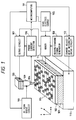
- Fig. 1 is a diagram showing a recording and/or reproducing apparatus according to a preferred embodiment of the invention.
- the recording/reproducing apparatus comprises: a probe electrode 104 which is arranged such that a tip of the probe electrode is close to the surface of a recording medium 102; a bias electric source 105 as means for applying a voltage between a substrate electrode 101 arranged on the back surface of the recording medium 102 and the probe electrode 104; a record/erasure signal generator 108; an adder 114 for adding outputs of the bias electric source 105 and the generator 108 and for applying between the electrode 104 and the medium 105; a probe current detector 106 to detect a current flowing between the recording medium 102 and the probe electrode 104; a longitudinal direction driving mechanism 103 for driving the probe electrode in the longitudinal direction (Z direction) to fluctuate a distance between the probe electrode 104 and the recording medium 102; and a servo circuit 107 to output a control signal to drive the longitudinal direction driving mechanism 103 on the basis of the voltage applied by the voltage applying means and the current detected by the probe current detector 106 in a manner such that a current which is
- An epitaxial growth plane of gold or a graphite cleavage plane on a flat substrate made of a glass or mica or the like can be used as a substrate electrode 101.
- Squarilium-bis-6-octyl azulene (hereinafter, abbreviated to "SOAZ”) is used as a recording medium 102.
- SOAZ Squarilium-bis-6-octyl azulene
- a built-up film of two layers of monomolecular films is formed on the surface of the substrate electrode 101 by a Langmuir-Blodgett's technique.
- a probe electrode 104 it is possible to use an electrode which is obtained by electrolyte polishing a tungsten line or the like or by mechanically cutting a platinum line or the like and whose tip is sharp (radius of curvature is less than 1 ⁇ m) and which is conductive.
- a PZT device or the like is used as a longitudinal direction driving mechanism 103, a bias voltage of about 1 V is applied between the substrate electrode 101 and the probe electrode 104 by the bias electric source 105, and a probe current flowing between them is detected by the probe current detector 106.
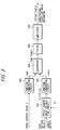
- Fig. 2 is a block diagram of the servo circuit 107.
- reference numeral 801 denotes a preset current value calculation circuit to calculate a set current value I 0 for an applied bias voltage value V and a distance set value Z 0 .
- a calculating method in the above case differs depending on current-voltage characteristics between the probe electrode 104 and the substrate electrode 101. For instance, when a tunnel current characteristic or a field emission current characteristic is exhibited, the set current value I 0 is calculated by the following equations.
- A, B, C, D denote constants which are predetermined by substances constructing the electrode and the recording medium.
- Reference numerals 802 and 803 denote function conversion circuits for obtaining signals logI and logI 0 by, for instance, logarithm converting a detection probe current value I and the set current value I 0 , respectively; 804 a subtracter for calculating a difference (logI - logI 0 ) between those signals and for outputting; 805 and 806 denote a filter and an amplifier (gain G) for an output of the subtracter 804.
- a signal G(logI - logI 0 ) which is generated from the amplifier 806 is supplied to the longitudinal direction driving mechanism control means 103.
- the sign of the gain G by the amplifier 806 is selected so as to drive in such a direction that the probe electrode 104 is away from the substrate electrode 101 when I > I 0 and that the probe electrode 104 contrarily approaches the substrate electrode 101 when I ⁇ I 0 . Due to this, the probe current value I is controlled so as to be always equal to the set current value for the applied bias voltage V. By controlling as mentioned above, even if the applied bias voltage V is changed as will be explained hereinlater, a resistance characteristic between the electrodes 101 and 104 is not changed, so that the distance between the probe electrode 104 and the substrate electrode 101 can be held constant.
- the tracking control by the probe electrode 104 is performed by driving the probe electrode 104 by the microcomputer 111 through an XY scan drive circuit 110 on the basis of the output of the probe current detector 106.
- the bias electric source 105 is also controlled by the microcomputer 111.
- the probe electrode 104 is driven by the longitudinal direction driving mechanism 103 so as to approach a desired position of the recording medium 102 until a distance of about sub-nanometer. Subsequently, a signal from the record/erasure signal generator 108 is applied between the substrate electrode 101 and the probe electrode 104 through the adder 114. The recording/erasing operations are executed at a desired position of the recording medium 102 which is close to the tip of the probe electrode 104. In a manner similar to the above, upon reproduction, a bias voltage for reading is applied between the substrate electrode 101 and the probe electrode 104 by the bias electric source 105 and the reproducing operation is executed at a desired position of the recording medium 102 which is close to the tip of the probe electrode 104.
- a method of controlling the distance between the probe electrode and the recording medium in the recording/reproducing method there are the following methods: a method whereby the recording/reproducing operations are executed while controlling the distance so as to make the probe current constant; a method whereby a current mean value which is obtained by averaging the current values which change due to the presence or absence of the recording is used as a reference and the distance is controlled so as to obtain such a reference value; and a method whereby upon recording, a mean value of the current at a time point before the current is enhanced for recording is held as a reference value and the distance is controlled so as to obtain such a reference value.
- Figs. 3A and 4A relate to the former case.
- Figs. 3B and 4B relate to the latter case.
- Figs. 3A and 3B show the case of the medium in which the recording is performed by a change in resistance value.
- Figs. 4A and 4B show the case of the medium in which the recording is executed by a change in shape.
- Each diagram shows a state when the applied voltage between the electrodes 101 and 104 has sequentially been increased from the left.
- the distance between the probe electrode 104 and the recording medium 102 or a conductive recording medium 402 increases in a process to increase the applied voltage V in order to perform the recording operation to the recording medium 102 or 402 and the electric field and potential decrease by an amount corresponding to the increase in distance. Therefore, there are problems such that the voltage is not efficiently applied and that a recording bit diameter increases because the voltage is applied in a wide range in correspondence to the increase in the distance.
- Fig. 5 is an explanatory diagram of a method of controlling the position in the longitudinal direction of the probe electrode 104 upon recording.
- Fig. 5 shows the control method in a manner similar to Figs. 3A and 3B.
- the distance between the probe electrode 104 and the substrate electrode 101 is held constant by the control of the longitudinal direction driving mechanism 103 by the servo circuit 107.
- the electrical memory effect can be caused by a lower applied voltage (for instance, the threshold voltage V th ) without losses of the electric field and potential due to an increase in distance between the probe electrode 104 and the substrate electrode 101 in association with an increase in applied voltage V, such losses cannot be avoided by the control to make the probe current I constant as mentioned above.
- the recording bit diameter also decreases because the distance between the probe electrode 104 and the substrate electrode 101 doesn't increase.
- the recording is executed by the applied voltage (V > V th ) exceeding the threshold voltage V th .
- V > V th the threshold voltage
- R OFF in the off state of a recording portion 115 changes (decreases) to a resistance value R ON in the on state
- Fig. 7 is an explanatory diagram of a method of controlling the position in the longitudinal direction of the probe electrode upon reproduction.
- the substrate electrode 101 is constructed by an atom array of a conductive crystal cleavage plane or the like and has a periodic structure on the surface.
- the bias electric source 105 is constructed in a manner such that when the recording state of the recording medium 102 on the substrate electrode 101 is reproduced by scanning the probe electrode 104, a bias electric source 604 for reproducing and a bias electric source 605 for tracking are alternately switched by a bias voltage switching circuit 606 in accordance with a switching signal from a reproduction/tracking switching signal generator 607 and the switched source is used.
- the recording state is reproduced by the bias for reproducing and the periodic structure of the surface of the substrate electrode 101 is detected by the bias for tracking, thereby executing the tracking control.
- the position in the longitudinal direction of the probe electrode 104 in a manner such that the probe current value is always equal to the set current value for the applied bias voltage, a change in distance between the probe electrode 104 and the substrate electrode 101 due to the switching of the bias voltage is eliminated.
- the longitudinal direction position control amount of the probe electrode 104 directly reflects the recording state and the periodic structure for tracking.
- the operation of the embodiment will now be summarized below.
- a voltage signal which is equal to or higher than a predetermined threshold level which causes the memory effect in the recording medium is applied, a change in electrical characteristic and physical and chemical changes occur in the recording medium portion, so that information is recorded in this portion.
- the distance between the probe electrode and the recording medium is controlled in a manner such that a current which is equal to the value of current flowing for the applied voltage in the case where the distance between the probe electrode and the recording medium is made constant flows between the probe electrode and the recording medium. Therefore, the distance between the probe electrode and the recording medium is held constant even if a voltage fluctuation of the threshold level or less occurs.
- the resistance value between the probe electrode and the recording medium decreases due to the change in electrical characteristics and the physical and chemical changes by such a memory effect. Therefore, under the control as mentioned above, the distance between the probe electrode and the recording medium increases by only a supplementary amount of such a decreased amount.
- the distance between the probe electrode and the recording medium is held constant under the foregoing control.
- the resistance value between the probe electrode and the recording medium decreases and the distance between the probe electrode and the recording medium is controlled so as to increase by only a supplementary amount of such a decrease amount. That is, a control amount in the above case indicates the recorded information, thereby executing the reproduction.
- the distance between the probe electrode and the recording medium is set to an enough small value and is held constant excluding the recording information portion by the foregoing control and the electric field between the probe electrode and the recording medium is stably held. Therefore, the recording and reproducing operations are efficiently executed at a high S/N ratio and a low error ratio by the stable electric field and by a small recording bit diameter.
- the recording and reproducing operations are executed without causing no damage of the probe electrode and the recording medium due to an excessive current flowing between them.
- Fig. 8 is an explanatory diagram of another embodiment of a method of controlling the position in the longitudinal direction of the probe electrode upon reproduction.
- a DC bias by a DC bias electric source 704 is modulated by a bias modulating circuit 705 and a resultant modulated bias is used as a bias for reproduction.
- Only the modulation component in a reproduction probe current signal I p derived is extracted by a synchronous detection circuit 706.
- the noises in the reproduction signal is reduced and the detection of the recording state by a spectroscopic method (information regarding an electron state is obtained from a dI p /dV signal) is executed.
- the position control in the longitudinal direction of the probe electrode 104 is executed in a manner such that the probe electrode current value I p is always equal to the set current value for the applied bias voltage V.
- the control amount of the position in the longitudinal direction of the probe electrode 101 directly reflects the recording state.
- the concept of the invention is not limited to such an example. It is also possible to construct in a manner such that a voltage which is equal to or higher than a certain threshold value is applied to the conductive recording medium 402 having a flat surface as shown in Fig. 6, thereby locally changing the surface shape of the recording medium 402 into a concave/convex shape by fusion, evaporation, decomposition, compound, or change in orienting direction.
- Fig. 6 shows in a manner similar to Figs. 4A and 4B. The effect of the invention will be obviously understood from Fig. 6.
- the following materials can be mentioned: an HOPG (Highly-Oriented-Pyrolytic-Graphite) cleavage substrate; an Si wafer; a thin metal film of Au, Ag, Pt, Mo, Cu, etc. which has been evaporation deposited in a vacuum state or which has been epitaxially grown; and glass metal of Rh 25 Zr 75 , Co 35 Tb 65 , or the like.
- HOPG Highly-Oriented-Pyrolytic-Graphite
- the distance between the probe electrode and the recording medium can be adjusted. Therefore, there are the following effects: (1) the recording signal can be efficiently applied; (2) the recording bit diameter can be reduced; (3) the damages of the tip of the probe and the medium of the recording portion upon recording can be prevented; and (4) various reproducing methods of applying the modulation to the bias such as tracking, improvement of an S/N ratio, spectroscopic method, etc. can be stably realized.
Landscapes
- Measurement Of Length, Angles, Or The Like Using Electric Or Magnetic Means (AREA)
- Semiconductor Memories (AREA)
Claims (17)
- Vorrichtung zum Aufzeichnen und/oder Reproduzieren von Information auf ein/von einem Medium (102, 402) über eine Sondenelektrode (104), umfassend:- eine Spannungsanlegeeinrichtung (105, 108, 114) zum Anlegen einer Spannung zwischen Medium und Sondenelektrode,- eine Abstandsjustiereinrichtung (103, 106) zum Justieren eines Abstands zwischen dem Medium und der Sondenelektrode in der Weise, daß der Stromfluß zwischen dem Medium und der Sondenelektrode beim Anlegen der Spannung zwischen Medium und Sondenelektrode eine vorbestimmte Stromstärke wird,- eine Stromstärkenänderungseinrichtung (801) zum Ändern der vorbestimmten Stromstärke,dadurch gekennzeichnet, daß
die Stromstärkenänderungseinrichtung (801) die vorbestimmte Stromstärke ändert, indem ein gewünschter Abstand zwischen dem Medium und einer Spitze der Sondenelektrode und der Wert der zwischen das Medium und die Sondenelektrode durch die Spannungsanlegeeinrichtung angelegten Spannung berücksichtigt werden. - Vorrichtung nach Anspruch 1, bei der
die Spannungsanlegeeinrichtung (105, 108, 114) zwischen das Medium (102, 402) und die Sondenelektrode (104) eine konstante Spannung legt, die die Kennwerte des Mediums veranlaßt, sich nicht zu ändern, wenn Information reproduziert wird. - Vorrichtung nach Anspruch 1, bei der
die Spannungsanlegeeinrichtung (105, 108, 114) eine Spannung zwischen das Medium (102, 402) und die Sondenelektrode (104) legt, die die Kennwerte des Mediums veranlaßt, sich zu ändern, wenn Information aufgezeichnet wird. - Vorrichtung nach einem der Ansprüche 1 bis 3, bei der die Abstandsjustiereinrichtung (103, 106) aufweist:- eine Sondenstrom-Detektiereinrichtung (106) zum Nachweisen der Stromstärke zwischen dem Medium (102, 402) und der Sondenelektrode (104),- eine erste Funktionswandlereinrichtung (802) zum logarithmischen Umsetzen der von der Sondenstrom-Detektiereinrichtung nachgewiesenen Stromstärke, um ein erstes logarithmisches Umwandlungssignal (log I) auszugeben,- eine zweite Funktionsumsetzeinrichtung (803) zum logarithmischen Umsetzen der vorbestimmten Stromstärke, um ein zweites logarithmisches Umwandlungssignal (log I0) auszugeben,- eine Subtrahiereinrichtung (804) zum Bilden einer Differenz zwischen dem ersten und dem zweiten logarithmischem Umwandlungssignal, um ein Differenzsignal auszugeben,- eine Verstärkungseinrichtung (806) zum Verstärken des Differenzsignals mit einem vorbestimmten Verstärkungsfaktor, und- eine Änderungseinrichtung zum Ändern des Abstands zwischen dem Medium und der Sondenelektrode auf der Grundlage des von der Verstärkungseinrichtung verstärkten Differenzsignals.
- Vorrichtung nach einem der Ansprüche 1 bis 4, bei der
die Stromstärkenänderungseinrichtung (801) die vorbestimmte Stromstärke in der Weise ändert, daß ein Verhältnis der zwischen die Sondenelektrode (104) und das Medium (102, 402) angelegten Spannung und der vorbestimmten Stromstärke stets konstant wird. - Vorrichtung nach einem der Ansprüche 1 bis 5, bei der
der zwischen dem Medium (102, 402) und der Sondenelektrode (104) fließende Strom ein Tunnelstrom ist. - Vorrichtung nach einem der Ansprüche 1 bis 5, bei der
der zu der Sondenelektrode (104) fließende Strom ein Feldemissionsstrom ist. - Vorrichtung nach einem der Ansprüche 1 bis 7, bei der
die Spannungsanlegeeinrichtung (105, 108, 114) aufweist:- eine elektrische Vorspannungsquelle (105) zum Erzeugen einer Vorspannung, um die Information von dem Medium (102, 402) nachzuweisen,- eine Signalgeneratoreinrichtung (108) zum Generieren eines Signals zwecks Aufzeichnung oder Löschung der Information auf das/von dem Medium über die Sondenelektrode (104),- eine Addiereinrichtung (114) zum Addieren eines Ausgangssignals der elektrischen Vorspannungsquelle und eines Ausgangssignals der Signalgeneratoreinrichtung, und zum Anlegen zwischen das Medium und die Sondenelektrode. - Vorrichtung nach einem der Ansprüche 1 bis 4, bei der
die Spannungsanlegeeinrichtung (105, 108, 114) aufweist:- eine elektrische Wiedergabe-Vorspannungsquelle (604) zum Erzeugen einer Vorspannung (V1), um die Information zu reproduzieren,- eine elektrische Spurverfolgungs-Vorspannungsquelle (605) zum Erzeugen einer Vorspannung (V2) für die Spurverfolgung, und- eine Schalteinrichtung (606) zum Schalten der Vorspannung für die Wiedergabe und der Vorspannung für die Spurverfolgung und zum Anlegen der geschalteten Vorspannungen zwischen das Medium (102, 402) und die Sondenelektrode (104). - Vorrichtung nach einem der Ansprüche 1 bis 7, bei der
die Spannungsanlegeeinrichtung (105, 108, 114) aufweist:
eine elektrische Gleich-Vorspannungsquelle (105) und eine Vorspannungs-Moduliereinrichtung zum Modulieren einer von der elektrischen Gleich-Vorspannungsquelle erzeugten Gleich-Vorspannung,und zum Anlegen der Spannung zwischen die Sondenelektrode (104) und das Medium (102, 402). - Verfahren zum Aufzeichnen und/oder Wiedergeben von Information auf ein/von einem Medium (102, 402) über eine Sondenelektrode, umfassend die Schritte:- Anlegen einer Spannung zwischen das Medium und die Sondenelektrode,- Justieren eines Abstands zwischen dem Medium und der Sondenelektrode in der Weise, daß ein zu der Sondenelektrode beim Anlegen der Spannung zwischen das Medium und die Sondenelektrode fließender Strom eine vorbestimmte Stromstärke annimmt,- Ändern der vorbestimmten Stromstärke nach Maßgabe der im Spannungsanlegeschritt angelegten Spannung,dadurch gekennzeichnet, daß
die vorbestimmte Stromstärke in dem Schritt zum Ändern der Stromstärke geändert wird, indem ein gewünschter Abstand zwischen dem Medium (102, 402) und einer Spitze der Sondenelektrode (104) ebenso berücksichtigt wird, wie der Spannungswert, der zwischen das Medium und die Sondenelektrode gelegt wird. - Verfahren nach Anspruch 11, bei dem
bei der Wiedergabe von Information während des Spannungsanlegeschritts zwischen das Medium und die Sondenelektrode (104) eine konstante Spannung gelegt wird, die veranlaßt, daß sich die Kennwerte des Mediums (102, 402) nicht ändern. - Verfahren nach Anspruch 11, bei dem
bei der Informationsaufzeichnung während des Spannungsanlegeschritts zwischen das Medium und die Sondenelektrode (104) eine konstante Spannung gelegt wird, die veranlaßt, daß sich die Kennwerte des Mediums (102, 402) ändern. - Verfahren nach einem der Ansprüche 11 bis 13, bei dem
der Abstands-Justierschritt folgende Schritte umfaßt:- Nachweisen der Stärke des zwischen dem Medium (102, 402) und der Sondenelektrode (104) fließenden Stroms,- logarithmisches Umsetzen der nachgewiesenen Stromstärke, um ein erstes logarithmisches Umwandlungssignal auszugeben,- logarithmisches Umsetzen der vorbestimmten Stromstärke, um ein zweites logarithmisches Umwandlungssignal auszugeben,- Nachweisen einer Differenz zwischen dem ersten und dem zweiten logarithmischen Umwandlungssignal, um ein Differenzsignal auszugeben,- Verstärken des Differenzsignals mit einem vorbestimmten Verstärkungsfaktor, und- Ändern des Abstands zwischen dem Medium und der Sondenelektrode auf der Grundlage des verstärkten Differenzsignals. - Verfahren nach einem der Ansprüche 11 bis 14, bei dem
die vorbestimmte Stromstärke in dem Stromstärke-Änderungsschritt in der Weise geändert wird, daß ein Verhältnis der zwischen die Sondenelektrode (104) und das Medium (102, 402) gelegten Spannung und der vorbestimmten Stromstärke stets konstant wird. - Verfahren nach einem der Ansprüche 11 bis 15, bei der
zwischen dem Medium (102, 402) und der Sondenelektrode (104) fließende Strom ein Tunnelstrom ist. - Verfahren nach einem der Ansprüche 11 bis 15, bei dem
der zu der Sondenelektrode (104) fließende Strom ein Feldemissionsstrom ist.
Applications Claiming Priority (2)
| Application Number | Priority Date | Filing Date | Title |
|---|---|---|---|
| JP2194825A JP2743213B2 (ja) | 1990-07-25 | 1990-07-25 | 記録及び/又は再生を行なう装置および方法 |
| JP194825/90 | 1990-07-25 |
Publications (3)
| Publication Number | Publication Date |
|---|---|
| EP0468456A2 EP0468456A2 (de) | 1992-01-29 |
| EP0468456A3 EP0468456A3 (en) | 1993-05-05 |
| EP0468456B1 true EP0468456B1 (de) | 1997-04-09 |
Family
ID=16330884
Family Applications (1)
| Application Number | Title | Priority Date | Filing Date |
|---|---|---|---|
| EP91112342A Expired - Lifetime EP0468456B1 (de) | 1990-07-25 | 1991-07-23 | Informationsaufzeichnungs- und/oder Wiedergabegerät und Methode |
Country Status (5)
| Country | Link |
|---|---|
| US (1) | US5289455A (de) |
| EP (1) | EP0468456B1 (de) |
| JP (1) | JP2743213B2 (de) |
| CA (1) | CA2047801C (de) |
| DE (1) | DE69125538T2 (de) |
Families Citing this family (50)
| Publication number | Priority date | Publication date | Assignee | Title |
|---|---|---|---|---|
| US5216661A (en) * | 1991-07-22 | 1993-06-01 | The Johns Hopkins University | Electron density storage device using a stm |
| DE4126497A1 (de) * | 1991-08-10 | 1993-02-11 | Basf Ag | Verfahren zur gezielten modifikation von festkoerperoberflaechen im nanometerbereich durch lokale delamination sowie verwendung des verfahrens zur speicherung von informationseinheiten |
| JPH06187675A (ja) * | 1992-09-25 | 1994-07-08 | Canon Inc | 情報処理装置、及びそれを用いる情報処理方法 |
| US5418771A (en) * | 1993-02-25 | 1995-05-23 | Canon Kabushiki Kaisha | Information processing apparatus provided with surface aligning mechanism between probe head substrate and recording medium substrate |
| JPH06251435A (ja) * | 1993-03-01 | 1994-09-09 | Canon Inc | 記録再生装置 |
| EP0615235B9 (de) * | 1993-03-09 | 2003-11-12 | Canon Kabushiki Kaisha | Informationsaufzeichnungsmethode und -gerät |
| US5453970A (en) * | 1993-07-13 | 1995-09-26 | Rust; Thomas F. | Molecular memory medium and molecular memory disk drive for storing information using a tunnelling probe |
| JP2923190B2 (ja) * | 1993-12-16 | 1999-07-26 | シャープ株式会社 | 高密度記録媒体及びその記録再生装置 |
| US5790495A (en) | 1994-05-06 | 1998-08-04 | Discovision Associates | Data generator assembly for retrieving stored data by comparing threshold signal with preprocessed signal having DC component |
| US5894468A (en) * | 1994-05-06 | 1999-04-13 | Discovision Associates | Data recovery with differentiation and partial integration stages to eliminate noises and DC offset level |
| US5723981A (en) * | 1994-08-29 | 1998-03-03 | Imec Vzw | Method for measuring the electrical potential in a semiconductor element |
| JP3581475B2 (ja) * | 1995-02-13 | 2004-10-27 | キヤノン株式会社 | 情報処理装置 |
| JP3576644B2 (ja) * | 1995-06-19 | 2004-10-13 | キヤノン株式会社 | 情報記録装置のプローブ及び記録媒体、並びにこれらを用いた情報記録方法 |
| US5757760A (en) * | 1996-01-18 | 1998-05-26 | Canon Kabushiki Kaisha | Information recording and/or reproducing apparatus and method for performing recording and/or reproduction of information by using probe |
| JP3679525B2 (ja) * | 1996-10-07 | 2005-08-03 | キヤノン株式会社 | 情報記録再生装置、および情報記録再生方法 |
| JP3827105B2 (ja) * | 1997-02-12 | 2006-09-27 | 株式会社モリタユージー | 天井裏設置型自動消火装置 |
| US7260051B1 (en) * | 1998-12-18 | 2007-08-21 | Nanochip, Inc. | Molecular memory medium and molecular memory integrated circuit |
| DE19912814C2 (de) * | 1999-03-22 | 2002-02-14 | Max Planck Gesellschaft | Verfahren und Vorrichtung zur Rastertunnelmikroskopie |
| US20020138301A1 (en) * | 2001-03-22 | 2002-09-26 | Thanos Karras | Integration of a portal into an application service provider data archive and/or web based viewer |
| US7002149B2 (en) * | 2001-11-26 | 2006-02-21 | Japan Science And Technology Agency | Delay time modulation femtosecond time-resolved scanning probe microscope apparatus |
| JP3680035B2 (ja) * | 2002-03-29 | 2005-08-10 | 株式会社東芝 | 磁気記録装置及び磁気記録方法 |
| KR100519772B1 (ko) * | 2002-10-14 | 2005-10-07 | 삼성전자주식회사 | 스핀 분극된 전자를 이용한 자성매체 및 자성매체를이용한 정보기록장치 및 기록방법 |
| JP4102280B2 (ja) * | 2002-10-14 | 2008-06-18 | 三星電子株式会社 | スピン分極電子を用いた磁性媒体及び磁性媒体への情報記録装置及び記録方法 |
| US7233517B2 (en) | 2002-10-15 | 2007-06-19 | Nanochip, Inc. | Atomic probes and media for high density data storage |
| US6985377B2 (en) * | 2002-10-15 | 2006-01-10 | Nanochip, Inc. | Phase change media for high density data storage |
| US20040150472A1 (en) * | 2002-10-15 | 2004-08-05 | Rust Thomas F. | Fault tolerant micro-electro mechanical actuators |
| US6982898B2 (en) * | 2002-10-15 | 2006-01-03 | Nanochip, Inc. | Molecular memory integrated circuit utilizing non-vibrating cantilevers |
| US7254108B2 (en) * | 2004-03-15 | 2007-08-07 | Hewlett-Packard Development Company, L.P. | Storage device including a probe having an electrically conductive tip portion for electrical contact with a storage medium |
| US20050243592A1 (en) * | 2004-04-16 | 2005-11-03 | Rust Thomas F | High density data storage device having eraseable bit cells |
| US7301887B2 (en) * | 2004-04-16 | 2007-11-27 | Nanochip, Inc. | Methods for erasing bit cells in a high density data storage device |
| US20050232061A1 (en) * | 2004-04-16 | 2005-10-20 | Rust Thomas F | Systems for writing and reading highly resolved domains for high density data storage |
| US7379412B2 (en) | 2004-04-16 | 2008-05-27 | Nanochip, Inc. | Methods for writing and reading highly resolved domains for high density data storage |
| US20050243660A1 (en) * | 2004-04-16 | 2005-11-03 | Rust Thomas F | Methods for erasing bit cells in a high density data storage device |
| US7463573B2 (en) * | 2005-06-24 | 2008-12-09 | Nanochip, Inc. | Patterned media for a high density data storage device |
| US20060291271A1 (en) * | 2005-06-24 | 2006-12-28 | Nanochip, Inc. | High density data storage devices having servo indicia formed in a patterned media |
| US7367119B2 (en) * | 2005-06-24 | 2008-05-06 | Nanochip, Inc. | Method for forming a reinforced tip for a probe storage device |
| US20070008865A1 (en) * | 2005-07-08 | 2007-01-11 | Nanochip, Inc. | High density data storage devices with polarity-dependent memory switching media |
| US7309630B2 (en) * | 2005-07-08 | 2007-12-18 | Nanochip, Inc. | Method for forming patterned media for a high density data storage device |
| US20070008866A1 (en) * | 2005-07-08 | 2007-01-11 | Nanochip, Inc. | Methods for writing and reading in a polarity-dependent memory switch media |
| US20070008867A1 (en) * | 2005-07-08 | 2007-01-11 | Nanochip, Inc. | High density data storage devices with a lubricant layer comprised of a field of polymer chains |
| US20070036060A1 (en) * | 2005-08-11 | 2007-02-15 | Tdk Corporation | Data recording method, data reproducing method, data recording apparatus, data reproducing apparatus, and information recording medium |
| US20080001075A1 (en) * | 2006-06-15 | 2008-01-03 | Nanochip, Inc. | Memory stage for a probe storage device |
| US20080175033A1 (en) * | 2007-01-19 | 2008-07-24 | Nanochip, Inc. | Method and system for improving domain stability in a ferroelectric media |
| US20080174918A1 (en) * | 2007-01-19 | 2008-07-24 | Nanochip, Inc. | Method and system for writing and reading a charge-trap media with a probe tip |
| US20080233672A1 (en) * | 2007-03-20 | 2008-09-25 | Nanochip, Inc. | Method of integrating mems structures and cmos structures using oxide fusion bonding |
| US20090129246A1 (en) * | 2007-11-21 | 2009-05-21 | Nanochip, Inc. | Environmental management of a probe storage device |
| US20090294028A1 (en) * | 2008-06-03 | 2009-12-03 | Nanochip, Inc. | Process for fabricating high density storage device with high-temperature media |
| CN101324785B (zh) * | 2008-07-17 | 2010-06-09 | 浙江大学 | 用于扫描隧道显微镜的纯钨材质微纳探针制备控制系统 |
| US20100039729A1 (en) * | 2008-08-14 | 2010-02-18 | Nanochip, Inc. | Package with integrated magnets for electromagnetically-actuated probe-storage device |
| US20100039919A1 (en) * | 2008-08-15 | 2010-02-18 | Nanochip, Inc. | Cantilever Structure for Use in Seek-and-Scan Probe Storage |
Citations (1)
| Publication number | Priority date | Publication date | Assignee | Title |
|---|---|---|---|---|
| US575822A (en) * | 1897-01-26 | Garment-hook |
Family Cites Families (12)
| Publication number | Priority date | Publication date | Assignee | Title |
|---|---|---|---|---|
| JPS57109149A (en) * | 1980-12-26 | 1982-07-07 | Toshiba Corp | Signal recording system |
| JPS5922251A (ja) * | 1982-07-29 | 1984-02-04 | Toshiba Corp | 記録装置 |
| JPS6180536A (ja) * | 1984-09-14 | 1986-04-24 | ゼロツクス コーポレーシヨン | 原子規模密度情報記緑および読出し装置並びに方法 |
| JP2556492B2 (ja) * | 1986-12-24 | 1996-11-20 | キヤノン株式会社 | 再生装置及び再生法 |
| JP2556491B2 (ja) * | 1986-12-24 | 1996-11-20 | キヤノン株式会社 | 記録装置及び記録法 |
| US5001409A (en) * | 1987-10-09 | 1991-03-19 | Hitachi, Ltd. | Surface metrological apparatus |
| JP2523144B2 (ja) * | 1987-11-18 | 1996-08-07 | 株式会社日立製作所 | 情報記録再生装置および情報記録媒体 |
| US4916688A (en) * | 1988-03-31 | 1990-04-10 | International Business Machines Corporation | Data storage method using state transformable materials |
| US4956817A (en) * | 1988-05-26 | 1990-09-11 | Quanscan, Inc. | High density data storage and retrieval system |
| NL8802335A (nl) * | 1988-09-21 | 1990-04-17 | Philips Nv | Werkwijze en inrichting voor het op sub-mikron schaal bewerken van een materiaal-oppervlak. |
| JP2916167B2 (ja) * | 1989-07-11 | 1999-07-05 | オリンパス光学工業株式会社 | 走査型分光顕微鏡及び走査型分光情報検出方法 |
| JP2744338B2 (ja) * | 1990-08-01 | 1998-04-28 | キヤノン株式会社 | 情報読取り及び/又は入力を行なう装置及び方法 |
-
1990
- 1990-07-25 JP JP2194825A patent/JP2743213B2/ja not_active Expired - Fee Related
-
1991
- 1991-07-23 EP EP91112342A patent/EP0468456B1/de not_active Expired - Lifetime
- 1991-07-23 US US07/734,700 patent/US5289455A/en not_active Expired - Fee Related
- 1991-07-23 DE DE69125538T patent/DE69125538T2/de not_active Expired - Fee Related
- 1991-07-24 CA CA002047801A patent/CA2047801C/en not_active Expired - Fee Related
Patent Citations (1)
| Publication number | Priority date | Publication date | Assignee | Title |
|---|---|---|---|---|
| US575822A (en) * | 1897-01-26 | Garment-hook |
Also Published As
| Publication number | Publication date |
|---|---|
| DE69125538T2 (de) | 1997-10-09 |
| EP0468456A3 (en) | 1993-05-05 |
| CA2047801C (en) | 1997-08-26 |
| DE69125538D1 (de) | 1997-05-15 |
| JP2743213B2 (ja) | 1998-04-22 |
| EP0468456A2 (de) | 1992-01-29 |
| JPH0482037A (ja) | 1992-03-16 |
| CA2047801A1 (en) | 1992-01-26 |
| US5289455A (en) | 1994-02-22 |
Similar Documents
| Publication | Publication Date | Title |
|---|---|---|
| US5289455A (en) | Information recording and/or reproducing apparatus | |
| EP0513790B1 (de) | Gerät zur Informationsverarbeitung | |
| EP0510579B1 (de) | Informationsaufzeichnungs- oder Wiedergabegerät | |
| US5432771A (en) | Information recording/reproducing apparatus for performing recording/reproduction of information by using probe | |
| JPH06251435A (ja) | 記録再生装置 | |
| EP0541978A2 (de) | Informationsverarbeitungsgerät | |
| JP3029143B2 (ja) | 情報再生方法 | |
| US5805541A (en) | Circumferential data recording/reproducing with a microvibration scanning probe | |
| EP0640963B1 (de) | Aufzeichnungs und Wiedergabeverfahren und Gerät mit einer Rastersonde | |
| JP3044417B2 (ja) | 情報処理装置 | |
| JP3029503B2 (ja) | 記録方法および情報処理装置 | |
| JP2967308B2 (ja) | 微小カンチレバー型プローブ及びその製造方法、それを備えた表面観察装置及び情報処理装置 | |
| JP3095915B2 (ja) | 情報処理装置 | |
| JP3217493B2 (ja) | 情報記録再生装置 | |
| JP3004823B2 (ja) | 情報処理装置 | |
| JP3093946B2 (ja) | 記録媒体 | |
| JP3078141B2 (ja) | 記録装置および記録再生装置 | |
| JP2968610B2 (ja) | 情報記録再生装置 | |
| JPH08249733A (ja) | 情報処理装置 | |
| JPH05342647A (ja) | 情報処理装置 | |
| JPH06195774A (ja) | 情報処理装置および走査型プローブ顕微鏡と複数プローブ制御方法 | |
| JPH05135416A (ja) | 情報記録装置 | |
| JPH09198727A (ja) | 情報記録再生装置 | |
| JPH06267120A (ja) | マルチプローブヘッド及びこれを具備する記録再生装置 | |
| JPH0552510A (ja) | 情報処理装置及び走査型トンネル電子顕微鏡 |
Legal Events
| Date | Code | Title | Description |
|---|---|---|---|
| PUAI | Public reference made under article 153(3) epc to a published international application that has entered the european phase |
Free format text: ORIGINAL CODE: 0009012 |
|
| AK | Designated contracting states |
Kind code of ref document: A2 Designated state(s): BE CH DE ES FR GB IT LI NL SE |
|
| PUAL | Search report despatched |
Free format text: ORIGINAL CODE: 0009013 |
|
| AK | Designated contracting states |
Kind code of ref document: A3 Designated state(s): BE CH DE ES FR GB IT LI NL SE |
|
| 17P | Request for examination filed |
Effective date: 19930928 |
|
| 17Q | First examination report despatched |
Effective date: 19950721 |
|
| GRAG | Despatch of communication of intention to grant |
Free format text: ORIGINAL CODE: EPIDOS AGRA |
|
| GRAH | Despatch of communication of intention to grant a patent |
Free format text: ORIGINAL CODE: EPIDOS IGRA |
|
| GRAH | Despatch of communication of intention to grant a patent |
Free format text: ORIGINAL CODE: EPIDOS IGRA |
|
| GRAA | (expected) grant |
Free format text: ORIGINAL CODE: 0009210 |
|
| AK | Designated contracting states |
Kind code of ref document: B1 Designated state(s): BE CH DE ES FR GB IT LI NL SE |
|
| PG25 | Lapsed in a contracting state [announced via postgrant information from national office to epo] |
Ref country code: NL Effective date: 19970409 Ref country code: LI Effective date: 19970409 Ref country code: ES Free format text: THE PATENT HAS BEEN ANNULLED BY A DECISION OF A NATIONAL AUTHORITY Effective date: 19970409 Ref country code: CH Effective date: 19970409 Ref country code: BE Effective date: 19970409 |
|
| REG | Reference to a national code |
Ref country code: CH Ref legal event code: EP |
|
| REF | Corresponds to: |
Ref document number: 69125538 Country of ref document: DE Date of ref document: 19970515 |
|
| ITF | It: translation for a ep patent filed | ||
| ET | Fr: translation filed | ||
| PG25 | Lapsed in a contracting state [announced via postgrant information from national office to epo] |
Ref country code: SE Effective date: 19970709 |
|
| NLV1 | Nl: lapsed or annulled due to failure to fulfill the requirements of art. 29p and 29m of the patents act | ||
| REG | Reference to a national code |
Ref country code: CH Ref legal event code: PL |
|
| PLBE | No opposition filed within time limit |
Free format text: ORIGINAL CODE: 0009261 |
|
| STAA | Information on the status of an ep patent application or granted ep patent |
Free format text: STATUS: NO OPPOSITION FILED WITHIN TIME LIMIT |
|
| 26N | No opposition filed | ||
| REG | Reference to a national code |
Ref country code: GB Ref legal event code: IF02 |
|
| PGFP | Annual fee paid to national office [announced via postgrant information from national office to epo] |
Ref country code: FR Payment date: 20040708 Year of fee payment: 14 |
|
| PGFP | Annual fee paid to national office [announced via postgrant information from national office to epo] |
Ref country code: GB Payment date: 20040721 Year of fee payment: 14 |
|
| PGFP | Annual fee paid to national office [announced via postgrant information from national office to epo] |
Ref country code: DE Payment date: 20040806 Year of fee payment: 14 |
|
| PG25 | Lapsed in a contracting state [announced via postgrant information from national office to epo] |
Ref country code: IT Free format text: LAPSE BECAUSE OF NON-PAYMENT OF DUE FEES;WARNING: LAPSES OF ITALIAN PATENTS WITH EFFECTIVE DATE BEFORE 2007 MAY HAVE OCCURRED AT ANY TIME BEFORE 2007. THE CORRECT EFFECTIVE DATE MAY BE DIFFERENT FROM THE ONE RECORDED. Effective date: 20050723 Ref country code: GB Free format text: LAPSE BECAUSE OF NON-PAYMENT OF DUE FEES Effective date: 20050723 |
|
| PG25 | Lapsed in a contracting state [announced via postgrant information from national office to epo] |
Ref country code: DE Free format text: LAPSE BECAUSE OF NON-PAYMENT OF DUE FEES Effective date: 20060201 |
|
| GBPC | Gb: european patent ceased through non-payment of renewal fee |
Effective date: 20050723 |
|
| PG25 | Lapsed in a contracting state [announced via postgrant information from national office to epo] |
Ref country code: FR Free format text: LAPSE BECAUSE OF NON-PAYMENT OF DUE FEES Effective date: 20060331 |
|
| REG | Reference to a national code |
Ref country code: FR Ref legal event code: ST Effective date: 20060331 |