EP0469603A2 - Dispositif pour former une couche mince de supraconducteur composite en oxyde - Google Patents
Dispositif pour former une couche mince de supraconducteur composite en oxyde Download PDFInfo
- Publication number
- EP0469603A2 EP0469603A2 EP91112948A EP91112948A EP0469603A2 EP 0469603 A2 EP0469603 A2 EP 0469603A2 EP 91112948 A EP91112948 A EP 91112948A EP 91112948 A EP91112948 A EP 91112948A EP 0469603 A2 EP0469603 A2 EP 0469603A2
- Authority
- EP
- European Patent Office
- Prior art keywords
- laser beam
- scanning
- target
- substrate
- thin film
- Prior art date
- Legal status (The legal status is an assumption and is not a legal conclusion. Google has not performed a legal analysis and makes no representation as to the accuracy of the status listed.)
- Granted
Links
Images


Classifications
-
- C—CHEMISTRY; METALLURGY
- C23—COATING METALLIC MATERIAL; COATING MATERIAL WITH METALLIC MATERIAL; CHEMICAL SURFACE TREATMENT; DIFFUSION TREATMENT OF METALLIC MATERIAL; COATING BY VACUUM EVAPORATION, BY SPUTTERING, BY ION IMPLANTATION OR BY CHEMICAL VAPOUR DEPOSITION, IN GENERAL; INHIBITING CORROSION OF METALLIC MATERIAL OR INCRUSTATION IN GENERAL
- C23C—COATING METALLIC MATERIAL; COATING MATERIAL WITH METALLIC MATERIAL; SURFACE TREATMENT OF METALLIC MATERIAL BY DIFFUSION INTO THE SURFACE, BY CHEMICAL CONVERSION OR SUBSTITUTION; COATING BY VACUUM EVAPORATION, BY SPUTTERING, BY ION IMPLANTATION OR BY CHEMICAL VAPOUR DEPOSITION, IN GENERAL
- C23C14/00—Coating by vacuum evaporation, by sputtering or by ion implantation of the coating forming material
- C23C14/22—Coating by vacuum evaporation, by sputtering or by ion implantation of the coating forming material characterised by the process of coating
- C23C14/24—Vacuum evaporation
- C23C14/28—Vacuum evaporation by wave energy or particle radiation
-
- H—ELECTRICITY
- H10—SEMICONDUCTOR DEVICES; ELECTRIC SOLID-STATE DEVICES NOT OTHERWISE PROVIDED FOR
- H10N—ELECTRIC SOLID-STATE DEVICES NOT OTHERWISE PROVIDED FOR
- H10N60/00—Superconducting devices
- H10N60/01—Manufacture or treatment
- H10N60/0268—Manufacture or treatment of devices comprising copper oxide
- H10N60/0296—Processes for depositing or forming copper oxide superconductor layers
- H10N60/0521—Processes for depositing or forming copper oxide superconductor layers by pulsed laser deposition, e.g. laser sputtering
Definitions
- This invention relates to a device for forming a compound oxide superconducting thin film, specifically to a device for forming a compound oxide superconducting thin film by laser evaporation.
- Compound oxide superconducting materials having the above-described high critical temperatures were originally prepared in sintered bodies by powder metallurgy. But the sintered bodies could not exhibit preferable characteristics, especially critical current density, etc. Recently processes for forming superconducting materials in thin films have been dominantly studied. Usually compound oxide superconducting thin films are formed on SrTi0 3 mono crystal substrates, MgO mono crystal substrates, etc. by various kinds of evaporation, such as vacuum evaporation, spattering, etc.
- the compound oxide thin film formed by various kinds of conventionally known evaporation do not generally exhibit sufficient superconductivity as formed.
- the post-annealing is performed for the purpose of supplementing oxygen due to the oxygen non-stoichiometry.
- Laser evaporation comprises irradiating a target with a high power laser beam, evaporating material of the target, and depositing the same on a substrate.
- the heating of the target, and that of the substrate can be controlled independently of each other. It is not always necessary to make the ambient atmosphere highly vacuum, It is possible to increase the film forming speed by selecting suitable conditions.
- laser evaporation is considered suitable to form compound oxide superconducting materials in thin films. It has been confirmed that the compound oxide superconducting films formed by laser evaporation without the above-described post-annealing exhibit useful superconductive characteristics. Laser evaporation is expected to be dominant in processes for forming oxide superconducting films.
- a sectional area to be contributed to the film formation by the plume is generally smaller than an area of a substrate.
- a thin film is formed by laser evaporation only on a part of the film forming surface of the substrate.
- a thin film which can exhibit effective superconductive characteristics is formed in about 10 mm-diameter at most, and such small thin film is not practical.
- This invention relates to a device for forming a thin film by laser evaporation, and an object of this invention is to provide a device for forming a thin film, especially a thin film of a compound oxide superconducting material, on a substrate having a larger film forming surface.
- the device according to this invention is a device for forming a compound oxide superconducting thin film by laser evaporation and is characterized by comprising a scanning optical system such as a rotary polygon mirror and a usually used unit as a film forming device.
- the device according to this invention has realized that a laser beam is caused to scan by, e.g., a rotary polygon mirror, so as to form over a larger area a superconducting thin film, and film formation over such layer area can not be formed by a fixed laser beam.
- a scanning direction of a laser beam by the scanning optical system by a laser beam is one dimension, it is preferable to transfer the substrate in direction perpendicularly to a direction of scanning of the laser beam to form a film on a substrate.
- the scanning optical system may be so arranged that a laser beam can be caused to scan two-dimensionally. This embodiment is shown in FIG. 4.
- a first galvanometer mirror deflects a laser beam in one direction
- a second galvanometer mirror causes the laser beam to scan in a direction perpendicular thereto, whereby two-dimensional scanning can be performed.
- This arrangement according to this invention does not require transfer of a substrate. This arrangement enables a laser beam spot on a target to scan over the target, and as the result, local consumption of the target can be prevented. In other words, one target can last longer, and substantial consumption of a target can be decreased.
- This invention is applicable to all thin film forming using laser evaporation, and the superconducting thin films to which this invention is especially effectively applied are oxide superconducting materials including La-Ba-Cu, Y-Ba-Cu, Bi- and TI-system oxides, which are formed on SrTi0 3 or MgO single-crystal substrate, etc.
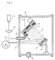
- FIG. 1 is a pictorial view of an arrangement of the device for forming a thin film according to a first embodiment of this invention.
- the interior of the film forming chamber is shown in a sectional view in Fig. 1.
- this device mainly comprises a film forming chamber 8 which houses a substrate holder 2 for holding a substrate 1 and a target holder 4 for holding a target 3, and has an exhaust port 5, an oxygen supply port 6 and a laser beam entrance window 7; and laser irradiating means including a laser 11 which has an optical system 10 and generates a laser beam, and a rotary polygon mirror 12.
- the substrate holder 2 is set on a translating device 20 for the substrate holder 2, which will be explained later, and is movable back and forth with respect to the sheet of FIG. 1.
- the oxygen supply port 6 is connected to a nozzle 6a so that oxygen gas is blown near to a film forming surface of the substrate 1.
- the optical system 10 converges a laser beam emitted from the laser 11 or expand a beam radius of the laser beam to supplement its output power.
- Optical system 10 is designed suitably to meet necessary film forming requirements.
- FIG. 2 shows a structure example of the transfer device 20 for the substrate holder 2 shown in Fig. 1.
- the transfer device 20 is laid on a side with a film forming surface of the substrate faced this way.
- the transfer device 20 mainly comprises a frame 21 having a predetermined sectional shape, and a plurality of pairs of guide rollers 22 with the rollers of each pair opposed to each other.
- the guide rollers 22 are arranged so as to engage in a pair of guide grooves 2a cut in both side walls of the plate-shaped substrate holder 2.
- Some of the guide rollers 22 are forcedly driven by driving means 24.
- the driving means 24 may be reversible to thereby reverse a transfer direction.
- the heater 23 comprises a plurality of rod-shaped heating bodies 23a arranged perpendicular to a transfer direction. Each of the rod-shaped heating bodies 23a can be individually controlled, so that temperature distributions can be formed in a transfer direction of the substrate holder 2.
- the transfer device 20 of the above-described structure is used as follows.
- the substrate holder 2 with a substrate 1 set on is inserted into the frame 21 so that the guide rollers 22 are engaged into a pair of guide grooves 2a.
- the frame 21 is placed as it is at a set position in the film forming chamber of FIG. 1.
- the driving means 24 is actuated to transfer the substrate 2 linearly.
- the heater 23 is turned on to heat the substrate 1 up to a required temperature.
- a substrate 1 and a target 3 are set on the substrate holder 2 and a target holder 4, and then the film forming chamber 8 is degassed. Subsequently, with the rotation the rotary polygon mirror 12, the laser 11 is actuated to irradiate a laser beam onto the target 3.
- the transfer device 20 is moved during the irradiation of the laser beam, so that plume 9 generated from the target 3 radiates all over the substrate.
- oxygen gas is blown from the nozzle 6a onto a film forming surface of the substrate 1.
- the inventors actually formed Y-B-C-0 system thin film using the same device as shown in FIGs. 1 and 2.
- the laser beam source an Ar-F pulse laser oscillator having an output energy density of 2 J/cm 2 on the surface of the target and 10 Hz frequency was used.
- the target a sintered body having a size of 15cm x 3cm x 1cm and made of YBa 2 Cu 3 0 x was used.
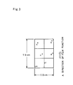
- 2 x 3 15 sheets of MgO(100) having a size of 5 cm x 5 cm substrates were located as shown in FIG. 3. The distance between the substrate and the target was set to be 5 cm.
- the interior of the film forming chanber was kept vacuum at 200 mTorr.
- Oxygen was blown onto the substrate from the nozzle at the rate of 30 cc/min.
- the film forming temperature was 700 C.
- the polygon mirror had 12 planes.
- the rotation speed was 5 rpm.
- the thin film forming was conducted for 50 minutes under these conditions.
- the thickness of the film Angstrom: ⁇
- the critical temperature Tc K
- the critical current density Jc A/cm 2
- FIG. 4 The arrangement of FIG. 4 is the same as that of the first embodiment of FIGs. 1 and 2 in that a substrate 1 is held by a substrate holder 2, a target 3 is held by a target holder (not shown), and these are housed in a film forming chamber 8 with a laser beam entrance window 7. It is also the same as in the first embodiment that an oxygen supply nozzle (not shown) is disposed near the substrate 1, and a laser beam from a laser beam source 11 is condensed by a lens 10. The following three points are differences of the second embodiment from the first one.
- a galvanometer mirror 40 is used as an optical system for the scanning of a laser beam (scanning in Y direction on the target).
- the galvanometer mirror 40 comprises a plane mirror 41 inserted in an optical path of the optical system, a shaft 42 fixed to the center of the plane mirror 41.
- electromagnetic reversible driving means 43 connected to the shaft 42.
- the galvanometer 40 is driven reversibly within a set range in the directions indicated by the arrows in FIG. 4, so that the incident angle of a laser beam with respect to the plane mirror 41 is varied, and the spot of the laser beam is caused to scan in the direction Y on the target 3.
- a galvanometer mirror 50 for deflecting a laser beam in the direction X.
- the galvanometer 50 comprises a plane mirror 51, a shaft 52, and a reversible driving means 53.
- the mirror 40 for the scanning in the direction Y is being driven, the mirror 50 for the scanning in the direction Y is driven at a relatively low speed.
- the target 3 does not have to be moved.
- the target 3 is irradiated with a laser beam over a large area, and accordingly the consumption of the target can be minimized.
- a homogeneous, high-quality superconducting thin film can be formed over a large area of a stationary substrate 1.
- the optical system for causing a laser beam to scan is not limited to the optical system of the type in which a reflecting mirror is movable, but instead an optical system of the type in which the optical refractive index is variable may be used.
- electrooptic crystals such as LiNb0 3
- electrooptic crystals can vary the refractive index by an electric field. It is possible to cause a laser beam to transmit through these crystal having electrodes so that the laser beam is caused to scan in the above-mentioned directions X, Y by applying a voltage to the electrodes.
- the deflection of a laser beam in the direction X can be performed by moving the laser beam source 11, because the scanning in the direction X is slower than in the direction Y.
- the device according to this invention is characterized in that a substrate for a thin film to be formed on is moved at a low speed in the direction X while causing the laser beam to scan in the direction Y by an optical system at a relatively high speed, or the optical axis of a laser beam is moved (or deflected) in the direction X at a low speed.
- the superconducting thin film formed by laser evaporation has little diffusion of a substrate material into a superconducting thin film and has accordingly high quality, because laser evaporation can omit post-annealing from the thin film forming process.
- the oxide superconducting thin film formed by the device according to this invention is suitably usable in various devices, such as a string of thin film devices, superconducting quantum interference devices (SQUIDs), etc.
Landscapes
- Chemical & Material Sciences (AREA)
- Engineering & Computer Science (AREA)
- Organic Chemistry (AREA)
- Physics & Mathematics (AREA)
- Toxicology (AREA)
- Materials Engineering (AREA)
- Mechanical Engineering (AREA)
- Metallurgy (AREA)
- Health & Medical Sciences (AREA)
- Chemical Kinetics & Catalysis (AREA)
- Optics & Photonics (AREA)
- Manufacturing & Machinery (AREA)
- Physical Vapour Deposition (AREA)
- Superconductors And Manufacturing Methods Therefor (AREA)
- Superconductor Devices And Manufacturing Methods Thereof (AREA)
- Oxygen, Ozone, And Oxides In General (AREA)
- Inorganic Compounds Of Heavy Metals (AREA)
- Crystals, And After-Treatments Of Crystals (AREA)
Applications Claiming Priority (6)
| Application Number | Priority Date | Filing Date | Title |
|---|---|---|---|
| JP20475890 | 1990-08-01 | ||
| JP20475890 | 1990-08-01 | ||
| JP204758/90 | 1990-08-01 | ||
| JP3205526A JPH05804A (ja) | 1990-08-01 | 1991-07-22 | 大面積複合酸化物超電導薄膜の成膜装置 |
| JP205526/91 | 1991-07-22 | ||
| JP20552691 | 1991-07-22 |
Publications (3)
| Publication Number | Publication Date |
|---|---|
| EP0469603A2 true EP0469603A2 (fr) | 1992-02-05 |
| EP0469603A3 EP0469603A3 (en) | 1992-06-03 |
| EP0469603B1 EP0469603B1 (fr) | 2000-03-29 |
Family
ID=26514629
Family Applications (1)
| Application Number | Title | Priority Date | Filing Date |
|---|---|---|---|
| EP91112948A Expired - Lifetime EP0469603B1 (fr) | 1990-08-01 | 1991-08-01 | Dispositif pour former une couche mince de supraconducteur composite en oxyde |
Country Status (4)
| Country | Link |
|---|---|
| US (2) | US5478398A (fr) |
| EP (1) | EP0469603B1 (fr) |
| JP (1) | JPH05804A (fr) |
| DE (1) | DE69132079T2 (fr) |
Cited By (5)
| Publication number | Priority date | Publication date | Assignee | Title |
|---|---|---|---|---|
| EP0526331A3 (en) * | 1991-07-29 | 1993-04-21 | Sumitomo Electric Industries Limited | Method for preparing a superconducting thin film of compound oxide |
| FR2716462A1 (fr) * | 1994-02-22 | 1995-08-25 | Deutsche Forsch Luft Raumfahrt | Procédé pour revêtir un substrat, et dispositif de revêtement pour la mise en Óoeuvre dudit procédé. |
| US5820682A (en) * | 1996-11-07 | 1998-10-13 | Electronics And Telecommunications Research Institute | Laser deposition apparatus for depositing a large area oxide thin film on a substrate |
| US6506439B1 (en) | 1999-11-26 | 2003-01-14 | Zentrum für Funktionswerkstoffe Gemeinnuetzige Gesellschaft mbH | Apparatus and process for the production of a superconductive layer |
| RU2561975C1 (ru) * | 2014-03-31 | 2015-09-10 | Российская Федерация, от имени которой выступает Государственная корпорация по атомной энергии "Росатом" | Устройство и способ для нанесения покрытий оболочек тепловыделяющих элементов |
Families Citing this family (14)
| Publication number | Priority date | Publication date | Assignee | Title |
|---|---|---|---|---|
| JP3255469B2 (ja) * | 1992-11-30 | 2002-02-12 | 三菱電機株式会社 | レーザ薄膜形成装置 |
| US6063455A (en) * | 1995-10-09 | 2000-05-16 | Institute For Advanced Engineering | Apparatus for manufacturing diamond film having a large area and method thereof |
| WO1997045857A1 (fr) * | 1996-05-31 | 1997-12-04 | Ipec Precision, Inc. | Dispositif pour le traitement de substrats par jet de plasma |
| US5849371A (en) * | 1996-07-22 | 1998-12-15 | Beesley; Dwayne | Laser and laser-assisted free electron beam deposition apparatus and method |
| US5964769A (en) | 1997-08-26 | 1999-10-12 | Spinal Concepts, Inc. | Surgical cable system and method |
| US6082296A (en) * | 1999-09-22 | 2000-07-04 | Xerox Corporation | Thin film deposition chamber |
| JP3977038B2 (ja) * | 2001-08-27 | 2007-09-19 | 株式会社半導体エネルギー研究所 | レーザ照射装置およびレーザ照射方法 |
| US20100181706A1 (en) * | 2005-07-13 | 2010-07-22 | Jari Ruuttu | Radiation Arrangement |
| FI20060177A7 (fi) * | 2006-02-23 | 2007-08-24 | Picodeon Ltd Oy | Menetelmä tuottaa hyvälaatuisia pintoja ja hyvälaatuisen pinnan omaava tuote |
| WO2007096460A2 (fr) * | 2006-02-23 | 2007-08-30 | Picodeon Ltd Oy | Technique de traitement de surface et appareil de traitement de surface associes a une technologie d'ablation |
| FI20060178A7 (fi) * | 2006-02-23 | 2007-08-24 | Picodeon Ltd Oy | Pinnoitusmenetelmä |
| US20100221489A1 (en) * | 2006-02-23 | 2010-09-02 | Picodeon Ltd Oy | Coating on a glass substrate and a coated glass product |
| FI20060181A7 (fi) * | 2006-02-23 | 2007-08-24 | Picodeon Ltd Oy | Menetelmä tuottaa pintoja ja materiaalia laserablaation avulla |
| US7954627B2 (en) * | 2007-03-23 | 2011-06-07 | Btsystems, Llc | Bin transporter system |
Family Cites Families (14)
| Publication number | Priority date | Publication date | Assignee | Title |
|---|---|---|---|---|
| DE272737C (fr) * | ||||
| LU52106A1 (fr) * | 1966-10-05 | 1968-05-07 | ||
| US4701592A (en) * | 1980-11-17 | 1987-10-20 | Rockwell International Corporation | Laser assisted deposition and annealing |
| US4423701A (en) * | 1982-03-29 | 1984-01-03 | Energy Conversion Devices, Inc. | Glow discharge deposition apparatus including a non-horizontally disposed cathode |
| US4518078A (en) * | 1982-05-24 | 1985-05-21 | Varian Associates, Inc. | Wafer transport system |
| FR2544752B1 (fr) * | 1983-04-25 | 1985-07-05 | Commissariat Energie Atomique | Procede de croissance amorphe d'un corps avec cristallisation sous rayonnement |
| JPS62174370A (ja) * | 1986-01-28 | 1987-07-31 | Mitsubishi Electric Corp | セラミツクスコ−テイング装置 |
| JPH01177367A (ja) * | 1988-01-06 | 1989-07-13 | Semiconductor Energy Lab Co Ltd | レーザ光または強光を用いた成膜装置 |
| JP2714833B2 (ja) * | 1988-12-18 | 1998-02-16 | 日本真空技術株式会社 | 仕込・取出室 |
| JP2822447B2 (ja) * | 1989-05-19 | 1998-11-11 | 住友電気工業株式会社 | 酸化物超電導線材の製造方法および装置 |
| CA2016354C (fr) * | 1989-05-19 | 1998-12-08 | Noriki Hayashi | Methode de fabrication d'une pellicule oxyde supraconductrice |
| DE3938267C2 (de) * | 1989-11-17 | 1997-03-27 | Leybold Ag | Vorrichtung zum Heizen von Substraten |
| JPH03174307A (ja) * | 1989-11-30 | 1991-07-29 | Chiyoudendou Hatsuden Kanren Kiki Zairyo Gijutsu Kenkyu Kumiai | 酸化物超電導体の製造方法 |
| US5124310A (en) * | 1990-08-20 | 1992-06-23 | Energy Conversion Devices, Inc. | Laser ablation method for depositing fluorinated y-ba-cu-o superconducting film having basal plane alignment of the unit cells deposited on non-lattice-matched substrates |
-
1991
- 1991-07-22 JP JP3205526A patent/JPH05804A/ja active Pending
- 1991-08-01 DE DE69132079T patent/DE69132079T2/de not_active Expired - Fee Related
- 1991-08-01 EP EP91112948A patent/EP0469603B1/fr not_active Expired - Lifetime
-
1994
- 1994-02-14 US US08/194,809 patent/US5478398A/en not_active Expired - Fee Related
-
1995
- 1995-06-07 US US08/478,646 patent/US5693146A/en not_active Expired - Fee Related
Cited By (8)
| Publication number | Priority date | Publication date | Assignee | Title |
|---|---|---|---|---|
| EP0526331A3 (en) * | 1991-07-29 | 1993-04-21 | Sumitomo Electric Industries Limited | Method for preparing a superconducting thin film of compound oxide |
| FR2716462A1 (fr) * | 1994-02-22 | 1995-08-25 | Deutsche Forsch Luft Raumfahrt | Procédé pour revêtir un substrat, et dispositif de revêtement pour la mise en Óoeuvre dudit procédé. |
| GB2286830A (en) * | 1994-02-22 | 1995-08-30 | Deutsche Forsch Luft Raumfahrt | Coating a substance using a pulsed laser |
| GB2286830B (en) * | 1994-02-22 | 1997-07-09 | Deutsche Forsch Luft Raumfahrt | Method of coating a substrate and a coating device |
| US5820682A (en) * | 1996-11-07 | 1998-10-13 | Electronics And Telecommunications Research Institute | Laser deposition apparatus for depositing a large area oxide thin film on a substrate |
| US6506439B1 (en) | 1999-11-26 | 2003-01-14 | Zentrum für Funktionswerkstoffe Gemeinnuetzige Gesellschaft mbH | Apparatus and process for the production of a superconductive layer |
| EP1104033A3 (fr) * | 1999-11-26 | 2004-02-25 | Zentrum für Funktionswerkstoffe, Gemeinnützige Gesellschaft mbH | Procédé de fabrication d'une couche supraconductrice |
| RU2561975C1 (ru) * | 2014-03-31 | 2015-09-10 | Российская Федерация, от имени которой выступает Государственная корпорация по атомной энергии "Росатом" | Устройство и способ для нанесения покрытий оболочек тепловыделяющих элементов |
Also Published As
| Publication number | Publication date |
|---|---|
| DE69132079T2 (de) | 2000-09-14 |
| DE69132079D1 (de) | 2000-05-04 |
| JPH05804A (ja) | 1993-01-08 |
| EP0469603B1 (fr) | 2000-03-29 |
| US5478398A (en) | 1995-12-26 |
| EP0469603A3 (en) | 1992-06-03 |
| US5693146A (en) | 1997-12-02 |
Similar Documents
| Publication | Publication Date | Title |
|---|---|---|
| EP0469603A2 (fr) | Dispositif pour former une couche mince de supraconducteur composite en oxyde | |
| JP2660248B2 (ja) | 光を用いた膜形成方法 | |
| JP2757284B2 (ja) | レーザ蒸発による金属酸化物超伝導材料層の製造方法 | |
| EP0398374A2 (fr) | Méthode et appareil pour fabriquer un fil supraconducteur d'oxyde | |
| JPH0870144A (ja) | 超電導部品の作製方法 | |
| EP0702416B1 (fr) | Procédé et dispositif pour le dépôt d'une couche supra-conductrice sur la surface d'un substrat par ablation par laser désaxé | |
| JP5452141B2 (ja) | 成膜方法および成膜装置 | |
| US5281575A (en) | Laser ablation method for forming oxide superconducting films | |
| JP2917587B2 (ja) | 複合酸化物超電導薄膜の成膜方法 | |
| JPH1186647A (ja) | 酸化物超電導導体 | |
| JPH01309956A (ja) | 酸化物系超電導体の製造方法 | |
| EP0526326B1 (fr) | Méthode pour la préparation d'un film mince supraconducteur composite en oxyde | |
| Venkatesan | Pulsed-laser deposition of high-temperature superconducting thin films | |
| US5527767A (en) | Method for annealing thin film superconductors | |
| EP0392437B1 (fr) | Méthode de recuit de films minces supraconducteurs | |
| JP3080096B2 (ja) | 大面積薄膜の作製方法 | |
| JPH06228741A (ja) | 酸化物超電導テープ製造用加熱ヒータおよび酸化物超電導テープの製造方法 | |
| EP0480789A2 (fr) | Procédé de préparation par recuit rapide d'une couche mince en matériau cristallisé du type oxyde | |
| JP2817299B2 (ja) | 複合酸化物超電導薄膜の作製方法 | |
| JPH0885865A (ja) | レーザ蒸着法による薄膜の作製方法 | |
| EP0526331B1 (fr) | Méthode pour la préparation d'un film mince supraconducteur composite en oxyde | |
| JP3856995B2 (ja) | 酸化物超電導薄膜の製造装置および酸化物超電導薄膜の製造方法 | |
| JPS63276822A (ja) | 超電導薄膜のパタ−ニング方法 | |
| JPH01177367A (ja) | レーザ光または強光を用いた成膜装置 | |
| KR100393184B1 (ko) | 펄스파레이저증착법을이용한고온초전도박막제조장치및그방법 |
Legal Events
| Date | Code | Title | Description |
|---|---|---|---|
| PUAI | Public reference made under article 153(3) epc to a published international application that has entered the european phase |
Free format text: ORIGINAL CODE: 0009012 |
|
| AK | Designated contracting states |
Kind code of ref document: A2 Designated state(s): DE FR GB IT NL |
|
| PUAL | Search report despatched |
Free format text: ORIGINAL CODE: 0009013 |
|
| AK | Designated contracting states |
Kind code of ref document: A3 Designated state(s): DE FR GB IT NL |
|
| 17P | Request for examination filed |
Effective date: 19920806 |
|
| 17Q | First examination report despatched |
Effective date: 19940811 |
|
| GRAG | Despatch of communication of intention to grant |
Free format text: ORIGINAL CODE: EPIDOS AGRA |
|
| GRAG | Despatch of communication of intention to grant |
Free format text: ORIGINAL CODE: EPIDOS AGRA |
|
| GRAH | Despatch of communication of intention to grant a patent |
Free format text: ORIGINAL CODE: EPIDOS IGRA |
|
| ITF | It: translation for a ep patent filed | ||
| GRAH | Despatch of communication of intention to grant a patent |
Free format text: ORIGINAL CODE: EPIDOS IGRA |
|
| GRAA | (expected) grant |
Free format text: ORIGINAL CODE: 0009210 |
|
| AK | Designated contracting states |
Kind code of ref document: B1 Designated state(s): DE FR GB IT NL |
|
| REF | Corresponds to: |
Ref document number: 69132079 Country of ref document: DE Date of ref document: 20000504 |
|
| ET | Fr: translation filed | ||
| PLBE | No opposition filed within time limit |
Free format text: ORIGINAL CODE: 0009261 |
|
| STAA | Information on the status of an ep patent application or granted ep patent |
Free format text: STATUS: NO OPPOSITION FILED WITHIN TIME LIMIT |
|
| 26N | No opposition filed | ||
| PGFP | Annual fee paid to national office [announced via postgrant information from national office to epo] |
Ref country code: GB Payment date: 20010801 Year of fee payment: 11 |
|
| PGFP | Annual fee paid to national office [announced via postgrant information from national office to epo] |
Ref country code: FR Payment date: 20010810 Year of fee payment: 11 |
|
| PGFP | Annual fee paid to national office [announced via postgrant information from national office to epo] |
Ref country code: NL Payment date: 20010830 Year of fee payment: 11 |
|
| REG | Reference to a national code |
Ref country code: GB Ref legal event code: IF02 |
|
| PG25 | Lapsed in a contracting state [announced via postgrant information from national office to epo] |
Ref country code: GB Free format text: LAPSE BECAUSE OF NON-PAYMENT OF DUE FEES Effective date: 20020801 |
|
| PGFP | Annual fee paid to national office [announced via postgrant information from national office to epo] |
Ref country code: DE Payment date: 20020807 Year of fee payment: 12 |
|
| PG25 | Lapsed in a contracting state [announced via postgrant information from national office to epo] |
Ref country code: NL Free format text: LAPSE BECAUSE OF NON-PAYMENT OF DUE FEES Effective date: 20030301 |
|
| GBPC | Gb: european patent ceased through non-payment of renewal fee |
Effective date: 20020801 |
|
| PG25 | Lapsed in a contracting state [announced via postgrant information from national office to epo] |
Ref country code: FR Free format text: LAPSE BECAUSE OF NON-PAYMENT OF DUE FEES Effective date: 20030430 |
|
| NLV4 | Nl: lapsed or anulled due to non-payment of the annual fee |
Effective date: 20030301 |
|
| REG | Reference to a national code |
Ref country code: FR Ref legal event code: ST |
|
| PG25 | Lapsed in a contracting state [announced via postgrant information from national office to epo] |
Ref country code: DE Free format text: LAPSE BECAUSE OF NON-PAYMENT OF DUE FEES Effective date: 20040302 |
|
| PG25 | Lapsed in a contracting state [announced via postgrant information from national office to epo] |
Ref country code: IT Free format text: LAPSE BECAUSE OF NON-PAYMENT OF DUE FEES Effective date: 20050801 |