EP0470341B1 - Méthode et agencement de commutation pour la réception et la transmission de cellules d'information transmises selon le mode de transfert asynchrone dans un dispositif de commutation ATM - Google Patents
Méthode et agencement de commutation pour la réception et la transmission de cellules d'information transmises selon le mode de transfert asynchrone dans un dispositif de commutation ATM Download PDFInfo
- Publication number
- EP0470341B1 EP0470341B1 EP91109315A EP91109315A EP0470341B1 EP 0470341 B1 EP0470341 B1 EP 0470341B1 EP 91109315 A EP91109315 A EP 91109315A EP 91109315 A EP91109315 A EP 91109315A EP 0470341 B1 EP0470341 B1 EP 0470341B1
- Authority
- EP
- European Patent Office
- Prior art keywords
- routing information
- information
- switching device
- switching matrix
- cell
- Prior art date
- Legal status (The legal status is an assumption and is not a legal conclusion. Google has not performed a legal analysis and makes no representation as to the accuracy of the status listed.)
- Expired - Lifetime
Links
- 238000012546 transfer Methods 0.000 title claims abstract description 7
- 238000000034 method Methods 0.000 title claims description 10
- 239000011159 matrix material Substances 0.000 claims abstract description 21
- 238000011156 evaluation Methods 0.000 claims description 19
- 238000006073 displacement reaction Methods 0.000 abstract 1
- 230000008878 coupling Effects 0.000 description 21
- 238000010168 coupling process Methods 0.000 description 21
- 238000005859 coupling reaction Methods 0.000 description 21
- 230000015654 memory Effects 0.000 description 17
- 230000005540 biological transmission Effects 0.000 description 12
- 101150069124 RAN1 gene Proteins 0.000 description 8
- 101100355633 Salmo salar ran gene Proteins 0.000 description 7
- 101150014328 RAN2 gene Proteins 0.000 description 5
- 102100023882 Endoribonuclease ZC3H12A Human genes 0.000 description 4
- 101710112715 Endoribonuclease ZC3H12A Proteins 0.000 description 4
- 238000012432 intermediate storage Methods 0.000 description 2
- 238000012360 testing method Methods 0.000 description 2
- 230000003213 activating effect Effects 0.000 description 1
- 230000004913 activation Effects 0.000 description 1
- 238000010276 construction Methods 0.000 description 1
- 230000006870 function Effects 0.000 description 1
- 238000012544 monitoring process Methods 0.000 description 1
- 238000012545 processing Methods 0.000 description 1
- 238000011144 upstream manufacturing Methods 0.000 description 1
Images



Classifications
-
- H—ELECTRICITY
- H04—ELECTRIC COMMUNICATION TECHNIQUE
- H04L—TRANSMISSION OF DIGITAL INFORMATION, e.g. TELEGRAPHIC COMMUNICATION
- H04L49/00—Packet switching elements
- H04L49/25—Routing or path finding in a switch fabric
-
- H—ELECTRICITY
- H04—ELECTRIC COMMUNICATION TECHNIQUE
- H04L—TRANSMISSION OF DIGITAL INFORMATION, e.g. TELEGRAPHIC COMMUNICATION
- H04L49/00—Packet switching elements
- H04L49/15—Interconnection of switching modules
- H04L49/1553—Interconnection of ATM switching modules, e.g. ATM switching fabrics
-
- H—ELECTRICITY
- H04—ELECTRIC COMMUNICATION TECHNIQUE
- H04L—TRANSMISSION OF DIGITAL INFORMATION, e.g. TELEGRAPHIC COMMUNICATION
- H04L49/00—Packet switching elements
- H04L49/25—Routing or path finding in a switch fabric
- H04L49/256—Routing or path finding in ATM switching fabrics
-
- H—ELECTRICITY
- H04—ELECTRIC COMMUNICATION TECHNIQUE
- H04L—TRANSMISSION OF DIGITAL INFORMATION, e.g. TELEGRAPHIC COMMUNICATION
- H04L49/00—Packet switching elements
- H04L49/55—Prevention, detection or correction of errors
- H04L49/552—Prevention, detection or correction of errors by ensuring the integrity of packets received through redundant connections
-
- H—ELECTRICITY
- H04—ELECTRIC COMMUNICATION TECHNIQUE
- H04L—TRANSMISSION OF DIGITAL INFORMATION, e.g. TELEGRAPHIC COMMUNICATION
- H04L12/00—Data switching networks
- H04L12/54—Store-and-forward switching systems
- H04L12/56—Packet switching systems
- H04L12/5601—Transfer mode dependent, e.g. ATM
- H04L2012/5625—Operations, administration and maintenance [OAM]
- H04L2012/5627—Fault tolerance and recovery
-
- H—ELECTRICITY
- H04—ELECTRIC COMMUNICATION TECHNIQUE
- H04L—TRANSMISSION OF DIGITAL INFORMATION, e.g. TELEGRAPHIC COMMUNICATION
- H04L12/00—Data switching networks
- H04L12/54—Store-and-forward switching systems
- H04L12/56—Packet switching systems
- H04L12/5601—Transfer mode dependent, e.g. ATM
- H04L2012/5638—Services, e.g. multimedia, GOS, QOS
- H04L2012/5646—Cell characteristics, e.g. loss, delay, jitter, sequence integrity
- H04L2012/5652—Cell construction, e.g. including header, packetisation, depacketisation, assembly, reassembly
-
- H—ELECTRICITY
- H04—ELECTRIC COMMUNICATION TECHNIQUE
- H04L—TRANSMISSION OF DIGITAL INFORMATION, e.g. TELEGRAPHIC COMMUNICATION
- H04L49/00—Packet switching elements
- H04L49/15—Interconnection of switching modules
- H04L49/1515—Non-blocking multistage, e.g. Clos
-
- H—ELECTRICITY
- H04—ELECTRIC COMMUNICATION TECHNIQUE
- H04L—TRANSMISSION OF DIGITAL INFORMATION, e.g. TELEGRAPHIC COMMUNICATION
- H04L49/00—Packet switching elements
- H04L49/30—Peripheral units, e.g. input or output ports
Definitions
- the invention relates to a method and a circuit arrangement according to the preamble of claim 1 and claim 3.
- the invention has the advantage that by adding security information to each of the route information contained in a route information block and by deliberately falsifying such security information during the relocation a route information to the end of a route information block with little control effort, the remaining of a message cell in a reverse coupling arrangement is prevented. This is because if a message cell incorrectly does not leave the reversing coupling arrangement after all the routing information contained in the associated path information block has been processed, this is recognized on the basis of the corrupted security information and the relevant message cell is then not forwarded within the reversing coupling arrangement.
- An advantageous embodiment of the method according to the invention results from claim 2.
- the advantage of this embodiment is that only one parity bit is added to the individual route information as security information, so that the message cells to be transmitted within the reversing coupling arrangement are compared to those originally transferred to the ATM Switching device recorded message cells are only slightly expanded.
- the object presented above is achieved in a circuit arrangement according to the preamble of claim 3 by the circuitry features specified in the characterizing part of this claim.
- the advantage of such a circuit arrangement is that message cells which are erroneously left in a reversing coupling arrangement are recognized and destroyed by decentralized devices present in the individual coupling stages of the reversing coupling arrangement, so that central devices of the ATM switching device are relieved of such monitoring.
- the ATM switching device VE shown in detail in FIG. 1 has a plurality of treatment devices BHE, to each of which two external transmission lines, namely an input transmission line and an output transmission line assigned to them, are connected.
- the treatment devices BHE are connected to a first coupling stage KS1 of a reversing coupling arrangement, which is designed as a two-stage example only, via the respective associated external transmission lines.
- This first switching stage KS1 is formed as an example from 8 switching multiples KV11 to KV18. Of these, only the coupling multiples KV11 and KV18 are shown in FIG.
- Each of the switching matrixes has 8 inputs labeled E1 to E8 and 8 outputs labeled S1 to S8.
- Inputs and outputs with identical numbers are assigned to each other.
- the previously mentioned treatment facilities BHE are connected to the mutually assigned inputs and outputs E1 / S1 to E4 / S4.
- the other mutually assigned inputs and outputs E5 / S5 to E8 / S8 of the individual switching matrixes are connected via connecting lines to 4 switching matrixes KV21 to KV24 forming a second switching stage KS2. Of these, only the coupling multiples KV21 and KV24 are shown in FIG.
- Each of the switching matrixes KV21 to KV24 has, like the switching matrixes of the first switching stage KS1, 8 inputs E1 to E8 and 8 outputs S1 to S8 assigned to them.
- the applied Reverse principle exist for each connection between a switching multiple of the first switching stage KS1 and a switching multiple of the second switching stage KS2, two mutually assigned connecting lines provided for opposite transmission directions.
- the connecting line lying between the output S5 of the switching matrix KV11 and the input E1 of the switching matrix KV21 is assigned a connecting line which lies between the output S1 of the switching matrix KV21 and the input E5 of the switching matrix KV11.
- each of the input lines E1 to E8 of the switching matrix shown in FIG. 1 is assigned a separate evaluation device AE, the function of which will be discussed in more detail below.
- the ATM switching device VE just explained is used for receiving and forwarding message cells with a fixed cell length that are transmitted according to an asynchronous transfer mode ("asynchronous transfer mode"), each of which has a so-called cell header in addition to a plurality of message signal bits to be transmitted.
- asynchronous transfer mode asynchronous transfer mode
- route information is entered in the respective cell header for each of the coupling stages to be traversed, in the order of the intended traversal. This entry is made with the help of the previously mentioned treatment devices BHE shown in more detail in FIG.
- Separate security information is added to the route information, for example in the form of a parity bit.
- Message cells secured in this way with regard to the route information are then fed to the evaluation device AE connected to the respective treatment device BHE.
- the first route information contained in the respective cell header is first used the associated security information (parity bit) is checked for errors. If there is no error, the respective message cell is then forwarded to the switching stage KS2 in accordance with the route information just checked via the switching matrix in question. During this forwarding, the route information currently being used is shifted to the end of the route information block within the cell header, the associated security information being falsified at the same time. If a parity bit is used as backup information as an example, this parity bit is inverted.
- such an evaluation device has on the input side a series-parallel converter S / P which, on the one hand, divides message cells supplied to it in serial form into bit groups, each with a fixed number of bits, and then forwards the individual bit groups in parallel form to a data switch DW1 .
- the number of bits contained in such a bit group may correspond to the number of bits of route information including the associated parity bit.
- this series-parallel converter constantly monitors the occurrence of cell heads. This can be done, for example, with the aid of a comparator which receives the bit group present in parallel form and thereby indicates the presence of a bit group (start flag) indicating the start of a cell header. If there is one, the data switch DW1 is controlled by a control signal emitted by the series-parallel converter in such a way that the bit groups belonging to the cell header in question via the data switch of a parity checking device PC constructed in a known manner and a device for relocating bit groups PR are fed. The bit groups following the relevant cell header, on the other hand, are fed to a register Reg after a reversal of the data switch DW1 and are temporarily stored there.
- the parity checking device PC checks the first received route information for freedom from errors on the basis of the enclosed safety information (parity bit).
- the test result is displayed on a test output.
- the device PR provides the route information which has just been checked by the parity checking device at first outputs.
- the message cell currently passing through the evaluation device AE is recorded in one of the queue memories assigned to the output lines of the associated switching matrix for subsequent forwarding, if error-free route information is displayed by the parity checking device PC. Since the control of such queue memories and the subsequent forwarding of the message cells stored in these are not the subject of the present invention, they will not be discussed in more detail here.
- the cell header just supplied to the device PR is modified by the latter in such a way that the route information which previously occurred in the first place is shifted to the end of the route information block.
- the security information associated with this route information is falsified, ie the parity bit serving as security information is inverted.
- This modified cell header which is current for the forwarding of the message cell, is then fed via second outputs of the device PR to the first inputs of a data switch DW2, which forwards the cell header for the aforementioned intermediate storage.
- the bit groups of the message cell previously recorded in the register Reg are then added to the cell header via second inputs of this data switch.
- the dwell time of the individual bit groups within the register is determined in such a way that the message cell provided with a modified cell header can be buffered in the specified manner without gaps.
- a message cell is only temporarily stored in one of the queue memories if the path information required for this has previously been recognized by the parity checking device PC as error-free. If, on the other hand, this parity checking device determines incorrect route information, intermediate storage and subsequent forwarding of the associated message cell are omitted.
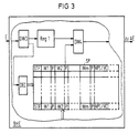
- FIG. 3 shows a possible structure of the previously mentioned treatment facilities BHE. Only those circuit parts are specified which are necessary for understanding the present invention.
- a register Reg1 is connected to the respective input transmission line, which is designated E in FIG. 3, via a data switch DW3.
- the message signal bits of a message cell transmitted via the input transmission line are recorded in this register.
- the cell header associated with the respective message cell is fed to an address decoder DEC via the data switch DW3.
- Corresponding control of the data switch can take place, for example, by means of a comparator arrangement connected upstream of this data switch, which monitors the occurrence of a bit combination (start flag) indicating the beginning of a cell header.
- the address decoder DEC decodes the information contained in a cell header in the form of a virtual channel number VCI and designates the respective virtual connection and provides corresponding output signals. These are fed to a memory SP as address signals.
- the memory has a separate memory cell for each of the virtual connections possible on the associated input transmission line. These memory cells can be controlled in accordance with the virtual channel numbers VCI decoded by the address decoder DEC. In each of these memory cells, with a virtual connection set up, As shown schematically in FIG.
- a cell header defined, for example, according to CCITT recommendation I.361 is stored, which, among other things, contains a bit pattern STF (start flag) indicating the beginning of a cell header, one of the number of coupling stages to be run through in the ATM switching device contains a corresponding number of route information and a virtual channel number VCI defined for the respective virtual connection on the output transmission line in question of the ATM switching device (FIG. 1).
- STF start flag
- VCI virtual channel number
- the information just mentioned and stored in the memory SP is also entered into the memory cell in question by a control device (not shown) in the course of establishing the respective virtual connection.
- the cell header stored in this memory cell is read out and fed to a first input of a data switch DW4.
- the output of the aforementioned Reg1 register is connected to a second input of this data switch.
- This data switch is activated, for example, by a counter (not shown) in such a way that first a cell header read out of the memory SP and then the message signal bits stored in the register Reg1 appear serially at the output of the treatment device BHE shown in FIG.
- FIG. 4 shows a possible structure of the device PR for the shifting of bit groups, which has already been explained with reference to FIG. 2.
- This device then has a first register arrangement RAN1, which has a number of register cells R1 to Rn corresponding to the number of bit groups contained in a cell header.
- These register cells can be controlled, for example, by a counter arrangement such that the bit groups belonging to a cell header and transmitted via the data switch DW1 (FIG. 2) can be written into them one after the other.
- Each of these bit groups corresponds to one of the details entered in a memory cell of the memory SP shown in FIG. 3.
- the first bit group thus represents the bit group STF which indicates the beginning of a cell header.
- the following bit groups each contain one of the path information W1 to Wm including the security information P (parity bit) attached to them.
- the register arrangement RAN 1 is followed by a corresponding register arrangement RAN2 with register cells R1 to Rn.
- the two register arrangements are connected to one another in such a way that the contents of the register cells R1 and Rm + 2 to Rn of the register arrangement RAN1 can be transferred to the register cells R1 and Rm + 2 to Rn of the register arrangement RAN2.
- the remaining register cells R2 to Rm + 1 of the two register arrangements are coupled to one another such that the contents of the register cells R3 to Rm + 1 of the register arrangement RAN1 can be entered into the register cells R2 to Rm of the register arrangement RAN2 are.
- the content of the register cell R2 of the register arrangement RAN1 is transferred to the register cell Rm + 1 of the register arrangement RAN2, the parity bit P attached to the respective route information, here the route information W1, being inverted with the aid of an inverter INV before this transfer.
- a modified cell header is then available in the register arrangement RAN2, in which the route information originally at the first position of the route information, here W1, including the associated parity bit, is shifted to the end of the route information block with simultaneous inversion of the parity bit.
- This modified cell header is then forwarded to the data switch DW2 (FIG. 2) in the manner specified above.
- the route information stored in the register cell R2 of the register arrangement RAN1, i. H. in the present case, the route information W1 is also provided separately in order to be able to forward a message cell with a modified cell header that has just been taken into the respective evaluation device (FIG. 2) in the manner specified above.
- the aforementioned parity checking device PC (FIG. 2) can be activated by the device PR (FIG. 4) for evaluating the first path information occurring in a cell header by activating the register cell R2 of the register arrangement RAN1 for the adoption of a route information emits a corresponding control signal to the parity checking device.
Landscapes
- Engineering & Computer Science (AREA)
- Computer Networks & Wireless Communication (AREA)
- Signal Processing (AREA)
- Computer Security & Cryptography (AREA)
- Data Exchanges In Wide-Area Networks (AREA)
Claims (3)
- Procédé pour la réception et la retransmission de cellules d'information, transmises selon un mode de transfert asynchrone, par un dispositif de commutation ATM (VE), possédant un dispositif de couplage à rebroussement (KS1, KS2) à plusieurs étages, selon lequel, à l'intérieur du dispositif de commutation ATM, un bloc d'informations d'acheminement comportant un nombre d'informations d'acheminement, qui correspond au nombre des étages de couplage devant être traversés, est inséré en avant de chacune des cellules d'information et l'information d'acheminement, qui est précisément évaluée par l'un des étages de couplage pour la retransmission d'une cellule d'information, est ensuite décalée à la fin du bloc respectif d'informations d'acheminement, caractérisé par le fait
qu'une information particulière de sécurité est adjointe à chacune des informations d'acheminement d'un bloc d'informations d'acheminement, que l'information associée de sécurité est faussée avec le décalage d'une information d'acheminement à l'extrémité du bloc respectif d'informations d'acheminement, et
qu'une cellule d'information est retransmise par l'intermédiaire d'un étage de couplage uniquement lorsque l'information d'acheminement, devant être évaluée à cet effet, est identifiée comme étant sans erreur sur la base de l'information de sécurité adjointe. - Procédé suivant la revendication 1, caractérisé par le fait
qu'un bit de parité est adjoint respectivement, en tant qu'information de sécurité, aux informations d'acheminement, et
que le bit de parité associé est inversé avec le décalage d'une information d'acheminement à la fin du bloc respectif d'informations d'acheminement. - Montage pour la réception et la retransmission de cellules d'informations transmises selon un mode de transfert asynchrone au moyen d'un dispositif de commutation ATM (VE) possédant un étage de couplage à rebroussement (KS1, KS2) à plusieurs étages, et dans lequel un bloc d'informations d'acheminement, possédant un nombre d'informations d'acheminement qui correspond au nombre des étages de couplage devant être inversés, est inséré en avant de chacune des cellules d'informations, qui sont reçues par l'intermédiaire des lignes d'entrée du dispositif de commutation ATM, au moyen d'un dispositif de traitement (BHE) associé à la ligne respective d'entrée, et dans lequel à des lignes d'entrée d'un étage de couplage est associé respectivement un dispositif d'évaluation (AE), qui décale ensuite l'information d'acheminement précisément évaluée pour la retransmission d'une cellule d'informations par l'intermédiaire de l'étage de couplage respectif, à la fin du bloc respectif d'informations d'acheminement, caractérisé par le fait
que les dispositifs de traitement (BHE) et les dispositifs d'évaluation (AE) sont agencés respectivement de telle sorte
que les dispositifs de traitement (BHE) adjoignent une formation particulière de sécurité respectivement à chacune des informations d'acheminement d'un bloc d'informations d'acheminement,
que les dispositifs d'évaluation (AE) faussent l'information associée de sécurité, respectivement lors du décalage d'une information d'acheminement à la fin d'un bloc d'informations d'acheminement, et
que les dispositifs d'évaluation (AE) retransmettent respectivement une cellule d'informations par l'intermédiaire de l'étage de couplage associé (KS1,KS2), uniquement lorsque l'information d'acheminement, devant être évaluée à cet effet, est reconnue comme étant exempte d'erreurs, sur la base de l'information de sécurité adjointe.
Applications Claiming Priority (2)
| Application Number | Priority Date | Filing Date | Title |
|---|---|---|---|
| EP90115417 | 1990-08-10 | ||
| EP90115417 | 1990-08-10 |
Publications (2)
| Publication Number | Publication Date |
|---|---|
| EP0470341A1 EP0470341A1 (fr) | 1992-02-12 |
| EP0470341B1 true EP0470341B1 (fr) | 1995-09-20 |
Family
ID=8204319
Family Applications (1)
| Application Number | Title | Priority Date | Filing Date |
|---|---|---|---|
| EP91109315A Expired - Lifetime EP0470341B1 (fr) | 1990-08-10 | 1991-06-06 | Méthode et agencement de commutation pour la réception et la transmission de cellules d'information transmises selon le mode de transfert asynchrone dans un dispositif de commutation ATM |
Country Status (6)
| Country | Link |
|---|---|
| US (1) | US5153920A (fr) |
| EP (1) | EP0470341B1 (fr) |
| JP (1) | JPH04234247A (fr) |
| AT (1) | ATE128300T1 (fr) |
| CA (1) | CA2048708A1 (fr) |
| DE (1) | DE59106514D1 (fr) |
Families Citing this family (16)
| Publication number | Priority date | Publication date | Assignee | Title |
|---|---|---|---|---|
| WO1993026109A1 (fr) * | 1992-06-17 | 1993-12-23 | The Trustees Of The University Of Pennsylvania | Appareil assurant le support cryptographique dans un reseau |
| DE4331579C2 (de) * | 1993-09-16 | 1995-07-06 | Siemens Ag | Verfahren zum Übertragen von Nachrichtenzellen über redundante virtuelle Pfadpaare eines ATM-Kommunikationsnetzes |
| US5446726A (en) * | 1993-10-20 | 1995-08-29 | Lsi Logic Corporation | Error detection and correction apparatus for an asynchronous transfer mode (ATM) network device |
| US5708659A (en) * | 1993-10-20 | 1998-01-13 | Lsi Logic Corporation | Method for hashing in a packet network switching system |
| US5802287A (en) * | 1993-10-20 | 1998-09-01 | Lsi Logic Corporation | Single chip universal protocol multi-function ATM network interface |
| US5606552A (en) * | 1994-10-17 | 1997-02-25 | Lucent Technologies Inc. | Broadband adaptation processing |
| US5936967A (en) * | 1994-10-17 | 1999-08-10 | Lucent Technologies, Inc. | Multi-channel broadband adaptation processing |
| US5841772A (en) * | 1996-03-07 | 1998-11-24 | Lsi Logic Corporation | ATM communication system interconnect/termination unit |
| US5848068A (en) * | 1996-03-07 | 1998-12-08 | Lsi Logic Corporation | ATM communication system interconnect/termination unit |
| US5982749A (en) * | 1996-03-07 | 1999-11-09 | Lsi Logic Corporation | ATM communication system interconnect/termination unit |
| US6535512B1 (en) | 1996-03-07 | 2003-03-18 | Lsi Logic Corporation | ATM communication system interconnect/termination unit |
| US6373846B1 (en) | 1996-03-07 | 2002-04-16 | Lsi Logic Corporation | Single chip networking device with enhanced memory access co-processor |
| US5920561A (en) * | 1996-03-07 | 1999-07-06 | Lsi Logic Corporation | ATM communication system interconnect/termination unit |
| US5831980A (en) * | 1996-09-13 | 1998-11-03 | Lsi Logic Corporation | Shared memory fabric architecture for very high speed ATM switches |
| US5959993A (en) * | 1996-09-13 | 1999-09-28 | Lsi Logic Corporation | Scheduler design for ATM switches, and its implementation in a distributed shared memory architecture |
| US6601217B1 (en) * | 2000-04-13 | 2003-07-29 | Sun Microsystems, Inc. | System and method for error correction in an electronic communication |
Family Cites Families (5)
| Publication number | Priority date | Publication date | Assignee | Title |
|---|---|---|---|---|
| CA1265227A (fr) * | 1985-07-08 | 1990-01-30 | Reginhard Pospischil | Methode pour surveiller et controler le trafic dans les reseaux de transmission numeriques |
| US4794589A (en) * | 1986-09-16 | 1988-12-27 | Gte Communication Systems Corporation | Asynchronous packet manage |
| FR2631183B1 (fr) * | 1988-05-06 | 1991-02-22 | Compex | Procede et dispositif de transmission asynchrone de donnees par paquets |
| US4932020A (en) * | 1988-11-14 | 1990-06-05 | At&T Bell Laboratories | Packet switching arrangement including packet retransmission |
| JP2860661B2 (ja) * | 1989-03-14 | 1999-02-24 | 国際電信電話 株式会社 | Atm交換機 |
-
1991
- 1991-06-06 EP EP91109315A patent/EP0470341B1/fr not_active Expired - Lifetime
- 1991-06-06 DE DE59106514T patent/DE59106514D1/de not_active Expired - Fee Related
- 1991-06-06 AT AT91109315T patent/ATE128300T1/de not_active IP Right Cessation
- 1991-07-31 US US07/738,358 patent/US5153920A/en not_active Expired - Fee Related
- 1991-08-08 JP JP3224843A patent/JPH04234247A/ja not_active Withdrawn
- 1991-08-08 CA CA002048708A patent/CA2048708A1/fr not_active Abandoned
Also Published As
| Publication number | Publication date |
|---|---|
| JPH04234247A (ja) | 1992-08-21 |
| EP0470341A1 (fr) | 1992-02-12 |
| US5153920A (en) | 1992-10-06 |
| CA2048708A1 (fr) | 1992-02-11 |
| ATE128300T1 (de) | 1995-10-15 |
| DE59106514D1 (de) | 1995-10-26 |
Similar Documents
| Publication | Publication Date | Title |
|---|---|---|
| EP0384936B1 (fr) | Procédé et dispositif pour transmettre des paquets d'information provenant de lignes d'entrée via un dispositif à communication de paquets | |
| DE69120166T2 (de) | ATM-Vermittlungsschaltung | |
| DE69231264T2 (de) | ATM-Zellenfehlerverarbeitungssystem | |
| DE68923951T2 (de) | Hochgeschwindigkeits-Kombinierschalter mit Einzelfifo. | |
| DE69330833T2 (de) | Stellenidentifizierung in einem Kommunikationssignalisierungsnetz | |
| EP0470341A1 (fr) | Méthode et agencement de commutation pour la réception et la transmission de cellules d'information transmises selon le mode de transfert asynchrone dans un dispositif de commutation ATM | |
| DE69025143T2 (de) | Fehlertolerante Verbindungsnetze | |
| EP0453607B1 (fr) | Méthode et dispositif pour réduire la perte de paquets d'information, transmis par un commutateur de paquets | |
| DE4432061C1 (de) | Paketübertragungssystem | |
| EP0584398A1 (fr) | Procédé et circuit pour transmettre des cellules d'information dans un réseau ATM | |
| EP0762694A1 (fr) | Réseau local à Mode de Transfert Asynchrome (ATM) avec au moins deux systèmes en anneau | |
| DE4331579A1 (de) | Verfahren zum Übertragen von Nachrichtenzellen über redundante virtuelle Pfadpaare eines ATM-Kommunikationsnetzes | |
| DE3111447A1 (de) | Anzeigeschaltung fuer speicherschreibfehler | |
| EP0219917B1 (fr) | Dispositif de commutation avec correction de fautes | |
| DE2644733A1 (de) | Verfahren und vorrichtung zum direkten ueberpruefen des fehlerfreien betriebs von speichern bei der sequentiellen datenverarbeitung | |
| EP0566961A2 (fr) | Procédé et circuit pour faire respecter le débit de transmission préaccordé dans un dispositif de commutation ATM | |
| DE69221325T2 (de) | Filteranordnung und Verfahren zum Zusammenfügen von ATM-Vermittlungsebenen für ATM-Vermittlungen | |
| DE69326378T2 (de) | Steuerung des Austauschens von Datenpaketen in einem Netzwerk | |
| EP0576856A2 (fr) | Procédé et circuit pour la transmission d'un flux ATM continu de bits | |
| EP0868053B1 (fr) | Système redondant de transmission avec l'arrêt d'une voie défectueuse de transmission | |
| DE3613773C2 (fr) | ||
| DE4121481C1 (fr) | ||
| DE2538802C2 (de) | Schaltung zum Nachweis von Fehlern unter den aus Informations- und Prüfbits erzeugten, einen fehlerhaften Speicherort angebenden Bits | |
| DE1946365A1 (de) | Einrichtung zum Erkennen oder Korrigieren von einzelnen Blockfehlern | |
| EP0410270B1 (fr) | Procédé d'utilisation d'une interface fiable de transmission de signaux |
Legal Events
| Date | Code | Title | Description |
|---|---|---|---|
| PUAI | Public reference made under article 153(3) epc to a published international application that has entered the european phase |
Free format text: ORIGINAL CODE: 0009012 |
|
| AK | Designated contracting states |
Kind code of ref document: A1 Designated state(s): AT BE CH DE FR GB IT LI NL SE |
|
| 17P | Request for examination filed |
Effective date: 19920807 |
|
| 17Q | First examination report despatched |
Effective date: 19940511 |
|
| GRAA | (expected) grant |
Free format text: ORIGINAL CODE: 0009210 |
|
| AK | Designated contracting states |
Kind code of ref document: B1 Designated state(s): AT BE CH DE FR GB IT LI NL SE |
|
| REF | Corresponds to: |
Ref document number: 128300 Country of ref document: AT Date of ref document: 19951015 Kind code of ref document: T |
|
| REF | Corresponds to: |
Ref document number: 59106514 Country of ref document: DE Date of ref document: 19951026 |
|
| REG | Reference to a national code |
Ref country code: CH Ref legal event code: PFA Free format text: SIEMENS AKTIENGESELLSCHAFT BERLIN UND MUENCHEN TRANSFER- SIEMENS AKTIENGESELLSCHAFT |
|
| ITF | It: translation for a ep patent filed | ||
| GBT | Gb: translation of ep patent filed (gb section 77(6)(a)/1977) |
Effective date: 19951127 |
|
| ET | Fr: translation filed | ||
| PLBE | No opposition filed within time limit |
Free format text: ORIGINAL CODE: 0009261 |
|
| STAA | Information on the status of an ep patent application or granted ep patent |
Free format text: STATUS: NO OPPOSITION FILED WITHIN TIME LIMIT |
|
| 26N | No opposition filed | ||
| PGFP | Annual fee paid to national office [announced via postgrant information from national office to epo] |
Ref country code: GB Payment date: 19970521 Year of fee payment: 7 |
|
| PGFP | Annual fee paid to national office [announced via postgrant information from national office to epo] |
Ref country code: AT Payment date: 19970602 Year of fee payment: 7 |
|
| PGFP | Annual fee paid to national office [announced via postgrant information from national office to epo] |
Ref country code: BE Payment date: 19970609 Year of fee payment: 7 |
|
| PGFP | Annual fee paid to national office [announced via postgrant information from national office to epo] |
Ref country code: SE Payment date: 19970612 Year of fee payment: 7 |
|
| PGFP | Annual fee paid to national office [announced via postgrant information from national office to epo] |
Ref country code: NL Payment date: 19970619 Year of fee payment: 7 |
|
| PGFP | Annual fee paid to national office [announced via postgrant information from national office to epo] |
Ref country code: FR Payment date: 19970626 Year of fee payment: 7 |
|
| PGFP | Annual fee paid to national office [announced via postgrant information from national office to epo] |
Ref country code: DE Payment date: 19970820 Year of fee payment: 7 |
|
| PGFP | Annual fee paid to national office [announced via postgrant information from national office to epo] |
Ref country code: CH Payment date: 19970912 Year of fee payment: 7 |
|
| PG25 | Lapsed in a contracting state [announced via postgrant information from national office to epo] |
Ref country code: GB Free format text: LAPSE BECAUSE OF NON-PAYMENT OF DUE FEES Effective date: 19980606 Ref country code: AT Free format text: LAPSE BECAUSE OF NON-PAYMENT OF DUE FEES Effective date: 19980606 |
|
| PG25 | Lapsed in a contracting state [announced via postgrant information from national office to epo] |
Ref country code: SE Free format text: LAPSE BECAUSE OF NON-PAYMENT OF DUE FEES Effective date: 19980607 |
|
| PG25 | Lapsed in a contracting state [announced via postgrant information from national office to epo] |
Ref country code: LI Free format text: LAPSE BECAUSE OF NON-PAYMENT OF DUE FEES Effective date: 19980630 Ref country code: CH Free format text: LAPSE BECAUSE OF NON-PAYMENT OF DUE FEES Effective date: 19980630 Ref country code: BE Free format text: LAPSE BECAUSE OF NON-PAYMENT OF DUE FEES Effective date: 19980630 |
|
| BERE | Be: lapsed |
Owner name: SIEMENS A.G. Effective date: 19980630 |
|
| PG25 | Lapsed in a contracting state [announced via postgrant information from national office to epo] |
Ref country code: NL Free format text: LAPSE BECAUSE OF NON-PAYMENT OF DUE FEES Effective date: 19990101 |
|
| GBPC | Gb: european patent ceased through non-payment of renewal fee |
Effective date: 19980606 |
|
| REG | Reference to a national code |
Ref country code: CH Ref legal event code: PL |
|
| PG25 | Lapsed in a contracting state [announced via postgrant information from national office to epo] |
Ref country code: FR Free format text: LAPSE BECAUSE OF NON-PAYMENT OF DUE FEES Effective date: 19990226 |
|
| EUG | Se: european patent has lapsed |
Ref document number: 91109315.1 |
|
| NLV4 | Nl: lapsed or anulled due to non-payment of the annual fee |
Effective date: 19990101 |
|
| PG25 | Lapsed in a contracting state [announced via postgrant information from national office to epo] |
Ref country code: DE Free format text: LAPSE BECAUSE OF NON-PAYMENT OF DUE FEES Effective date: 19990401 |
|
| REG | Reference to a national code |
Ref country code: FR Ref legal event code: ST |
|
| PG25 | Lapsed in a contracting state [announced via postgrant information from national office to epo] |
Ref country code: IT Free format text: LAPSE BECAUSE OF NON-PAYMENT OF DUE FEES;WARNING: LAPSES OF ITALIAN PATENTS WITH EFFECTIVE DATE BEFORE 2007 MAY HAVE OCCURRED AT ANY TIME BEFORE 2007. THE CORRECT EFFECTIVE DATE MAY BE DIFFERENT FROM THE ONE RECORDED. Effective date: 20050606 |