EP0470850A2 - Schaltkreis zum Schalten eines Hochspannungsdünnfilmtransistors - Google Patents
Schaltkreis zum Schalten eines Hochspannungsdünnfilmtransistors Download PDFInfo
- Publication number
- EP0470850A2 EP0470850A2 EP91307321A EP91307321A EP0470850A2 EP 0470850 A2 EP0470850 A2 EP 0470850A2 EP 91307321 A EP91307321 A EP 91307321A EP 91307321 A EP91307321 A EP 91307321A EP 0470850 A2 EP0470850 A2 EP 0470850A2
- Authority
- EP
- European Patent Office
- Prior art keywords
- thin film
- transistor
- film transistor
- high voltage
- low voltage
- Prior art date
- Legal status (The legal status is an assumption and is not a legal conclusion. Google has not performed a legal analysis and makes no representation as to the accuracy of the status listed.)
- Granted
Links
Images



Classifications
-
- H—ELECTRICITY
- H03—ELECTRONIC CIRCUITRY
- H03K—PULSE TECHNIQUE
- H03K17/00—Electronic switching or gating, i.e. not by contact-making and –breaking
- H03K17/51—Electronic switching or gating, i.e. not by contact-making and –breaking characterised by the components used
- H03K17/56—Electronic switching or gating, i.e. not by contact-making and –breaking characterised by the components used by the use, as active elements, of semiconductor devices
- H03K17/687—Electronic switching or gating, i.e. not by contact-making and –breaking characterised by the components used by the use, as active elements, of semiconductor devices the devices being field-effect transistors
- H03K17/693—Switching arrangements with several input- or output-terminals, e.g. multiplexers, distributors
-
- H—ELECTRICITY
- H03—ELECTRONIC CIRCUITRY
- H03K—PULSE TECHNIQUE
- H03K17/00—Electronic switching or gating, i.e. not by contact-making and –breaking
- H03K17/10—Modifications for increasing the maximum permissible switched voltage
- H03K17/102—Modifications for increasing the maximum permissible switched voltage in field-effect transistor switches
-
- H—ELECTRICITY
- H03—ELECTRONIC CIRCUITRY
- H03K—PULSE TECHNIQUE
- H03K17/00—Electronic switching or gating, i.e. not by contact-making and –breaking
- H03K17/51—Electronic switching or gating, i.e. not by contact-making and –breaking characterised by the components used
- H03K17/56—Electronic switching or gating, i.e. not by contact-making and –breaking characterised by the components used by the use, as active elements, of semiconductor devices
- H03K17/687—Electronic switching or gating, i.e. not by contact-making and –breaking characterised by the components used by the use, as active elements, of semiconductor devices the devices being field-effect transistors
- H03K17/6871—Electronic switching or gating, i.e. not by contact-making and –breaking characterised by the components used by the use, as active elements, of semiconductor devices the devices being field-effect transistors the output circuit comprising more than one controlled field-effect transistor
Definitions
- the present invention relates to a circuit for switching an amorphous silicon high voltage thin film transistor (HVTFT) substantially over its full range in an efficient and stable manner.
- HVTFT high voltage thin film transistor
- FIG. 1 An example of a typical high voltage circuit application subject to this problem is the resistive inverter circuit used in the electrographic writing head 10 schematically illustrated in Figure 1.
- the writing head 10 comprises a linear array of several thousand styli 12 for generating sequential raster lines of information by means of high voltage electrical discharges across a minute air gap to a conductive electrode.
- a multiplexing scheme is used wherein the charge on each stylus is controlled by a low voltage thin film pass transistor (LVTFT) 14 which selectively charges and discharges the gate of a thin film high voltage transistor 16 for switching the HVTFT.
- LVTFT low voltage thin film pass transistor
- HVTFT 16 The drain electrode 18 of HVTFT 16 is connected to high voltage bus 20 (maintained at about 450 volts relative to ground) via load resistor 22, and its source electrode 24 is connected to ground bus 26.
- Data signals, from data lines 28, on the order of 20 volts (ON) and 0 volts (OFF) will be imposed upon the gate electrode of the HVTFT when the address line 30 switches the gate of LVTFT 14 between about 24 volts (ON) and 0 volts (OFF) during a "gate time" of about 15 to 25 ⁇ sec, i.e. the time it takes for the gate of the HVTFT to reach its desired potential.
- the switching efficiency is poor and the drain electrode (and the stylus) will achieve only about 200 to 250 volts rather than the intended 450 volts because the HVTFT doesn't turn fully OFF and the stylus will write gray rather than white (non-write).
- a known solution to the switching efficiency problem caused by gate-to-drain parasitic capacitance is the use of a cascode circuit wherein the switching transistor is connected in series with the switched transistor and the gate of the switched transistor is biased to a fixed potential.
- this solution when this solution is applied to an amorphous silicon HVTFT (switched transistor) it triggers an instability in the device which shifts the I DS vs. V DS characteristic curve to the right over time. This instability is characterized by a parameter V X , and the resulting curve is said to be V X shifted.
- curve A represents an initial (unstressed) condition and curve B represents a V X shifted condition.
- V TH shift Another problem exhibited by amorphous silicon transistors is a threshold voltage V TH shift which occurs during normal usage when the device is maintained in its ON state for an extended period of time.
- V TH of the HVTFT increases, the normal 0 volt bias on the gate for maintaining the OFF state of the device falls far below V TH and induces the V X instability.
- the present invention provides a cascode circuit for switching a high voltage thin film transistor substantially over its entire high voltage range, comprising a low voltage thin film transistor connected in series with said high voltage thin film transistor, each of said transistors including a source electrode, a drain electrode and a gate electrode, said drain electrode of said high voltage transistor being coupled to a source of high potential, said source electrode of said high voltage transistor being coupled to said drain of said low voltage transistor and said source electrode of said low voltage transistor being coupled to a source of reference potential, characterised by a thin film space charge limited current shunt connected in parallel with said low voltage transistor between said source electrode and said drain electrode of said low voltage transistor.
- a cascode circuit for switching a high voltage thin film transistor substantially over its entire high voltage range comprising a low voltage thin film transistor connected in series with said high voltage thin film transistor, said transistors being coupled between a source of high potential and a source of reference potential, characterised in that said low voltage thin film transistor is connected in parallel with a thin film space charge limited current shunt together defining a leaky low voltage thin film transistor.
- the present invention may be carried out, in one form, by providing a cascode circuit for switching a high voltage thin film transistor substantially over its entire high voltage range, comprising a leaky low voltage thin film transistor connected in series with the high voltage thin film transistor, the transistors being connected between a source of high potential and a source of reference potential.
- the leaky low voltage thin film transistor comprises a space charge limited current shunt connected in parallel with a low voltage transistor.
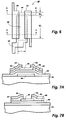
- the cascode circuit illustrated in Figure 5 solves the switching and reliability problems. It comprises a low voltage thin film pass transistor 36 and a novel low voltage thin film switching transistor 38 for switching the source electrode potential of the HVTFT in order to turn the device ON and OFF while maintaining a fixed potential on the gate electrode 30 of the HVTFT.
- the floating gate of the switching LVTFT is completely isolated from the large voltage swings of the HVTFT drain, therefore, the switching efficiency problem of that device is eliminated.
- the novel low voltage thin film switching transistor 38 is provided with a space charge limited shunt 40 in parallel with the switching transistor 38 for insuring a leakage path to the reference potential in order to prevent the V X shift in the HVTFT, as will become apparent hereinafter.
- the novel shunted LVTFT 38 is basically a standard amorphous silicon LVTFT comprising a substrate 42, a conductive gate electrode layer 44, a gate dielectric layer 46, a substantially intrinsic amorphous silicon charge transport layer 48, doped (n+) amorphous silicon source and drain electrodes 50 and 52, conductive source and drain contacts 54 and 56, and top dielectric layer 58.
- the amorphous silicon layer 48 and the source and drain electrodes 50 and 52 extend beyond the gate electrode 44 in the region of section B-B so that that portion of the amorphous silicon charge transport island is ungated and has a current path parallel to the gated current path through the transistor. Whenever there is a potential drop between the source electrode and the drain electrode, space charge limited current will flow thereacross in the ungated region.
- the novel shunted thin film transistor is easily fabricated, requiring no more processing steps than necessary for fabrication of the conventional transistor.
- the amorphous silicon charge transport island and the source and drain electrodes need merely to be extended beyond the end of the gate electrode.
- a matching leakage current (10 9.5 amps) through the HVTFT in its OFF state will result in a gate voltage (V GS ) of about -.8 volts (see Figure 3) or about 2.3 volts below the identified HVTFT threshold voltage (V TH ) of about 1.5 volts.
- V TH is typically about 1.5 volts.
- V TH could rise by 2, 3 or more volts (2 volts illustrated in Figure 4).
- the cascode circuit solution is well known for overcoming the switching efficiency problem caused by parasitic capacitance, its implementation in amorphous silicon raises the specter of the V X shift phenomenon. It has been found that the stability of the HVTFT may be increased with the introduction of the novel LVTFT 38 having a parallel space charge limited shunt 40.
- the novel leaky LVTFT not only prevents the V X shift from occurring in the HVTFT by avoiding a hard OFF state which puts the device into an unstable condition, but actually makes the circuit more stable under all conditions.
Landscapes
- Thin Film Transistor (AREA)
- Electronic Switches (AREA)
Applications Claiming Priority (2)
| Application Number | Priority Date | Filing Date | Title |
|---|---|---|---|
| US07/565,767 US5073723A (en) | 1990-08-10 | 1990-08-10 | Space charge current limited shunt in a cascode circuit for hvtft devices |
| US565767 | 1990-08-10 |
Publications (3)
| Publication Number | Publication Date |
|---|---|
| EP0470850A2 true EP0470850A2 (de) | 1992-02-12 |
| EP0470850A3 EP0470850A3 (en) | 1992-06-03 |
| EP0470850B1 EP0470850B1 (de) | 1997-04-02 |
Family
ID=24260004
Family Applications (1)
| Application Number | Title | Priority Date | Filing Date |
|---|---|---|---|
| EP91307321A Expired - Lifetime EP0470850B1 (de) | 1990-08-10 | 1991-08-09 | Schaltkreis zum Schalten eines Hochspannungsdünnfilmtransistors |
Country Status (4)
| Country | Link |
|---|---|
| US (1) | US5073723A (de) |
| EP (1) | EP0470850B1 (de) |
| JP (1) | JP2728808B2 (de) |
| DE (1) | DE69125434T2 (de) |
Cited By (2)
| Publication number | Priority date | Publication date | Assignee | Title |
|---|---|---|---|---|
| WO1994013049A1 (en) * | 1992-11-30 | 1994-06-09 | Nokia Telecommunications Oy | Arrangement in a current limited circuit for transferring overload power |
| EP2764538A4 (de) * | 2011-10-07 | 2015-05-27 | Transphorm Inc | Elektronische hochleistungshalbleiter-bauteile mit erhöhter zuverlässigkeit |
Families Citing this family (8)
| Publication number | Priority date | Publication date | Assignee | Title |
|---|---|---|---|---|
| JP2653099B2 (ja) * | 1988-05-17 | 1997-09-10 | セイコーエプソン株式会社 | アクティブマトリクスパネル,投写型表示装置及びビューファインダー |
| US5274279A (en) * | 1988-05-17 | 1993-12-28 | Seiko Epson Corporation | Thin film CMOS inverter |
| US5166960A (en) * | 1992-04-20 | 1992-11-24 | Xerox Corporation | Parallel multi-phased a-Si shift register for fast addressing of an a-Si array |
| US5237346A (en) * | 1992-04-20 | 1993-08-17 | Xerox Corporation | Integrated thin film transistor electrographic writing head |
| US6022770A (en) * | 1998-03-24 | 2000-02-08 | International Business Machines Corporation | NVRAM utilizing high voltage TFT device and method for making the same |
| EP2784816A1 (de) * | 2013-03-28 | 2014-10-01 | Nxp B.V. | Kaskodenhalbleiterbauelement |
| CN110661417B (zh) * | 2018-06-29 | 2021-07-27 | 中国科学院微电子研究所 | 一种电压传输电路及相关电路结构 |
| US10848153B2 (en) * | 2018-11-30 | 2020-11-24 | Micron Technology, Inc. | Leakage current reduction in electronic devices |
Family Cites Families (10)
| Publication number | Priority date | Publication date | Assignee | Title |
|---|---|---|---|---|
| WO1981001924A1 (fr) * | 1979-12-28 | 1981-07-09 | Int Rectifier Corp Jp Ltd | Configuration de circuit de transistor a effet de champ |
| FR2524714B1 (fr) * | 1982-04-01 | 1986-05-02 | Suwa Seikosha Kk | Transistor a couche mince |
| US4862237A (en) * | 1983-01-10 | 1989-08-29 | Seiko Epson Corporation | Solid state image sensor |
| US4752814A (en) * | 1984-03-12 | 1988-06-21 | Xerox Corporation | High voltage thin film transistor |
| US4719481A (en) * | 1984-12-04 | 1988-01-12 | Xerox Corporation | Electrographic ion writing head driver system |
| FR2593632B1 (fr) * | 1986-01-27 | 1988-03-18 | Maurice Francois | Ecran d'affichage a matrice active et procedes de realisation de cet ecran |
| US5032883A (en) * | 1987-09-09 | 1991-07-16 | Casio Computer Co., Ltd. | Thin film transistor and method of manufacturing the same |
| US4960719A (en) * | 1988-02-04 | 1990-10-02 | Seikosha Co., Ltd. | Method for producing amorphous silicon thin film transistor array substrate |
| JPH02182024A (ja) * | 1989-01-06 | 1990-07-16 | Nec Corp | 電界効果トランジスタ集積回路 |
| US4998146A (en) * | 1989-05-24 | 1991-03-05 | Xerox Corporation | High voltage thin film transistor |
-
1990
- 1990-08-10 US US07/565,767 patent/US5073723A/en not_active Expired - Lifetime
-
1991
- 1991-08-05 JP JP3195353A patent/JP2728808B2/ja not_active Expired - Fee Related
- 1991-08-09 EP EP91307321A patent/EP0470850B1/de not_active Expired - Lifetime
- 1991-08-09 DE DE69125434T patent/DE69125434T2/de not_active Expired - Fee Related
Cited By (2)
| Publication number | Priority date | Publication date | Assignee | Title |
|---|---|---|---|---|
| WO1994013049A1 (en) * | 1992-11-30 | 1994-06-09 | Nokia Telecommunications Oy | Arrangement in a current limited circuit for transferring overload power |
| EP2764538A4 (de) * | 2011-10-07 | 2015-05-27 | Transphorm Inc | Elektronische hochleistungshalbleiter-bauteile mit erhöhter zuverlässigkeit |
Also Published As
| Publication number | Publication date |
|---|---|
| JPH04234217A (ja) | 1992-08-21 |
| JP2728808B2 (ja) | 1998-03-18 |
| US5073723A (en) | 1991-12-17 |
| DE69125434D1 (de) | 1997-05-07 |
| DE69125434T2 (de) | 1997-08-28 |
| EP0470850B1 (de) | 1997-04-02 |
| EP0470850A3 (en) | 1992-06-03 |
Similar Documents
| Publication | Publication Date | Title |
|---|---|---|
| US4087795A (en) | Memory field effect storage device | |
| EP1355316B1 (de) | Datenspeichergerät sowie Verfahren zum Auffrischen der auf einem solchen Gerät gespeicherten Daten | |
| US5289401A (en) | Analog storage device for artificial neural network system | |
| US6281737B1 (en) | Method and apparatus for reducing parasitic bipolar current in a silicon-on-insulator transistor | |
| US4541073A (en) | Non-volatile flip-flop with a static resetting | |
| EP0616334B1 (de) | Nichtfluechtige halbleiterspeicheranordnung mit isolierter gate-elektrode | |
| EP0470850B1 (de) | Schaltkreis zum Schalten eines Hochspannungsdünnfilmtransistors | |
| KR20020040609A (ko) | 개선된 전압준위변환회로를 가지는 표시장치 | |
| US4443718A (en) | Nonvolatile semiconductor memory with stabilized level shift circuit | |
| JPS62117196A (ja) | 電気的に消去可能なプログラム可能なメモリ・セルとその製法 | |
| JPH0143400B2 (de) | ||
| US4463273A (en) | Electronic circuits and structures employing enhancement and depletion type IGFETs | |
| EP0350879B1 (de) | Ausgangstreiberschaltung für Halbleiter-IC | |
| EP0372087B1 (de) | Befehlschaltung | |
| EP0194091A2 (de) | Programmierbare logische Schaltung mit begrenzten Leserströmen | |
| US4123669A (en) | Logical OR circuit for programmed logic arrays | |
| US7586467B2 (en) | Load drive circuit, integrated circuit, and plasma display | |
| US5105246A (en) | Leaky low voltage thin film transistor | |
| EP0078502B1 (de) | Speicherschaltung | |
| US4506349A (en) | Cross-coupled transistor memory cell for MOS random access memory of reduced power dissipation | |
| EP0157389A2 (de) | Schutzanordnung für einen MOS-Transistor | |
| EP0106942A2 (de) | Steuersystem für eine Plasmaanzeigeeinrichtung | |
| CN1135564C (zh) | 用于高速存储器读操作的总线中点保持电路 | |
| EP0013117B1 (de) | Dynamische logische MOS-Schaltung | |
| JPS6367370B2 (de) |
Legal Events
| Date | Code | Title | Description |
|---|---|---|---|
| PUAI | Public reference made under article 153(3) epc to a published international application that has entered the european phase |
Free format text: ORIGINAL CODE: 0009012 |
|
| AK | Designated contracting states |
Kind code of ref document: A2 Designated state(s): DE FR GB |
|
| PUAL | Search report despatched |
Free format text: ORIGINAL CODE: 0009013 |
|
| AK | Designated contracting states |
Kind code of ref document: A3 Designated state(s): DE FR GB |
|
| 17P | Request for examination filed |
Effective date: 19921202 |
|
| 17Q | First examination report despatched |
Effective date: 19951219 |
|
| GRAG | Despatch of communication of intention to grant |
Free format text: ORIGINAL CODE: EPIDOS AGRA |
|
| GRAH | Despatch of communication of intention to grant a patent |
Free format text: ORIGINAL CODE: EPIDOS IGRA |
|
| GRAH | Despatch of communication of intention to grant a patent |
Free format text: ORIGINAL CODE: EPIDOS IGRA |
|
| GRAA | (expected) grant |
Free format text: ORIGINAL CODE: 0009210 |
|
| AK | Designated contracting states |
Kind code of ref document: B1 Designated state(s): DE FR GB |
|
| REF | Corresponds to: |
Ref document number: 69125434 Country of ref document: DE Date of ref document: 19970507 |
|
| ET | Fr: translation filed | ||
| PLBE | No opposition filed within time limit |
Free format text: ORIGINAL CODE: 0009261 |
|
| STAA | Information on the status of an ep patent application or granted ep patent |
Free format text: STATUS: NO OPPOSITION FILED WITHIN TIME LIMIT |
|
| 26N | No opposition filed | ||
| REG | Reference to a national code |
Ref country code: GB Ref legal event code: IF02 |
|
| REG | Reference to a national code |
Ref country code: GB Ref legal event code: 746 Effective date: 20050512 |
|
| PGFP | Annual fee paid to national office [announced via postgrant information from national office to epo] |
Ref country code: GB Payment date: 20050803 Year of fee payment: 15 |
|
| PGFP | Annual fee paid to national office [announced via postgrant information from national office to epo] |
Ref country code: DE Payment date: 20050804 Year of fee payment: 15 |
|
| PGFP | Annual fee paid to national office [announced via postgrant information from national office to epo] |
Ref country code: FR Payment date: 20050809 Year of fee payment: 15 |
|
| PG25 | Lapsed in a contracting state [announced via postgrant information from national office to epo] |
Ref country code: DE Free format text: LAPSE BECAUSE OF NON-PAYMENT OF DUE FEES Effective date: 20070301 |
|
| GBPC | Gb: european patent ceased through non-payment of renewal fee |
Effective date: 20060809 |
|
| REG | Reference to a national code |
Ref country code: FR Ref legal event code: ST Effective date: 20070430 |
|
| PG25 | Lapsed in a contracting state [announced via postgrant information from national office to epo] |
Ref country code: GB Free format text: LAPSE BECAUSE OF NON-PAYMENT OF DUE FEES Effective date: 20060809 |
|
| PG25 | Lapsed in a contracting state [announced via postgrant information from national office to epo] |
Ref country code: FR Free format text: LAPSE BECAUSE OF NON-PAYMENT OF DUE FEES Effective date: 20060831 |