EP0471380A1 - ATM-Vermittlungsschaltung - Google Patents
ATM-Vermittlungsschaltung Download PDFInfo
- Publication number
- EP0471380A1 EP0471380A1 EP91113792A EP91113792A EP0471380A1 EP 0471380 A1 EP0471380 A1 EP 0471380A1 EP 91113792 A EP91113792 A EP 91113792A EP 91113792 A EP91113792 A EP 91113792A EP 0471380 A1 EP0471380 A1 EP 0471380A1
- Authority
- EP
- European Patent Office
- Prior art keywords
- partial cells
- cell
- partial
- circuits
- cells
- Prior art date
- Legal status (The legal status is an assumption and is not a legal conclusion. Google has not performed a legal analysis and makes no representation as to the accuracy of the status listed.)
- Granted
Links
- 238000000638 solvent extraction Methods 0.000 claims abstract description 35
- 238000012937 correction Methods 0.000 claims abstract description 12
- 238000001514 detection method Methods 0.000 claims description 15
- 238000000034 method Methods 0.000 claims description 4
- 239000000872 buffer Substances 0.000 description 10
- 238000010586 diagram Methods 0.000 description 9
- 238000003780 insertion Methods 0.000 description 8
- 230000037431 insertion Effects 0.000 description 8
- 238000012546 transfer Methods 0.000 description 3
- 238000010276 construction Methods 0.000 description 1
- 125000004122 cyclic group Chemical group 0.000 description 1
- 238000011161 development Methods 0.000 description 1
- 230000000694 effects Effects 0.000 description 1
- 238000004193 electrokinetic chromatography Methods 0.000 description 1
- 238000005516 engineering process Methods 0.000 description 1
- 238000012986 modification Methods 0.000 description 1
- 230000004048 modification Effects 0.000 description 1
- 238000005192 partition Methods 0.000 description 1
- 238000012545 processing Methods 0.000 description 1
- 230000001902 propagating effect Effects 0.000 description 1
Images




Classifications
-
- H—ELECTRICITY
- H04—ELECTRIC COMMUNICATION TECHNIQUE
- H04L—TRANSMISSION OF DIGITAL INFORMATION, e.g. TELEGRAPHIC COMMUNICATION
- H04L12/00—Data switching networks
- H04L12/54—Store-and-forward switching systems
- H04L12/56—Packet switching systems
- H04L12/5601—Transfer mode dependent, e.g. ATM
-
- H—ELECTRICITY
- H04—ELECTRIC COMMUNICATION TECHNIQUE
- H04L—TRANSMISSION OF DIGITAL INFORMATION, e.g. TELEGRAPHIC COMMUNICATION
- H04L1/00—Arrangements for detecting or preventing errors in the information received
- H04L1/004—Arrangements for detecting or preventing errors in the information received by using forward error control
-
- H—ELECTRICITY
- H04—ELECTRIC COMMUNICATION TECHNIQUE
- H04L—TRANSMISSION OF DIGITAL INFORMATION, e.g. TELEGRAPHIC COMMUNICATION
- H04L1/00—Arrangements for detecting or preventing errors in the information received
- H04L1/004—Arrangements for detecting or preventing errors in the information received by using forward error control
- H04L1/0041—Arrangements at the transmitter end
-
- H—ELECTRICITY
- H04—ELECTRIC COMMUNICATION TECHNIQUE
- H04L—TRANSMISSION OF DIGITAL INFORMATION, e.g. TELEGRAPHIC COMMUNICATION
- H04L1/00—Arrangements for detecting or preventing errors in the information received
- H04L1/0078—Avoidance of errors by organising the transmitted data in a format specifically designed to deal with errors, e.g. location
- H04L1/0085—Formatting with cells
-
- H—ELECTRICITY
- H04—ELECTRIC COMMUNICATION TECHNIQUE
- H04L—TRANSMISSION OF DIGITAL INFORMATION, e.g. TELEGRAPHIC COMMUNICATION
- H04L49/00—Packet switching elements
- H04L49/15—Interconnection of switching modules
- H04L49/1515—Non-blocking multistage, e.g. Clos
- H04L49/153—ATM switching fabrics having parallel switch planes
- H04L49/1538—Cell slicing
-
- H—ELECTRICITY
- H04—ELECTRIC COMMUNICATION TECHNIQUE
- H04L—TRANSMISSION OF DIGITAL INFORMATION, e.g. TELEGRAPHIC COMMUNICATION
- H04L49/00—Packet switching elements
- H04L49/15—Interconnection of switching modules
- H04L49/1553—Interconnection of ATM switching modules, e.g. ATM switching fabrics
-
- H—ELECTRICITY
- H04—ELECTRIC COMMUNICATION TECHNIQUE
- H04L—TRANSMISSION OF DIGITAL INFORMATION, e.g. TELEGRAPHIC COMMUNICATION
- H04L49/00—Packet switching elements
- H04L49/25—Routing or path finding in a switch fabric
- H04L49/253—Routing or path finding in a switch fabric using establishment or release of connections between ports
- H04L49/255—Control mechanisms for ATM switching fabrics
-
- H—ELECTRICITY
- H04—ELECTRIC COMMUNICATION TECHNIQUE
- H04L—TRANSMISSION OF DIGITAL INFORMATION, e.g. TELEGRAPHIC COMMUNICATION
- H04L49/00—Packet switching elements
- H04L49/30—Peripheral units, e.g. input or output ports
- H04L49/3081—ATM peripheral units, e.g. policing, insertion or extraction
- H04L49/309—Header conversion, routing tables or routing tags
-
- H—ELECTRICITY
- H04—ELECTRIC COMMUNICATION TECHNIQUE
- H04L—TRANSMISSION OF DIGITAL INFORMATION, e.g. TELEGRAPHIC COMMUNICATION
- H04L12/00—Data switching networks
- H04L12/54—Store-and-forward switching systems
- H04L12/56—Packet switching systems
- H04L12/5601—Transfer mode dependent, e.g. ATM
- H04L2012/5625—Operations, administration and maintenance [OAM]
- H04L2012/5627—Fault tolerance and recovery
-
- H—ELECTRICITY
- H04—ELECTRIC COMMUNICATION TECHNIQUE
- H04L—TRANSMISSION OF DIGITAL INFORMATION, e.g. TELEGRAPHIC COMMUNICATION
- H04L12/00—Data switching networks
- H04L12/54—Store-and-forward switching systems
- H04L12/56—Packet switching systems
- H04L12/5601—Transfer mode dependent, e.g. ATM
- H04L2012/5638—Services, e.g. multimedia, GOS, QOS
- H04L2012/5646—Cell characteristics, e.g. loss, delay, jitter, sequence integrity
- H04L2012/5652—Cell construction, e.g. including header, packetisation, depacketisation, assembly, reassembly
-
- H—ELECTRICITY
- H04—ELECTRIC COMMUNICATION TECHNIQUE
- H04L—TRANSMISSION OF DIGITAL INFORMATION, e.g. TELEGRAPHIC COMMUNICATION
- H04L12/00—Data switching networks
- H04L12/54—Store-and-forward switching systems
- H04L12/56—Packet switching systems
- H04L12/5601—Transfer mode dependent, e.g. ATM
- H04L2012/5678—Traffic aspects, e.g. arbitration, load balancing, smoothing, buffer management
- H04L2012/5681—Buffer or queue management
Definitions
- the present invention relates to an asynchronous transfer mode (ATM) switch in which information switching is accomplished in a unit of cells or to an ATM switch and a method of controlling the same in an ATM cross-connection system.
- ATM asynchronous transfer mode
- each ATM cell is assigned with a routing tag so as to be routed depending on the routing tag.
- an ATM cell is 53 bytes long.
- a routing tag is added thereto such that an ATM cell in the switch includes 54 to 64 bytes.
- the ATM cell has a period or cycle of about 44 cells for each 125 microseconds (us) in a 150 Mb/s operation.
- an ATM switch processing about 2800 cells in each 125 us (equivalent to 150 Mb/s x 64 lines) has a switching capacity of about 10 Gb/s.
- a plurality of unitary switch LSls are arranged in a two-dimensional structure.
- the switching capacity of the unitary ATM switch is restricted by the size of a hardware system of the switch to be mounted in a one-chip LSI and the signal capacity i.e. the maximum number of input/output signals to be processed by the one-chip LSI.
- the unitary switches are required to be configured in a two-dimensional form as described above. However, this is attended with a problem that the hardware size increases in proportion to a square of the switch capacity.
- JP-A-2-2767 (laid-open on Jan. 8, 1990) corresponding to DE-A-3742941 shows a packet switch system having input devices, one provided between a switch and each of inputs, in which the input devices serve to divide packets into sub-packets.
- an ATM switch comprising cell partitioning circuits each for subdividing an ATM cell into N partial cells (N is an integer more than one) and for assigning an identical routing tag to the obtained partial cells and N partial cell switches for respectively routing the N partial cells in an independent fashion based on the routing tag.
- the total switching capacity of the ATM switch is obtained by multiplying the capacity of the unitary partial cell switch by the cell partitioning value of the number of the total partition cells; consequently, there can be configured a unitary ATM switch having a remarkably large capacity by increasing the cell partitioning value.
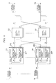
- the configuration of an ATM switch of Fig. 1 includes 2.4 Gb/s incoming highways 1 to 8, cell partitioning circuits 21 to 28, partial cell switches 30 to 37, and 2.4 Gb/s outgoing highways 71 to 78.
- the cell partitioning circuits 21 to 28 respectively include routing tag insertion circuits 210 to 217, 220 to 227, ..., and 280 to 287.
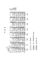
- Each of the 2.4 Gb/s incoming highways 1 to 8 is disposed to receive a 56-byte ATM cell in a format of "40 Mb/s x 64 bits in parallel x 7 rows" as shown in Fig. 2.
- the ATM cell includes an 8-byte cell header and 48-byte cell information field.
- Each of the cell partitioning circuits 21 to 28 subdivids the cell in the form at "40 Mb/s x 64 bits in parallel x 7 rows" into eight portions including eight bits in parallel and assign an identical routing tag thereto, thereby obtaining eight partial cells 150 to 157 as shown in Fig. 3. These partial cells are then sent to the different partial switches respectively associated therewith.
- the routing tag insertion circuit 210 outputs a 0-th partial cell 150 to the partial cell switch 30 and the routing tag insertion circuit 211 supplies a first partial cell 151 to the partial cell switch 31.
- the partial cell switch 30 0-th partial cells are received respectively from the cell partitioning circuits 21 to 28 so as to achieve a switching operation on the received 0-th partial cells based on the routing tags respectively assigned thereto.
- the partial cell switches 31 to 37 conduct switching operations respectively of the first to seventh partial cells. Since the partial cells created from a cell are assigned with an identical routing tag, all partial cell switches 30 to 37 accomplish a similar switching operation when the circuit system operates in the normal state. In consequence, the 2.4 Gb/s outgoing highways 71 to 78 simultaneously receive the respective partial cells constituting the cell.
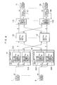
- An ATM switch of Fig. 4 includes 2.4 Gb/s incoming highways 1 to 8, error correcting code (ECC) coder circuits 11 to 18, cell partitioning circuits 21 to 28, partial cell switches 30 to 39, ECC decoder circuits 51 to 58, error counters 61 to 68, and 2.4 Gb/s outgoing highways 71 to 78.
- the cell partitioning circuits 21 to 28 comprise routing tag insertion circuits 210 to 219, 220 to 229, ..., 280 to 289, respectively.
- the operation of the second embodiment will now be described.
- the ECC coder circuits 11 to 18 simultaneously receive 64 bits to generate an ECC based on a 1-byte error correcting Read-Solomon code on a Galois field GF(2 8 ).
- the ECC is a shortened Read-Solomon code created from a generator polynomial where, the code length is ten bytes, the information length is eight bytes, the check symbol length is two bytes, the minimum distance is three bytes, and a is a primitive element of the Galois field GF-(2 8 ).
- Each of the ECC coder circuits 11 to 18 accomplishes a computation by the generator polynomial to produce a two-byte check symbol; moreover, the cell received from the pertinent highway is transformed into a format of "40 Mb/s x 80 bits in parallel x 7 rows" to be sent to the associated cell partitioning circuit.
- the cell partitioning circuit On receiving the cell, the cell partitioning circuit subdivides the cell in the format of "40 Mb/s x 80 bits in parallel x 7 rows" into ten items associated with each eight bits in parallel to assign an identical routing tag to the resultant items, thereby converting the cell into ten partial cells 160 to 169 in the format as shown in Fig. 5.
- the 0-th to seventh partial cells 160 to 167 are attained by inserting a routing tag into the items resultant from the cell partitioning operation.
- the eighth partial cell 168 and the ninth partial cell 169 are created by adding routing tags to the check symbols of the ECCs, respectively.
- the partial cells are thereafter transmitted to the different partial cell switches 30 to 39 respectively related thereto.
- the routing insertion circuit 210 generates a 0-th partial cell 160 to be sent to the partial cell switch 30 and the routing tag insertion circuit 211 produces a first partial cell 161 to be fed to the partial cell switch 31.
- the partial cell switch 30 On receiving the 0-th partial cells respectively from the cell partitioning circuits 21 to 28, the partial cell switch 30 accomplishes a switching operation of the 0-th partial cells depending on the routing tags respectively assigned thereto, thereby delivering the 0-th partial cells to the ECC decoder circuit associated with a highway of an output destination thereof.
- the partial cell switches 31 to 39 carry out switching operations of the first to ninth partial cells, respectively. All partial cells constituting a cell have an identical routing tag and hence all partial cell switches perform a similar switching operation when the circuit system develops a normal operation. In consequence, the ECC decoder circuit simultaneously receives the partial cells created from the cell.
- the ECC decoder circuit 51 is supplied with the 0-th to ninth partial cells respectively from the partial cell switches 30 to 39 so as to reconstruct a cell in the form of"40 Mb/s x 80 bits in parallel x 7 rows", thereby achieving a computation to decode an ECC of the Read-Solomon code for each row.
- the partial cell switches 30 to 39 normally achieve operations thereof, the partial cells generated from a cell are simultaneously inputted to the ECC decoder circuit and there does not accordingly occur any error. Consequently, the error correction is not actually conducted.
- Each of the partial cell switches 30 to 39 includes a first-in first-out (FIFO) buffer, which is disposed to temporarily store a partial cell at an occurrence of a collision between partial cells.
- FIFO first-in first-out
- the order of partial cells registered to a queue in the first-in first-out buffer of the partial cell switch associated with the wrong operation may possibly be different from the order of the partial cells in a queue of any other partial cell switch in some cases.
- the discrepancy between the orders of partial cells in the respective queues results in that any pertinent partial cell thereafter arrives at the ECC decoder circuit 51 at a point of time different from that of the nine other partial cells.
- the ECC decoder circuit 51 continuously achieves, for the partinent partial cell, a restoration of the content thereof through the one-byte error correction based on the nine partial cells received at the proper time.
- the discrepancy between the partial cell orders in the queues of the FIFO buffers respectively of the partial cell switches above is removed when the length of the queue in the FIFO buffer of the pertinent partial cell switch becomes zero.
- the error counter 61 counts the number of error corrections per unitary period of time. When the count value is equal to or more than a predetermined value and this condition is kept continued for a period of time exceeding the preset period of time, the queue in each pertinent partial cell switch is reset.
- the system resets only the buffers of an outgoing highway associated with the condition above.
- the ECC decoder circuits 52 to 58 and the error counters 62 to 68 also conduct operations in the same way as described in conjunction with the ECC decoder circuit 51 and the error counter 61, respectively.
- the error correction code is used to prevent an error due to a wrong operation of a partial cell switch from propagating to subsequent cells, which resultantly leads to an effect that the wrong operation of a partial cell switch hardly causes an ATM cell to be discarded.
- the configuration of an ATM switch of Fig. 6 includes 2.4 Gb/s incoming highways 1 to 8, parity generation circuits 81 to 88, cell partitioning circuits 21 to 28, partial cell switches 30 to 37, parity check circuits 101 to 108, error counters 61 to 68, and 2.4 Gb/s outgoing highways 71 to 78.
- the cell partitioning circuits 21 to 28 respectively comprise routing tag insertion circuits 210 to 218, 220 to 228, ..., and 280 to 288.
- Each of the 2.4 Gb/s incoming highways 1 to 8 is employed to supply a 56-byte ATM cell in a format of "40 Mb/s x 64 bits in parallel x 7 rows" as shown in Fig. 2.
- each of the parity generation circuits 81 to 88 On receiving 64 bits in parallel, each of the parity generation circuits 81 to 88 generates and adds an eight-bit parity code to the received data in a bit-parallel fashion.
- Each of the cell partitioning circuits 21 to 28 subdivides the cell thus including the odd parity bits in the form of "40 Mb/s x 72 bits in parallel x 7 rows" into nine items including eight bits in parallel and assign an identical routing tag thereto, thereby obtaining nine partial cells 170 to 178 as shown in Fig. 7.
- the 0-th to seventh partial cells 170 to 177 are obtained by inserting a routing tag into the items created from the cell partitioning operation.
- the eighth partial cell 178 is generated by adding routing tags to the parity byte.
- the partial cells are then transmitted to the different partial cell switches 30 to 38 respectively related thereto.
- the partial cell switches 30 to 38 accomplish a switching operation of these cells so as to send the cells to the parity check circuits 101 to 108, respectively.
- All partial cells resultant from a cell are assigned with an identical routing tag and hence the parity check circuit 101 simultaneously receives the partial cells created from the cell when the switches 30 to 38 are operating in the normal state.
- the error counter 61 counts the number of error detections per unitary period of time. When the count value is equal to or more than a predetermined value and this condition is kept continued for a period of time exceeding the present period of time, the queue in each pertinent partial cell switch is reset.
- the system When the partial cell switch is constructed to be related to a buffer associated with an outgoing highway, the system resets only the buffers of a pertinent outgoing highway.
- the parity check circuits 102 to 108 and the error counters 62 to 68 also achieve operations in the same fashion as described in conjunction with the operations of the parity check circuit 101 and the error counter 61, respectively.
- the system of the third embodiment detects a wrong operation taking place in any one of the partial switches based on the partly check, even at an occurrence of such an erroneous operation, the system can be rapidly restored to the normal state.
- the structure of an ATM switch of Fig. 8 includes 2.4 Gb/s incoming highways 1 to 8, cell partitioning circuits 41 to 48, partial cell switches 30 to 37, sequential number check circuits 131 to 138, error counters 61 to 68, and 2.4 Gb/s outgoing highways 71 to 78.
- the cell partitioning circuits 41 to 48 are constituted with routing tag and sequential number insertion circuits 310 to 318, 320 to 328, ..., and 380 to 388, respectively.
- Each of the 2.4 Gb/s incoming highways 1 to 8 is employed to deliver a 56-byte ATM cell in a format of "40 Mb/s x 64 bits in parallel x 7 rows" as shown in Fig. 2.
- each of the cell partitioning circuits 41 to 48 subdivides the cell in the form of "40 Mb/s x 64 bits in parallel x 7 rows” into eight items each including eight bits in parallel so as to assign an identical routing tag and an identical sequential number thereto, thereby obtaining eight partial cells 180 to 187 as shown in Fig. 9.
- the sequential number is assigned to the cells in a cyclic fashion with a period of 256 cells i.e.
- the partial cells are transmitted to the different partial cell switches 30 to 37 respectively related thereto.
- the partial cell switches 30 to 37 accomplish a switching operation of these partial cells so as to feed the partial cells to the sequential number check circuits 131 to 138, respectively, which in turn checks to determine whether or not the partial cells simultaneously received are assigned with an identical sequential number.
- All partial cells generated from a cell are assigned with an identical routing tag and hence the sequential number check circuit 131 simultaneously receives the partial cells created from the cell and assigned with the same sequential number when the switches 30 to 37 are operating in the normal state.
- the error counter 61 counts the number of sequential number mismatch errors per unitary period of time.
- the queue in each partial cell switch is reset.
- the system resets only the buffers of an outgoing highway related to the condition above.
- the sequential number check circuits 132 to 138 and the error counters 62 to 68 also achieve operations in the same fashion as described in conjunction with the operations of the sequential number check circuit 131 and the error counter 61, respectively.
- the hardware size of a large-capacity ATM switch increases in proportion to a square of the signal transfer capacity thereof.
- an ATM cell is subdivided into partial cells to be routed in an independent fashion. Consequently, each partial cell switch routing either one of the partial cells has a signal transfer capacity, which is obtained by dividing the total switching capacity by the cell partitioning value.
- the hardware size of the partial cell switch becomes to be about ⁇ 1/(cell partitioning value)2) of that of the switch in which the cell partitioning operation is not achieved.
- the hardware size of the overall ATM switch is about (1/cell partitioning value) of that of the switch not using the cell partitioning operation.
Landscapes
- Engineering & Computer Science (AREA)
- Computer Networks & Wireless Communication (AREA)
- Signal Processing (AREA)
- Data Exchanges In Wide-Area Networks (AREA)
Applications Claiming Priority (2)
| Application Number | Priority Date | Filing Date | Title |
|---|---|---|---|
| JP21570390A JP2993715B2 (ja) | 1990-08-17 | 1990-08-17 | Atmスイッチおよびその制御方法 |
| JP215703/90 | 1990-08-17 |
Publications (2)
| Publication Number | Publication Date |
|---|---|
| EP0471380A1 true EP0471380A1 (de) | 1992-02-19 |
| EP0471380B1 EP0471380B1 (de) | 1996-06-12 |
Family
ID=16676764
Family Applications (1)
| Application Number | Title | Priority Date | Filing Date |
|---|---|---|---|
| EP91113792A Expired - Lifetime EP0471380B1 (de) | 1990-08-17 | 1991-08-16 | ATM-Vermittlungsschaltung |
Country Status (5)
| Country | Link |
|---|---|
| US (4) | US5557621A (de) |
| EP (1) | EP0471380B1 (de) |
| JP (1) | JP2993715B2 (de) |
| CA (1) | CA2049366C (de) |
| DE (1) | DE69120166T2 (de) |
Cited By (8)
| Publication number | Priority date | Publication date | Assignee | Title |
|---|---|---|---|---|
| WO1993001669A1 (en) * | 1991-07-01 | 1993-01-21 | Australian And Overseas Telecommunications Corporation Limited | High speed switching architecture |
| EP0584398A1 (de) * | 1992-08-28 | 1994-03-02 | Siemens Aktiengesellschaft | Verfahren und Schaltungsanordnung zum Übertragen von Nachrichtenzellen innerhalb eines ATM-Netzes |
| AU655308B2 (en) * | 1991-07-01 | 1994-12-15 | Telstra Corporation Limited | High speed switching architecture |
| EP0795212A4 (de) * | 1995-10-03 | 1998-09-09 | Netro Corp | Bündelfehlergesicherte atm-funkverbindung und netzwerk |
| EP0809896A4 (de) * | 1995-02-13 | 1998-09-09 | Netro Corp | Zuverlässige atm-richtfunfstrecke und netzwerk |
| EP0682432A3 (de) * | 1994-05-13 | 2001-03-28 | AT&T Corp. | Architektur für ein Asynchron-Transfer-Moduskoppelfeld |
| WO2003094446A1 (en) * | 2002-04-30 | 2003-11-13 | International Business Machines Corporation | Method and arrangement for local synchronization in master-slave distributed communication systems |
| EP0982970A3 (de) * | 1998-08-21 | 2005-03-02 | Nippon Telegraph and Telephone Corporation | ATM-Vermittlungsstelle |
Families Citing this family (31)
| Publication number | Priority date | Publication date | Assignee | Title |
|---|---|---|---|---|
| KR0126848B1 (ko) * | 1994-12-16 | 1998-04-01 | 양승택 | 다중화기와 역다중화기를 이용한 고정길이 패킷 스위칭 장치 |
| JP3168908B2 (ja) * | 1996-04-11 | 2001-05-21 | 日本電気株式会社 | Atmセルのペイロード部情報の交換方法 |
| US5802052A (en) * | 1996-06-26 | 1998-09-01 | Level One Communication, Inc. | Scalable high performance switch element for a shared memory packet or ATM cell switch fabric |
| US5936949A (en) * | 1996-09-05 | 1999-08-10 | Netro Corporation | Wireless ATM metropolitan area network |
| US6243844B1 (en) * | 1997-01-17 | 2001-06-05 | Ascom Tech Ag | Signal transmitter used in the transmission of data in a communication system |
| JPH10285173A (ja) * | 1997-04-08 | 1998-10-23 | Hitachi Ltd | Atmセル処理装置 |
| KR100216371B1 (ko) | 1997-06-30 | 1999-08-16 | 윤종용 | 고장 감내형 대용량 ATM 스위치 및 2nXn 다중화스위치에서의 셀프라우팅 방법 |
| US6813259B1 (en) | 1997-07-15 | 2004-11-02 | Viasat, Inc. | Method and apparatus for minimizing delay variance via time divided transmissions |
| WO1999004521A2 (en) * | 1997-07-15 | 1999-01-28 | Comsat Corporation | A method and apparatus for segmentation and reassembly of packets/cells over satellite/wireless networks |
| JPH1155283A (ja) * | 1997-08-06 | 1999-02-26 | Fujitsu Ltd | Atm交換機 |
| JPH11154954A (ja) | 1997-11-20 | 1999-06-08 | Hitachi Ltd | Atmスイッチ |
| US6628641B1 (en) | 1997-12-24 | 2003-09-30 | Nortel Networks Limited | Header error detection for wireless data cells |
| US6693904B1 (en) * | 1998-04-09 | 2004-02-17 | Lucent Technologies Inc. | Trace format for a sliced switch fabric |
| US6272584B1 (en) * | 1998-09-10 | 2001-08-07 | Compaq Computer Corporation | System board with consolidated EEPROM module |
| EP1032242A3 (de) * | 1999-02-26 | 2003-09-10 | Hitachi, Ltd. | Vermittlungsverfahren, Verrmittlungseinrichtung und Vermittlungsnetzwerk |
| JP2000253072A (ja) | 1999-03-03 | 2000-09-14 | Hitachi Ltd | 交換システム及び交換制御方法 |
| DE69930569T2 (de) | 1999-04-26 | 2006-08-31 | Hitachi, Ltd. | Bearbeitungsgerät zum Diversity-Handover sowie Netzsteuerungssystem, welches dieses Gerät verwendet |
| US6906999B1 (en) * | 2000-06-30 | 2005-06-14 | Marconi Intellectual Property (Ringfence), Inc. | Receiver decoding algorithm to allow hitless N+1 redundancy in a switch |
| US7082127B1 (en) * | 2000-07-28 | 2006-07-25 | Marconi Intellectual Property (Ringfence), Inc. | Synchronous dynamic register updating across a distributed system |
| US7106692B1 (en) * | 2000-10-04 | 2006-09-12 | Ericsson Ab | APS/port mirroring |
| US7046681B2 (en) * | 2000-11-29 | 2006-05-16 | Raza Microelectronics, Inc. | Network switch for routing network traffic |
| US7072345B2 (en) | 2000-11-29 | 2006-07-04 | Raza Microelectronics, Inc | Programmable integrated circuit for use in a network switch |
| US7420969B2 (en) * | 2000-11-29 | 2008-09-02 | Rmi Corporation | Network switch with a parallel shared memory |
| AU2002219908A1 (en) * | 2000-11-29 | 2002-06-11 | Sisilk Networks, Inc. | Network switch with a parallel shared memory and method of operation |
| ITMI20031309A1 (it) * | 2003-06-26 | 2004-12-27 | Marconi Comm Spa | Rete di commutazione. |
| US20070005248A1 (en) * | 2005-06-29 | 2007-01-04 | Intel Corporation | Data reconstruction in link-based interconnects |
| US8126616B2 (en) * | 2005-09-30 | 2012-02-28 | Innovative Biomechanical Solutions, Llc | Vehicle seating system and method |
| US7900116B2 (en) * | 2006-08-07 | 2011-03-01 | Broadcom Corporation | Switch with error checking and correcting |
| JP5056947B2 (ja) * | 2008-06-04 | 2012-10-24 | 富士通株式会社 | 情報処理装置、データ送信装置およびデータ送信装置のデータ転送方法 |
| JP5707830B2 (ja) | 2009-10-19 | 2015-04-30 | 株式会社リコー | 画像処理方法及び画像処理装置 |
| US8239737B2 (en) * | 2009-12-10 | 2012-08-07 | Intel Corporation | Data line storage and transmission utilizing both error correcting code and synchronization information |
Citations (2)
| Publication number | Priority date | Publication date | Assignee | Title |
|---|---|---|---|---|
| EP0108655A1 (de) * | 1982-09-13 | 1984-05-16 | Cii Honeywell Bull | System zur Erkennung und Korrektur von Übertragungsfehlern in einer binären Nachricht mit einem Fehlererkennungs- und Korrekturcode des verzahnten zyklischen Reed-Solomon-Typs |
| WO1988007298A1 (en) * | 1987-03-18 | 1988-09-22 | Alcatel N.V. | Switching system |
Family Cites Families (18)
| Publication number | Priority date | Publication date | Assignee | Title |
|---|---|---|---|---|
| DE3742941A1 (de) * | 1987-12-18 | 1989-07-06 | Standard Elektrik Lorenz Ag | Einrichtungen zur paketvermittlung |
| JP2596087B2 (ja) * | 1988-08-31 | 1997-04-02 | 日本電気株式会社 | パケットスイッチ方法 |
| US5233603A (en) * | 1988-04-21 | 1993-08-03 | Nec Corporation | Packet switch suitable for integrated circuit implementation |
| FR2635242B1 (fr) * | 1988-08-05 | 1990-10-05 | Lmt Radio Professionelle | Procede et dispositif de transmission en mode asynchrone mettant en oeuvre des microcellules |
| DE3885754D1 (de) * | 1988-09-23 | 1993-12-23 | Siemens Ag | Verfahren und Schaltungsanordnung zum Übertragen von Nachrichtensignalen in einem Breitband-Kommunikationsnetz. |
| EP0413698B1 (de) * | 1989-03-14 | 1994-08-17 | BELL TELEPHONE MANUFACTURING COMPANY Naamloze Vennootschap | Fernmeldevermittlungssystem |
| JP2860661B2 (ja) * | 1989-03-14 | 1999-02-24 | 国際電信電話 株式会社 | Atm交換機 |
| JP3053094B2 (ja) * | 1989-03-27 | 2000-06-19 | 株式会社日立製作所 | ディジタル信号の統計的多重化方法 |
| JP2892689B2 (ja) * | 1989-07-05 | 1999-05-17 | 株式会社日立製作所 | パケット通信網およびパケット交換機 |
| ATE149069T1 (de) * | 1989-09-29 | 1997-03-15 | Siemens Ag | Schaltungsanordnung zum ermitteln der einer atm- vermittlungsanlage im zuge von virtuellen verbindungen jeweils zugeführten nachrichtensignalmenge und zur überprüfung der einhaltung festgelegter bitraten |
| JPH03207197A (ja) * | 1990-01-09 | 1991-09-10 | Fujitsu Ltd | ディジタルクロスコネクト装置 |
| DK0441168T3 (da) * | 1990-02-06 | 1996-11-18 | Alcatel Italia | System, pakkestruktur og indretning til at behandle udgående information fra en signalindkoder |
| DE4008078A1 (de) * | 1990-03-14 | 1991-09-19 | Standard Elektrik Lorenz Ag | Kopierfaehige atm-vermittlungsstelle |
| US5136584A (en) * | 1990-07-11 | 1992-08-04 | At&T Bell Laboratories | Hardware interface to a high-speed multiplexed link |
| EP0468498B1 (de) * | 1990-07-26 | 1998-09-30 | Nec Corporation | Leitweglenkungssystem mit Eignung zur effektiven Verarbeitung der Leitweglenkungsinformation |
| JP2677703B2 (ja) * | 1990-08-20 | 1997-11-17 | 富士通株式会社 | Mssr通話路のスイッチ段番号設定方式 |
| US5166926A (en) * | 1990-12-18 | 1992-11-24 | Bell Communications Research, Inc. | Packet address look-ahead technique for use in implementing a high speed packet switch |
| CA2059396C (en) * | 1991-01-16 | 1996-10-22 | Hiroshi Yamashita | Compact device for checking a header error in asynchronous transfer mode cells |
-
1990
- 1990-08-17 JP JP21570390A patent/JP2993715B2/ja not_active Expired - Fee Related
-
1991
- 1991-08-16 DE DE69120166T patent/DE69120166T2/de not_active Expired - Fee Related
- 1991-08-16 EP EP91113792A patent/EP0471380B1/de not_active Expired - Lifetime
- 1991-08-16 CA CA002049366A patent/CA2049366C/en not_active Expired - Fee Related
- 1991-08-19 US US07/747,143 patent/US5557621A/en not_active Expired - Fee Related
-
1996
- 1996-02-29 US US08/609,995 patent/US5818853A/en not_active Expired - Fee Related
-
1998
- 1998-06-01 US US09/087,899 patent/US5983386A/en not_active Expired - Fee Related
-
1999
- 1999-07-12 US US09/351,126 patent/US6067654A/en not_active Expired - Fee Related
Patent Citations (2)
| Publication number | Priority date | Publication date | Assignee | Title |
|---|---|---|---|---|
| EP0108655A1 (de) * | 1982-09-13 | 1984-05-16 | Cii Honeywell Bull | System zur Erkennung und Korrektur von Übertragungsfehlern in einer binären Nachricht mit einem Fehlererkennungs- und Korrekturcode des verzahnten zyklischen Reed-Solomon-Typs |
| WO1988007298A1 (en) * | 1987-03-18 | 1988-09-22 | Alcatel N.V. | Switching system |
Non-Patent Citations (2)
| Title |
|---|
| IBM TECHNICAL DISCLOSURE BULLETIN vol. 32, no. 8B, January 1990, NEW YORK US pages 431 - 434; 'ADAPTATIVE HIGH-SPEED CRC GENERATOR/CHECKER ' * |
| INTERNATIONAL SWITCHING SYMPOSIUM'90 vol. 6, June 1990, NEW YORK US pages 25 - 28; B.VOETEN ET AL.: 'INTEGRATING VIDEO CODECS IN ATM NETWORKS ' * |
Cited By (16)
| Publication number | Priority date | Publication date | Assignee | Title |
|---|---|---|---|---|
| WO1993001669A1 (en) * | 1991-07-01 | 1993-01-21 | Australian And Overseas Telecommunications Corporation Limited | High speed switching architecture |
| AU655308B2 (en) * | 1991-07-01 | 1994-12-15 | Telstra Corporation Limited | High speed switching architecture |
| US5440550A (en) * | 1991-07-01 | 1995-08-08 | Telstra Corporation Limited | High speed switching architecture |
| EP0584398A1 (de) * | 1992-08-28 | 1994-03-02 | Siemens Aktiengesellschaft | Verfahren und Schaltungsanordnung zum Übertragen von Nachrichtenzellen innerhalb eines ATM-Netzes |
| US5394398A (en) * | 1992-08-28 | 1995-02-28 | Siemens Aktiengesellschaft | Method and circuit arrangement for the transmission of message cells within an ATM network |
| EP0682432A3 (de) * | 1994-05-13 | 2001-03-28 | AT&T Corp. | Architektur für ein Asynchron-Transfer-Moduskoppelfeld |
| EP0809896A4 (de) * | 1995-02-13 | 1998-09-09 | Netro Corp | Zuverlässige atm-richtfunfstrecke und netzwerk |
| EP0795212A4 (de) * | 1995-10-03 | 1998-09-09 | Netro Corp | Bündelfehlergesicherte atm-funkverbindung und netzwerk |
| US7292576B2 (en) | 1998-08-21 | 2007-11-06 | Nippon Telegraph And Telephone Corporation | ATM switch having output buffers |
| EP0982970A3 (de) * | 1998-08-21 | 2005-03-02 | Nippon Telegraph and Telephone Corporation | ATM-Vermittlungsstelle |
| US7136391B1 (en) | 1998-08-21 | 2006-11-14 | Nippon Telegraph And Telephone Corporation | ATM switch |
| US7339935B2 (en) | 1998-08-21 | 2008-03-04 | Nippon Telegraph And Telephone Corporation | ATM switch for distributing cells to avoid blocking in the ATM switch |
| US7474664B2 (en) | 1998-08-21 | 2009-01-06 | Nippon Telegraph And Telephone Corporation | ATM switch for ensuring cell sequence |
| CN1297116C (zh) * | 2002-04-30 | 2007-01-24 | 国际商业机器公司 | 主从分布式通信系统中本地同步的方法和设备 |
| WO2003094446A1 (en) * | 2002-04-30 | 2003-11-13 | International Business Machines Corporation | Method and arrangement for local synchronization in master-slave distributed communication systems |
| US7720105B2 (en) | 2002-04-30 | 2010-05-18 | International Business Machines Corporation | Method and arrangement for local synchronization in master-slave distributed communication systems |
Also Published As
| Publication number | Publication date |
|---|---|
| US5818853A (en) | 1998-10-06 |
| JPH0498937A (ja) | 1992-03-31 |
| US5557621A (en) | 1996-09-17 |
| DE69120166T2 (de) | 1997-01-23 |
| US6067654A (en) | 2000-05-23 |
| CA2049366C (en) | 1998-12-08 |
| CA2049366A1 (en) | 1992-02-18 |
| US5983386A (en) | 1999-11-09 |
| JP2993715B2 (ja) | 1999-12-27 |
| DE69120166D1 (de) | 1996-07-18 |
| EP0471380B1 (de) | 1996-06-12 |
Similar Documents
| Publication | Publication Date | Title |
|---|---|---|
| US5557621A (en) | ATM switch and control method thereof | |
| AU631081B1 (en) | ATM cell error processing system | |
| US5642365A (en) | Transmitter for encoding error correction codes and a receiver for decoding error correction codes on a transmission frame | |
| EP0503667B1 (de) | CRC-Betriebsverfahren und HEC(Kopf-Fehlerprüfung)-Synchronisierungseinheit für ein ATM-Vermittlungsverfahren | |
| US7336667B2 (en) | Apparatus, method and program product to generate and use CRC in communications network | |
| US20130094370A1 (en) | Methods and Apparatus for Selecting the Better Cell From Redundant Streams Within A Cell-Oriented Environment. | |
| US6760345B1 (en) | Compressing cell headers for data communication | |
| EP1040625B1 (de) | Asynchroner transfermodus-vermittlungseinrichtung | |
| CA2152567C (en) | Approach to directly performing asynchronous transfer mode (atm) adaptation layer 5 reassembly | |
| JP3097680B2 (ja) | Atmスイッチおよびその制御方法 | |
| JPH0653942A (ja) | メッセージ切換えシステムにおけるメッセージのエラー訂正コードを生成および検査する装置 | |
| JP2798141B2 (ja) | Atmネットワークにおけるセルエラー訂正方式 | |
| KR100566681B1 (ko) | Atm재조립회로및방법 | |
| US6542553B1 (en) | Device and method for transmitting digital data, device and method for receiving digital data and communication devices using them | |
| US20060013394A1 (en) | ATM data transmission systems | |
| KR19980079116A (ko) | Aal 1에 따른 오류정정기능을 제공하기 위한 atm통신카드 | |
| JPH07170246A (ja) | 伝送フレームの誤り制御送信装置及び誤り制御受信装置及び誤り訂正符号付伝送フレーム送信方法と受信方法 | |
| JPH04207734A (ja) | セル送受信装置 | |
| JPH10135956A (ja) | セル分解装置及びセル組立装置 |
Legal Events
| Date | Code | Title | Description |
|---|---|---|---|
| PUAI | Public reference made under article 153(3) epc to a published international application that has entered the european phase |
Free format text: ORIGINAL CODE: 0009012 |
|
| AK | Designated contracting states |
Kind code of ref document: A1 Designated state(s): DE FR GB |
|
| 17P | Request for examination filed |
Effective date: 19920728 |
|
| 17Q | First examination report despatched |
Effective date: 19940729 |
|
| GRAH | Despatch of communication of intention to grant a patent |
Free format text: ORIGINAL CODE: EPIDOS IGRA |
|
| GRAH | Despatch of communication of intention to grant a patent |
Free format text: ORIGINAL CODE: EPIDOS IGRA |
|
| GRAA | (expected) grant |
Free format text: ORIGINAL CODE: 0009210 |
|
| AK | Designated contracting states |
Kind code of ref document: B1 Designated state(s): DE FR GB |
|
| REF | Corresponds to: |
Ref document number: 69120166 Country of ref document: DE Date of ref document: 19960718 |
|
| ET | Fr: translation filed | ||
| PLBE | No opposition filed within time limit |
Free format text: ORIGINAL CODE: 0009261 |
|
| STAA | Information on the status of an ep patent application or granted ep patent |
Free format text: STATUS: NO OPPOSITION FILED WITHIN TIME LIMIT |
|
| 26N | No opposition filed | ||
| REG | Reference to a national code |
Ref country code: GB Ref legal event code: IF02 |
|
| PGFP | Annual fee paid to national office [announced via postgrant information from national office to epo] |
Ref country code: FR Payment date: 20060802 Year of fee payment: 16 |
|
| PGFP | Annual fee paid to national office [announced via postgrant information from national office to epo] |
Ref country code: GB Payment date: 20060808 Year of fee payment: 16 |
|
| PGFP | Annual fee paid to national office [announced via postgrant information from national office to epo] |
Ref country code: DE Payment date: 20060828 Year of fee payment: 16 |
|
| GBPC | Gb: european patent ceased through non-payment of renewal fee |
Effective date: 20070816 |
|
| REG | Reference to a national code |
Ref country code: FR Ref legal event code: ST Effective date: 20080430 |
|
| PG25 | Lapsed in a contracting state [announced via postgrant information from national office to epo] |
Ref country code: DE Free format text: LAPSE BECAUSE OF NON-PAYMENT OF DUE FEES Effective date: 20080301 |
|
| PG25 | Lapsed in a contracting state [announced via postgrant information from national office to epo] |
Ref country code: FR Free format text: LAPSE BECAUSE OF NON-PAYMENT OF DUE FEES Effective date: 20070831 |
|
| PG25 | Lapsed in a contracting state [announced via postgrant information from national office to epo] |
Ref country code: GB Free format text: LAPSE BECAUSE OF NON-PAYMENT OF DUE FEES Effective date: 20070816 |