EP0473370A1 - Circuit de contrôle de gain - Google Patents
Circuit de contrôle de gain Download PDFInfo
- Publication number
- EP0473370A1 EP0473370A1 EP91307759A EP91307759A EP0473370A1 EP 0473370 A1 EP0473370 A1 EP 0473370A1 EP 91307759 A EP91307759 A EP 91307759A EP 91307759 A EP91307759 A EP 91307759A EP 0473370 A1 EP0473370 A1 EP 0473370A1
- Authority
- EP
- European Patent Office
- Prior art keywords
- gain
- amplifier
- output
- control signal
- level
- Prior art date
- Legal status (The legal status is an assumption and is not a legal conclusion. Google has not performed a legal analysis and makes no representation as to the accuracy of the status listed.)
- Granted
Links
Images


Classifications
-
- H—ELECTRICITY
- H03—ELECTRONIC CIRCUITRY
- H03G—CONTROL OF AMPLIFICATION
- H03G3/00—Gain control in amplifiers or frequency changers
- H03G3/20—Automatic control
-
- H—ELECTRICITY
- H03—ELECTRONIC CIRCUITRY
- H03F—AMPLIFIERS
- H03F3/00—Amplifiers with only discharge tubes or only semiconductor devices as amplifying elements
- H03F3/72—Gated amplifiers, i.e. amplifiers which are rendered operative or inoperative by means of a control signal
-
- H—ELECTRICITY
- H03—ELECTRONIC CIRCUITRY
- H03G—CONTROL OF AMPLIFICATION
- H03G1/00—Details of arrangements for controlling amplification
- H03G1/04—Modifications of control circuit to reduce distortion caused by control
-
- H—ELECTRICITY
- H03—ELECTRONIC CIRCUITRY
- H03G—CONTROL OF AMPLIFICATION
- H03G3/00—Gain control in amplifiers or frequency changers
-
- H—ELECTRICITY
- H03—ELECTRONIC CIRCUITRY
- H03G—CONTROL OF AMPLIFICATION
- H03G3/00—Gain control in amplifiers or frequency changers
- H03G3/20—Automatic control
- H03G3/30—Automatic control in amplifiers having semiconductor devices
- H03G3/3005—Automatic control in amplifiers having semiconductor devices in amplifiers suitable for low-frequencies, e.g. audio amplifiers
-
- H—ELECTRICITY
- H03—ELECTRONIC CIRCUITRY
- H03K—PULSE TECHNIQUE
- H03K17/00—Electronic switching or gating, i.e. not by contact-making and –breaking
- H03K17/51—Electronic switching or gating, i.e. not by contact-making and –breaking characterised by the components used
- H03K17/56—Electronic switching or gating, i.e. not by contact-making and –breaking characterised by the components used by the use, as active elements, of semiconductor devices
- H03K17/60—Electronic switching or gating, i.e. not by contact-making and –breaking characterised by the components used by the use, as active elements, of semiconductor devices the devices being bipolar transistors
- H03K17/66—Switching arrangements for passing the current in either direction at will; Switching arrangements for reversing the current at will
- H03K17/665—Switching arrangements for passing the current in either direction at will; Switching arrangements for reversing the current at will connected to one load terminal only
- H03K17/666—Switching arrangements for passing the current in either direction at will; Switching arrangements for reversing the current at will connected to one load terminal only the output circuit comprising more than one controlled bipolar transistor
- H03K17/667—Switching arrangements for passing the current in either direction at will; Switching arrangements for reversing the current at will connected to one load terminal only the output circuit comprising more than one controlled bipolar transistor using complementary bipolar transistors
Definitions
- the present invention relates to a servo circuit and, more particularly, to a means for controlling a variable gain amplifier to process an audio signal in a television receiver, a stereo apparatus or the like.
- a servo circuit for controlling the gain in a signal, which is to be processed, by changing a control voltage or current supplied to a variable gain amplifier (hereinafter referred to as VCA) to vary the gain of such amplifier.
- VCA variable gain amplifier
- Servo circuits are classified into a closed loop type and an open loop type, and a variety of methods and circuit configurations are presently contrived for controlling a VCA.
- IC integrated circuit
- a temperature characteristic canceler is inserted in a VCA control path to improve the temperature characteristic of an entire servo circuit, or a switch means is inserted for halting the VCA gain variation in a certain state so as not to cause any gain change in the VCA despite any level change of the control signal.
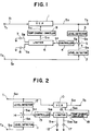
- Fig. 1 is an exemplary block diagram of a conventional closed-loop servo circuit.
- a process signal S1 fed to a process signal input terminal T1 is suppied to a VCA 2
- a control signal S2 fed to a control signal input terminal T2 is supplied to a first level detector 2.
- a VCA output signal S3 is delivered to an output terminal T3 and then is supplied to a second level detector 3.
- Output signals S4 and S5 of such first and second level detectors 2, 3 are added to each other by an adder 5 with the polarities thereof rendered mutually inverse.
- An output S6 of the adder 5 is delivered to a controller 4, which produces a control signal S7 for controlling the gain of the VCA 1 in accordance with the polarity of the input signal and then delivers the signal S7 to a limiter 6.
- a control signal S7 for increasing the gain of the VCA 1 is outputted from the controller 4 in case the adder output S6 is positive, whereby the gain of the VCA 1 is increased so that, in the two signals supplied to the adder 5, the negative signal S5 is gradually rendered greater, and the servo action is completed upon arrival of the adder output at zero.
- the limiter 6 is supplied with an upper limit setting signal S8 from an upper limit generator 7 and also with a lower limit setting signal S9 from a lower limit generator 8, and serves to change its output signal S10 between the upper and lower limit values.
- the output signal S10 from the limiter 6 is supplied to a temperature characteristic canceler 9 provided for canceling the temperature characteristic included in the control characteristics of the VCA 1.
- the signal S10 obtained from the limiter 6 is outputted as a gain control signal S11 from the temperature characteristic canceler 9 and then is delivered to the VCA 1.
- Fig. 1 representing an exemplary case where the servo circuit is formed into a closed loop
- Fig. 2 a similar operation is performed also in another case of Fig. 2 where the servo circuit is formed into an open loop.
- a constant voltage circuit (or constant current circuit) is required to cancel the temperature characteristic of the upper limit setting signal S8 and the lower limit setting signal S9.
- the provision of such cancel circuit renders the entire servo circuit configuration further complicated.
- the circuit configuration may be simplified by the use of a limiter 6 with a diode, zener diode or similar element, any limiter with such element has a temperature characteristic and therefore some disadvantages are induced inclusive of nonuniform operation and characteristic variations due to temperature fluctuations.
- a servo circuit for controlling the gain of a VCA by an output voltage of an integrator.
- both the level of an input signal to be processed and the level of a control signal are detected and calculated, and then the voltage held by the integrator is changed in accordance with the result of such calculation to change the output voltage, thereby controlling the gain of the VCA.
- Such gain control can be achieved by interrupting the current flowing in the integrator. More specifically, when the input current is interrupted, the integrator holds the voltage at such instant, so that the control voltage for the VCA is maintained at a fixed value to thereby retain the gain of the VCA at a certain fixed value.
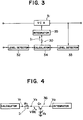
- Fig. 3 is a block diagram of an exemplary servo circuit based on the prior art.
- a VCA 31 a first level detector 32, a second level detector 33, a calculator 34, an integrator 35, and a switch 30.
- the switch 30 is provided for interrupting an input current flowing into the integrator 35. It has been generally customary in the conventional servo circuit to employ a MOS FET or a junction FET as the switch 30.
- the voltage V3 is rendered lower than the control voltage V4 by a value corresponding to the base-emitter voltage V BE .
- the base-emitter voltage V BE changes depending on the input current I i or the temperature, it follows that the voltage V3 also varies correspondingly thereto. Accordingly the input current I i changes in conformity with the temperature fluctuation and so forth, and the current inputted practically to the integrator 35 fails to be accurately proportional to the output voltage V1 of the calculator 34, hence inducing a disadvantage that the precision is deteriorated when the bipolar transistor Q1 is used as the switch 30.
- It is a first object of the present invention to provide a servo circuit comprising a variable gain amplifier (VCA), an amplitude limiter for setting an upper limit and a lower limit of a range in which the gain of the VCA is variable, and a gain control means so contrived that the temperature coefficient of the VCA and the temperature coefficients of the upper and lower limits of the gain variable range in the amplitude limiter are rendered mutually inverse in polarity, thereby canceling the temperature characteristic in the gain variable range to consequently eliminate the temperature characteristic in a simplified circuit configuration.
- VCA variable gain amplifier
- amplitude limiter for setting an upper limit and a lower limit of a range in which the gain of the VCA is variable
- a gain control means so contrived that the temperature coefficient of the VCA and the temperature coefficients of the upper and lower limits of the gain variable range in the amplitude limiter are rendered mutually inverse in polarity, thereby canceling the temperature characteristic in the gain variable range to consequently eliminate the temperature characteristic in a simplified
- a second object of the present invention is to provide a closed-loop servo circuit employing a limiter.
- a third object of the invention resides in providing an open-loop servo circuit employing a limiter.
- a fourth object of the invention is to provide a circuit for generating a voltage to determine the aforementioned gain control range.
- a fifth object of the invention is to provide a closed-loop servo circuit with a switch means.
- a sixth object of the invention resides in providing an open-loop servo circuit with a switch means.
- a seventh object of the invention is to provide a switch means and a specific circuit thereof adapted for use in both a closed-loop servo circuit and an open-loop servo circuit.
- An eighth object of the invention resides in providing another switch means and a specific circuit thereof adapted for use in both a closed-loop servo circuit and an open-loop servo circuit.
- a ninth object of the invention is to provide a servo circuit incorporated practically in a stereophonic audio apparatus.
- a servo circuit which comprises a variable gain amplifier where the gain is variable with a predetermined temperature coefficient to an absolute temperature, an amplitude limiter for setting an upper limit and a lower limit of the gain variable range of the amplifier, and a gain control range determiner for changing the upper and lower limits of the gain variable range in the amplitude limiter with a temperature coefficient inverse in polarity to that of the amplifier.
- a servo circuit which further comprises a signal processor for detecting and calculating the level of a control signal supplied to one input terminal and the level of a process signal supplied to the other terminal, and outputting a gain control signal in accordance with the level difference between the two input signals so as to control the gain of the variable gain amplifier.
- Fig. 5 is a block diagram of a closed-loop servo circuit according to a first embodiment of the present invention.
- the first embodiment is approximately similar to the aforementioned conventional servo circuit of Fig. 1 with regard to the circuit configuration as a whole. More specifically, a process signal S31 fed to a process signal input terminal T1 is supplied to a VCA 40, and a control signal S32 fed to a control signal input terminal T2 is supplied to a first level detector 42. In the meantime, the VCA output S33 is delivered to an output terminal T3 while being supplied to a second level detector 43. And respective output signals S34 and S35 of the first and second level detectors 42, 43 are added to each other by an adder 44 in such a manner that the polarities thereof are rendered mutually inverse. Thereafter an output S36 of the adder 44 is delivered to a controller 45.
- the controller 45 produces a control signal S37 for controlling the gain of the VCA 40 in accordance with the polarity of the input signal and then delivers the signal S37 to a limiter 46.
- a control signal S37 for increasing the gain of the VCA 40 is outputted from the controller 45 in case the adder output S36 is positive, whereby the gain of the VCA 40 is increased so that, in the two signals supplied to the adder 44, the negative signal is gradually rendered greater, and the servo action is completed upon arrival of the adder output S36 at zero.
- the limiter 46 is supplied with an upper limit setting signal S38 from an upper limit generator 48 in a gain control range determiner 47 and also with a lower limit setting, signal S39 from a lower limit generator 48, and serves to change its output signal S40, which corresponds to the gain control signal S11 in Fig. 1, between such upper and lower limit values.
- the output signal S40 from the limiter 46 is supplied as a gain control signal to the VCA 40, which then performs an operation of varying the gain within the range determined by the gain control range determiner 47.
- the gain control in the VCA 40 is generally executed by, as shown in Fig. 6, changing the ratio of the output currents, which flow in transistors Q2 and Q3 of a differential amplifier 51 respectively, by means of a control voltage adjuster 52 to thereby change the operating state of the circuit.
- the ratio of the output currents I1 and T2 of the transistors Q2 and Q3 is expressed as follows in relation to the control voltage Vc of the control voltage adjuster 52.
- I1/I2 exp (q Vc / kT)
- Meanswhile the means for generating a voltage directly proportional to the absolute temperature T may be such as shown in a circuit diagram of Fig. 7 which is considered adequate to realize an IC configuration.
- Fig. 7 represents an exemplary current mirror circuit comprising first through fourth constant current sources 55a, 55b, 55c, 55d; first and second transistors Q4, Q5; a resistor R2 connected between the emitter of the transistor Q5 and the ground; and a resistor R3 connected between the constant current source 55d and the ground. The output voltage of such current mirror circuit is obtained across the resistor R3.
- the output current I out flowing in the resistor R3 is expressed as follows in relation to the ratio 1 : n between the emitter area of the transistor Q4 and that of the transistor Q5.
- I OUT ⁇ (2kT/q) ⁇ l n ⁇ n ⁇ / R2
- V LIMIT (R3 / R2) ⁇ (2kT / q) ⁇ l n ⁇ n
- the output voltage V LIMIT is in direct proportion to the absolute temperature T. Consequently, under the conditions that the circuit of Fig. 7 is used for both the upper limit generator 48 and the lower limit generator 49 in Fig. 5, if the voltages V LIMIT outputted from such limit generators are utilized as upper and lower limit values of the control voltage for the VCA 40, then the temperature characteristics in the gain control range of the entire servo circuit cancel each other to become zero.
- an improved servo circuit free from a temperature characteristic in the gain control range can be accomplished by the present invention with a simplified circuit configuration.
- the output signal of the VCA 40 is inputted directly to the level detector 43.
- the circuit configuration may be so modified as to execute some signal process before supplying the VCA output signal to the level detector 43.
- the characteristics of the controller 45 and the level detectors 42, 43 can be set freely to desired ones.
- the servo circuit of the present invention is properly applicable also to an open-loop type as shown in a circuit block diagram of Fig. 8.
- each of the upper limit setting signal S48 and the lower limit setting signal S49 is supplied in the form of a voltage to the limiter 66, such signals S48 and S49 may be provided in the form of a current as well. In the latter case where the current signals are supplied, the output current I OUT in Fig. 7 may be directly taken out and fed to the limiter 66.
- the servo circuit according to the above embodiment is formed into an IC configuration, the existing means for generating a voltage (current) directly proportional to the temperature as shown in Fig. 7 is utilizable since it is generally incorporated in an IC, and therefore the servo circuit can be constituted free from a temperature characteristic without causing any substantial enlargement of the circuit scale.
- the present invention is so contrived that the temperature coefficient of the VCA and that of the amplitude limiter for setting upper and lower limits of the gain variable range in the VCA are rendered mutually inverse in polarity, so that if the characteristic of the VCA and the temperature characteristic within the gain variable range preset by the amplitude limiter are changed due to temperature fluctuations, such changes cancel each other to consequently reduce to zero the temperature characteristic in the gain control range of the entire servo circuit.
- the present invention is so contrived that the temperature coefficient of the VCA and that of the amplitude limiter for setting upper and lower limits of the gain variable range in the VCA are rendered mutually inverse in polarity, so that if the characteristic of the VCA and the temperature characteristic within the gain variable range preset by the amplitude limiter are changed due to temperature fluctuations, such changes cancel each other to consequently reduce to zero the temperature characteristic in the gain control range of the entire servo circuit.
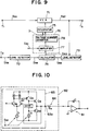
- Fig. 9 is a block diagram of a servo circuit according to a third embodiment of-the present invention.
- the third embodiment is equipped with a switch circuit 76 which consists of a voltage output type amplifier 77 and a voltage-current converter 78 and is interposed between a calculator 74 and an integrator 75.
- a process signal S55 fed to a process signal input terminal T1 is supplied to a VCA 71, and a control signal S56 fed to a control signal input terminal T2 is supplied to a first level detector 72.
- a VCA output signal S57 is delivered to an output terminal T3 while being supplied also to a second level detector 73.
- Such output signals S58 and S59 of the first and second level detectors 72, 73 are fed to a calculator 74.
- the calculator 74 compares the received signals S58 and S59 with each other and, in accordance with the result of such comparison, produces a signal S60 for controlling the gain of the VCA 71. For example, when the output signal S59 of the second level detector 73 is smaller than the output signal S58 of the first level detector 72, there is outputted a gain control signal S60 to increase the gain of the VCA 71.
- the gain control signal S60 outputted from the calculator 74 is supplied to a voltage output type amplifier 77 constituting the switch circuit 76.
- the amplifier 77 is provided to serve as a buffer amplifier and is turned on or off in conformity with an output state control signal S61 fed to the control input terminal.
- the circuit diagram of Fig. 10 represents an example of the amplifier 77.
- an amplifier 83 is a type generally used and, when constant current sources are controlled in a normal operating state by the output state control signal S61, currents I1 and I2 of predetermined values are caused to flow so that the amplifier 83 itself functions as an ordinary buffer amplifier.
- the signal voltage applied to the amplifier 83 is outputted without being amplified at all, whereby the output voltage of the calculator 74 is fed without any change to an output terminal 83a of the amplifier 83.
- an integrator 81 is supplied with a current of the value obtained through division of the potential difference between the output terminal 83a of the amplifier 83 and the ground by the resistance of a resistor R4, and the voltage held by the integrator 81 is changed in accordance with such current value to thereby perform the servo action. Since the bipolar transistor is not employed solely to serve as an analog switch, there occurs none of an error which may otherwise be derived from incomplete insulation between the switching transistor driver and the integrator.
- the transistor in the output stage is not supplied with a bias current and is therefore turned off, whereby the output terminal 83a of the amplifier 83 comes to have a high impedance.
- the impedance at one end of the resistor R4 is also rendered high so that the input current I i to the integrator 81 is reduced to zero.
- the voltage at the instant of reduction of the currents I1 and I2 of the amplifier 83 to zero is held by the integrator 81, hence maintaining the gain of the VCA 71 to the value at such instant.
- the embodiment mentioned above represents the configuration of an exemplary closed-loop servo circuit where the gain of the VCA 71 is determined by the result of a comparison between the VCA output signal S57 and the control signal S56.
- the configuration may be modified to an open-loop servo circuit of Fig. 11 where a direct comparison is executed between a process signal S71 and a control signal S72.
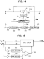
- the servo circuit of the above configuration is adapted for use in, for example, a matrix surround circuit of a sound multiplexer as shown in a block diagram of Fig. 15.
- an opposite-phase component (L - R) of a right channel signal R and a left channel signal L fed to one input terminal is supplied to a process signal input terminal T1 of the servo circuit while being supplied also to a first level detector 131 via a first buffer amplifier 130.
- an in-phase component (L + R) fed to the other input terminal is supplied to a control signal input terminal T2 of the servo circuit while being supplied also to a second level detector 133 via a second buffer amplifier 132.
- respective detection outputs Sx and Sy of the first and second level detectors 131, 133 are supplied to a comparator 134 which detects the ratio of the opposite-phase component (L - R) and the in-phase component (L + R). In case the ratio thus detected is greater than a predetermined value, an output state control signal S97 for operating an amplifier 97 of the servo circuit in a normal state is outputted from the comparator 134 to the servo circuit. Consequently the servo circuit is placed in a normal operating state wherein an output signal (L - R)′ obtained through controlling the level of the opposite-phase component (L - R) by the gain conforming with the in-phase component (L + R) is delivered to an output terminal T3.
- the comparator 134 provides an output state control signal S97 to halt the operation of the amplifier 97 in the servo circuit. Then the impedance at the output terminal 97a of the amplifier 97 is rendered high to consequently block a current inflow to the integrator 95 as described. Therefore the voltage held by the integrator 95 is maintained to the value at such instant, hence preventing deterioration of the signal-to-noise ratio which may otherwise be caused by an excessive increase of the gain of the VCA 91 derived from an excessive level reduction of the opposite-phase component (L - R).
- a voltage output type amplifier selectively switchable to either a normal operating state for directly delivering an input gain control signal to an output terminal or a signal interrupting state for retaining the output terminal at a high impedance is disposed. between a signal processing circuit, which outputs the gain control signal in accordance with the level difference between a process signal fed to one input terminal and a control signal fed to the other input terminal, and a voltage holding circuit for generating a control voltage in conformity with the gain control signal and controlling the gain of the VCA; and a current proportional to the output voltage of the amplifier is generated and supplied to the voltage holding circuit.
- Fig. 12 is a block diagram of a servo circuit according to a fifth embodiment of the present invention.
- a switch circuit 106 disposed between a calculator 104 and an integrator 105 is composed of a current output type amplifier 107.
- a process signal S81 fed to a process signal input terminal T1 is supplied to a VCA 101, and a control signal S82 fed to a control signal input terminal T2 is supplied to a first level detector 102.
- a VCA output signal S83 is delivered as a servo output signal to an output terminal T3 while being supplied also to a second level detector 103.
- respective output signals S84 and S85 of the first and second level detectors 102, 103 are supplied to a calculator 104. Then the calculator 104 compares the received signals S84 and S85 with each other and produces, in accordance with the result of such comparison, a signal S86 for controlling the gain of the VCA 101.
- the output signal S85 of the second level detector 103 is smaller than the output signal S84 of the first level detector 102, there is produced a gain control signal S86 for increasing the gain of the VCA 101 so that a servo action is performed to increase the level of the output signal S85 from the second level detector 103.
- the gain control signal S86 outputted from the calculator 104 is supplied to an amplifier 107 constituting a switch circuit 106.
- the amplifier 107 is provided to serve as a buffer amplifier and, in this embodiment, consists of a current output type amplifier 110 as shown in a circuit diagram of Fig. 13.
- the amplifier 110 comprises a current generator 111, a controller 112 and an output selector 113.
- the current generator 111 is composed of a pair of transistors Q11, Q12 and three constant current sources a , b , c to function as a differential amplifier.
- a current I flowing in the constant current source c interposed between the mutually connected emitters and the ground is maintained constant, while currents I1, I2 flowing in the constant current sources a , b respectively are changed in accordance with the gain control signal S86 outputted from the calculator 104 and supplied to the control electrodes of the transistors Q11, Q12, whereby the currents I1, I2 are rendered proportionate to the gain control signal S86.
- the output selector 113 is composed of four transistors Q13 - Q16 and three constant current sources d , e , f wherein signals for turning on or off the transistors Q13 - Q16 are supplied to the control electrodes of the individual transistors. As indicated by broken-line arrows, a mirror current from the constant current source a flows into the constant current source d , and a mirror current from the constant current source d flows into the constant current source e . Further a mirror current from the constant current source b flows into the constant current source f . Thus, each of the currents flowing into the constant current sources d , e , f in the output selector 113 is rendered proportional to the gain control signal S86.
- the output selector 113 is driven under the conditions that the potentials at the output terminals 112a, 112b, 112c, 112d of the controller 112 are turned respectively to "H” (high), “L” (low), “H", “L” levels in conformity with the output state control signal S87 fed to the control input terminal of the controller 112, whereby a current I i proportional to the gain control signal S86 is caused to flow in the output terminal 107a.
- the current caused to flow in the output terminal 107a is reduced to zero. Accordingly, when the controller 112 is controlled in a normal operating state by the output state control signal S87, the input current I i of a predetermined value conforming with the gain control output signal S86 is provided from the current output type amplifier 107 and then is supplied to an integrator 105. Thus, a servo action is performed as the voltage held by the integrator 105 is changed in accordance with the input current I i . In this case, since the bipolar transistor is not employed solely to serve as an analog switch, there occurs none of an error which may otherwise be derived from incomplete insulation between the switching transistor driver and the integrator.
- the input current I i to the integrator 105 is reduced to zero, and the voltage obtained upon reduction of the output current of the amplifier 107 to zero is held by the integrator 105, so that the gain of the VCA 101 is maintained to the value at such instant.
- the fifth embodiment mentioned above represents an exemplary configuration of a closed-loop servo circuit where the gain of the VCA 101 is determined by the result of a comparison between the VCA output signal S83 and the control signal S82.
- the configuration may be modified to an open-loop servo circuit where, as shown in a block diagram of Fig. 14, a process signal S91 is compared with a control signal S92.
- the servo circuit of the above configuration according to a sixth embodiment of the invention is adapted for use in a matrix surround circuit of a sound multiplexer as shown in a block diagram of Fig. 15.
- a current output type amplifier selectively switchable to either a first operating state for delivering a current from an output terminal in conformity to a gain control signal obtained from a signal processing circuit or a second operating state for reducing to zero the current delivered from the output terminal is disposed between the signal processing circuit, which outputs therefrom the gain control signal in accordance with the level difference between a process signal fed to one input terminal and a control signal fed to the other input terminal, and a voltage holding circuit for controlling the gain of the VCA in accordance with the gain control signal, wherein the output current of the amplifier is supplied to the voltage holding circuit. Therefore, a desired operation performed by an FET switch circuit can be achieved similarly by the use of a bipolar-transistor switch circuit as well. Consequently, when such servo circuit is formed into an IC configuration, it becomes possible to attain high-precision operating characteristic merely by a bipolar transistor manufacturing process, hence minimizing the number of required process steps to eventually curtail the production cost.
Landscapes
- Engineering & Computer Science (AREA)
- Power Engineering (AREA)
- Multimedia (AREA)
- Optical Recording Or Reproduction (AREA)
- Control Of Amplification And Gain Control (AREA)
- Feedback Control In General (AREA)
- Tone Control, Compression And Expansion, Limiting Amplitude (AREA)
- Amplifiers (AREA)
Priority Applications (1)
| Application Number | Priority Date | Filing Date | Title |
|---|---|---|---|
| EP94113117A EP0638997B1 (fr) | 1990-08-24 | 1991-08-22 | Circuit de commande |
Applications Claiming Priority (6)
| Application Number | Priority Date | Filing Date | Title |
|---|---|---|---|
| JP2223560A JP3018435B2 (ja) | 1990-08-24 | 1990-08-24 | サーボ回路 |
| JP223560/90 | 1990-08-24 | ||
| JP2236389A JP2979607B2 (ja) | 1990-09-06 | 1990-09-06 | サーボ回路 |
| JP236389/90 | 1990-09-06 | ||
| JP2236390A JP2979608B2 (ja) | 1990-09-06 | 1990-09-06 | サーボ回路 |
| JP236390/90 | 1990-09-06 |
Related Child Applications (2)
| Application Number | Title | Priority Date | Filing Date |
|---|---|---|---|
| EP94113117A Division EP0638997B1 (fr) | 1990-08-24 | 1991-08-22 | Circuit de commande |
| EP94113117.9 Division-Into | 1991-08-22 |
Publications (2)
| Publication Number | Publication Date |
|---|---|
| EP0473370A1 true EP0473370A1 (fr) | 1992-03-04 |
| EP0473370B1 EP0473370B1 (fr) | 1996-05-15 |
Family
ID=27330798
Family Applications (2)
| Application Number | Title | Priority Date | Filing Date |
|---|---|---|---|
| EP91307759A Expired - Lifetime EP0473370B1 (fr) | 1990-08-24 | 1991-08-22 | Circuit de contrÔle de gain |
| EP94113117A Expired - Lifetime EP0638997B1 (fr) | 1990-08-24 | 1991-08-22 | Circuit de commande |
Family Applications After (1)
| Application Number | Title | Priority Date | Filing Date |
|---|---|---|---|
| EP94113117A Expired - Lifetime EP0638997B1 (fr) | 1990-08-24 | 1991-08-22 | Circuit de commande |
Country Status (5)
| Country | Link |
|---|---|
| US (1) | US5166559A (fr) |
| EP (2) | EP0473370B1 (fr) |
| KR (1) | KR100191109B1 (fr) |
| DE (2) | DE69119514T2 (fr) |
| TW (1) | TW258797B (fr) |
Cited By (2)
| Publication number | Priority date | Publication date | Assignee | Title |
|---|---|---|---|---|
| EP0645770A3 (fr) * | 1993-09-24 | 1999-02-17 | Fujitsu Limited | Circuit de réglage du niveau zéro du convertisseur AN dans une unité à disques magnétiques |
| CN110366819A (zh) * | 2017-02-28 | 2019-10-22 | 思睿逻辑国际半导体有限公司 | 具有受控功率供应的用于放大音频信号的放大器电路 |
Families Citing this family (6)
| Publication number | Priority date | Publication date | Assignee | Title |
|---|---|---|---|---|
| JPH08274559A (ja) * | 1995-04-03 | 1996-10-18 | Oki Electric Ind Co Ltd | 出力電力制御装置 |
| US6636722B1 (en) | 2000-09-12 | 2003-10-21 | Tektronix, Inc. | Broadband receiver amplitude/phase normalization using a broadband temperature compensated noise source and a pseudo random sequence generator |
| US6556022B2 (en) * | 2001-06-29 | 2003-04-29 | Intel Corporation | Method and apparatus for local parameter variation compensation |
| US7259620B2 (en) * | 2005-06-27 | 2007-08-21 | Linear Technology Corporation | Wide dynamic range switching variable gain amplifier and control |
| US7656227B1 (en) | 2008-02-26 | 2010-02-02 | Pmc-Sierra, Inc. | Techniques to control amplifier gain over process, voltage, and/or temperature (PVT) variations |
| CN101938255B (zh) * | 2010-09-16 | 2012-09-05 | 中国电子科技集团公司第二十四研究所 | 低于100mW低功耗真对数放大器 |
Citations (1)
| Publication number | Priority date | Publication date | Assignee | Title |
|---|---|---|---|---|
| US4101841A (en) * | 1976-09-03 | 1978-07-18 | Hitachi, Ltd. | Gain control circuit |
Family Cites Families (8)
| Publication number | Priority date | Publication date | Assignee | Title |
|---|---|---|---|---|
| US3770984A (en) * | 1971-03-03 | 1973-11-06 | Harris Intertype Corp | Fast recovery low distortion limiter circuit |
| US3879674A (en) * | 1973-12-27 | 1975-04-22 | Burroughs Corp | Automatic gain control circuit |
| US4238738A (en) * | 1977-06-15 | 1980-12-09 | Tokyo Shibaura Electric Co., Ltd. | Temperature-compensated amplifier circuit |
| JPS5422512U (fr) * | 1977-07-15 | 1979-02-14 | ||
| GB1568513A (en) * | 1977-10-07 | 1980-05-29 | Secr Defence | Automatic signal level control system |
| US4297645A (en) * | 1979-09-20 | 1981-10-27 | Nippon Electric Co., Ltd. | Automatic gain control circuit comprising a circuit for comparing a modulated signal with an envelope detected signal |
| FR2520952A1 (fr) * | 1982-02-03 | 1983-08-05 | Trt Telecom Radio Electr | Dispositif de controle automatique de gain (cag) a action rapide |
| US5030924A (en) * | 1989-03-30 | 1991-07-09 | Silicon Systems, Inc. | Temperature compensated exponential gain control circuit |
-
1991
- 1991-08-15 TW TW080106479A patent/TW258797B/zh active
- 1991-08-21 KR KR1019910014378A patent/KR100191109B1/ko not_active Expired - Fee Related
- 1991-08-21 US US07/748,047 patent/US5166559A/en not_active Expired - Lifetime
- 1991-08-22 DE DE69119514T patent/DE69119514T2/de not_active Expired - Fee Related
- 1991-08-22 EP EP91307759A patent/EP0473370B1/fr not_active Expired - Lifetime
- 1991-08-22 DE DE69128652T patent/DE69128652T2/de not_active Expired - Fee Related
- 1991-08-22 EP EP94113117A patent/EP0638997B1/fr not_active Expired - Lifetime
Patent Citations (1)
| Publication number | Priority date | Publication date | Assignee | Title |
|---|---|---|---|---|
| US4101841A (en) * | 1976-09-03 | 1978-07-18 | Hitachi, Ltd. | Gain control circuit |
Non-Patent Citations (3)
| Title |
|---|
| PATENT ABSTRACTS OF JAPAN vol. 12, no. 3 (E-570)7 January 1988 & JP-A-62 165 415 ( MATSUSHITA ELECTRIC IND CO LTD ) 22 July 1987 * |
| PATENT ABSTRACTS OF JAPAN vol. 6, no. 123 (E-117)8 July 1982 & JP-A-57 052 239 ( SONY CORP ) 27 March 1982 * |
| PATENT ABSTRACTS OF JAPAN vol. 8, no. 221 (E-271)9 October 1984 & JP-A-59 104 826 ( SONY K.K. ) 16 June 1984 * |
Cited By (3)
| Publication number | Priority date | Publication date | Assignee | Title |
|---|---|---|---|---|
| EP0645770A3 (fr) * | 1993-09-24 | 1999-02-17 | Fujitsu Limited | Circuit de réglage du niveau zéro du convertisseur AN dans une unité à disques magnétiques |
| CN110366819A (zh) * | 2017-02-28 | 2019-10-22 | 思睿逻辑国际半导体有限公司 | 具有受控功率供应的用于放大音频信号的放大器电路 |
| CN110366819B (zh) * | 2017-02-28 | 2023-01-24 | 思睿逻辑国际半导体有限公司 | 具有受控功率供应的用于放大音频信号的放大器电路 |
Also Published As
| Publication number | Publication date |
|---|---|
| US5166559A (en) | 1992-11-24 |
| KR100191109B1 (ko) | 1999-06-15 |
| DE69119514T2 (de) | 1996-09-26 |
| EP0473370B1 (fr) | 1996-05-15 |
| DE69128652T2 (de) | 1998-05-14 |
| EP0638997A1 (fr) | 1995-02-15 |
| EP0638997B1 (fr) | 1998-01-07 |
| DE69119514D1 (de) | 1996-06-20 |
| KR920005466A (ko) | 1992-03-28 |
| TW258797B (fr) | 1995-10-01 |
| DE69128652D1 (de) | 1998-02-12 |
Similar Documents
| Publication | Publication Date | Title |
|---|---|---|
| KR20010082344A (ko) | 레벨 시프트 회로 | |
| JPH04324192A (ja) | 高速差動増幅器 | |
| US5166559A (en) | Servo circuit having variable gain amplifier and temperature compensation characteristics | |
| US4451800A (en) | Input bias adjustment circuit for amplifier | |
| US3828266A (en) | Signal control circuit | |
| US5742204A (en) | Digitally programmable differential attenuator with tracking common mode reference | |
| US4928074A (en) | Automatic gain control circuit | |
| CA1301863C (fr) | Circuit amplificateur commande par le gain | |
| NZ203750A (en) | Cascade amplifier:gain of stages varied in opposition | |
| EP0420128B1 (fr) | Circuit détecteur pour signaux modulés en amplitude | |
| KR860000440B1 (ko) | 신호레벨제어회로 | |
| US4360786A (en) | Variable-gain differential amplifier | |
| JPH0312721B2 (fr) | ||
| JP2740211B2 (ja) | 映像信号補正回路 | |
| US5119041A (en) | High gain differential current amplifier having a low output voltage | |
| JP2558253B2 (ja) | 温度補償型カレントスイツチ回路 | |
| JPH0444407A (ja) | 利得制御回路 | |
| JP3305864B2 (ja) | 信号変換回路 | |
| US4629998A (en) | Variable gain equalizer with a mirror circuit having opposite phase relationship between input and output currents | |
| JPS62117404A (ja) | 可変利得増幅回路 | |
| JPS60212068A (ja) | フイ−ドバツククランプ回路 | |
| JPS5837722B2 (ja) | 可変利得増幅器 | |
| JP2722769B2 (ja) | 利得制御回路 | |
| JP3018435B2 (ja) | サーボ回路 | |
| KR960008145Y1 (ko) | 전류원 회로 |
Legal Events
| Date | Code | Title | Description |
|---|---|---|---|
| PUAI | Public reference made under article 153(3) epc to a published international application that has entered the european phase |
Free format text: ORIGINAL CODE: 0009012 |
|
| AK | Designated contracting states |
Kind code of ref document: A1 Designated state(s): DE FR GB |
|
| 17P | Request for examination filed |
Effective date: 19920520 |
|
| 17Q | First examination report despatched |
Effective date: 19940426 |
|
| GRAH | Despatch of communication of intention to grant a patent |
Free format text: ORIGINAL CODE: EPIDOS IGRA |
|
| GRAA | (expected) grant |
Free format text: ORIGINAL CODE: 0009210 |
|
| AK | Designated contracting states |
Kind code of ref document: B1 Designated state(s): DE FR GB |
|
| XX | Miscellaneous (additional remarks) |
Free format text: TEILANMELDUNG 94113117.9 EINGEREICHT AM 22/08/91. |
|
| REF | Corresponds to: |
Ref document number: 69119514 Country of ref document: DE Date of ref document: 19960620 |
|
| ET | Fr: translation filed | ||
| PLBE | No opposition filed within time limit |
Free format text: ORIGINAL CODE: 0009261 |
|
| STAA | Information on the status of an ep patent application or granted ep patent |
Free format text: STATUS: NO OPPOSITION FILED WITHIN TIME LIMIT |
|
| 26N | No opposition filed | ||
| REG | Reference to a national code |
Ref country code: GB Ref legal event code: IF02 |
|
| PGFP | Annual fee paid to national office [announced via postgrant information from national office to epo] |
Ref country code: FR Payment date: 20050809 Year of fee payment: 15 |
|
| PGFP | Annual fee paid to national office [announced via postgrant information from national office to epo] |
Ref country code: GB Payment date: 20050817 Year of fee payment: 15 |
|
| PGFP | Annual fee paid to national office [announced via postgrant information from national office to epo] |
Ref country code: DE Payment date: 20050818 Year of fee payment: 15 |
|
| PG25 | Lapsed in a contracting state [announced via postgrant information from national office to epo] |
Ref country code: DE Free format text: LAPSE BECAUSE OF NON-PAYMENT OF DUE FEES Effective date: 20070301 |
|
| GBPC | Gb: european patent ceased through non-payment of renewal fee |
Effective date: 20060822 |
|
| REG | Reference to a national code |
Ref country code: FR Ref legal event code: ST Effective date: 20070430 |
|
| PG25 | Lapsed in a contracting state [announced via postgrant information from national office to epo] |
Ref country code: GB Free format text: LAPSE BECAUSE OF NON-PAYMENT OF DUE FEES Effective date: 20060822 |
|
| PG25 | Lapsed in a contracting state [announced via postgrant information from national office to epo] |
Ref country code: FR Free format text: LAPSE BECAUSE OF NON-PAYMENT OF DUE FEES Effective date: 20060831 |