EP0475259A2 - Verfahren zur Herstellung eines Halbleiterbauelementes - Google Patents
Verfahren zur Herstellung eines Halbleiterbauelementes Download PDFInfo
- Publication number
- EP0475259A2 EP0475259A2 EP91114907A EP91114907A EP0475259A2 EP 0475259 A2 EP0475259 A2 EP 0475259A2 EP 91114907 A EP91114907 A EP 91114907A EP 91114907 A EP91114907 A EP 91114907A EP 0475259 A2 EP0475259 A2 EP 0475259A2
- Authority
- EP
- European Patent Office
- Prior art keywords
- grinding
- substrate
- micro
- gaas substrate
- semiconductor element
- Prior art date
- Legal status (The legal status is an assumption and is not a legal conclusion. Google has not performed a legal analysis and makes no representation as to the accuracy of the status listed.)
- Granted
Links
Images


Classifications
-
- H—ELECTRICITY
- H10—SEMICONDUCTOR DEVICES; ELECTRIC SOLID-STATE DEVICES NOT OTHERWISE PROVIDED FOR
- H10P—GENERIC PROCESSES OR APPARATUS FOR THE MANUFACTURE OR TREATMENT OF DEVICES COVERED BY CLASS H10
- H10P50/00—Etching of wafers, substrates or parts of devices
- H10P50/60—Wet etching
- H10P50/64—Wet etching of semiconductor materials
- H10P50/642—Chemical etching
- H10P50/646—Chemical etching of Group III-V materials
-
- H—ELECTRICITY
- H10—SEMICONDUCTOR DEVICES; ELECTRIC SOLID-STATE DEVICES NOT OTHERWISE PROVIDED FOR
- H10P—GENERIC PROCESSES OR APPARATUS FOR THE MANUFACTURE OR TREATMENT OF DEVICES COVERED BY CLASS H10
- H10P52/00—Grinding, lapping or polishing of wafers, substrates or parts of devices
-
- H—ELECTRICITY
- H10—SEMICONDUCTOR DEVICES; ELECTRIC SOLID-STATE DEVICES NOT OTHERWISE PROVIDED FOR
- H10P—GENERIC PROCESSES OR APPARATUS FOR THE MANUFACTURE OR TREATMENT OF DEVICES COVERED BY CLASS H10
- H10P54/00—Cutting or separating of wafers, substrates or parts of devices
-
- Y—GENERAL TAGGING OF NEW TECHNOLOGICAL DEVELOPMENTS; GENERAL TAGGING OF CROSS-SECTIONAL TECHNOLOGIES SPANNING OVER SEVERAL SECTIONS OF THE IPC; TECHNICAL SUBJECTS COVERED BY FORMER USPC CROSS-REFERENCE ART COLLECTIONS [XRACs] AND DIGESTS
- Y10—TECHNICAL SUBJECTS COVERED BY FORMER USPC
- Y10S—TECHNICAL SUBJECTS COVERED BY FORMER USPC CROSS-REFERENCE ART COLLECTIONS [XRACs] AND DIGESTS
- Y10S148/00—Metal treatment
- Y10S148/051—Etching
-
- Y—GENERAL TAGGING OF NEW TECHNOLOGICAL DEVELOPMENTS; GENERAL TAGGING OF CROSS-SECTIONAL TECHNOLOGIES SPANNING OVER SEVERAL SECTIONS OF THE IPC; TECHNICAL SUBJECTS COVERED BY FORMER USPC CROSS-REFERENCE ART COLLECTIONS [XRACs] AND DIGESTS
- Y10—TECHNICAL SUBJECTS COVERED BY FORMER USPC
- Y10S—TECHNICAL SUBJECTS COVERED BY FORMER USPC CROSS-REFERENCE ART COLLECTIONS [XRACs] AND DIGESTS
- Y10S148/00—Metal treatment
- Y10S148/135—Removal of substrate
Definitions
- the present invention relates to a method of manufacturing a semiconductor device and more particularly relates to a treatment of a back surface of a GaAs substrate on which a semiconductor device is formed.
- a semiconductor element formed on a GaAs Substrate a chemical compound semiconductor, has a difficulty to dissipate heat generated from the device formed on a surface of the GaAs substrate, since thermal conductivity of GaAs is 1/3 times as low as that of Si. It adversely affects characteristics of the device. And, it is necessary to thin the substrate and assure a good dissipation of heat.
- GaAs is brittle compared with Si and easy to be cracked and/or broken off. So, chip cracking is easily caused starting from fine flaws and the like yielded at a thinning process.
- a grinding stone with fine grains must be used to perform the aforementioned mirror grinding. It means only a small amount to be ground off per a unit time and taking a long time of period to grind off a predetermined amount. It results in low productivity for mass production and in making a process complicated because of a need of facilities for mirror grinding.
- the present invention provides a method of manufacturing a semiconductor device comprising the steps of: forming a semiconductor element on one of major surfaces of a GaAs substrate; a grinding the substrate to make the GaAs substrate to a predetermined thickness by grinding the other surface of the GaAs substrate with a grinding stone having an average grain size of 6 micro-meters or larger; and an chemical etching the other surface of the substrate by 0.6 micro-meters or more just after the grinding step, without any further grinding treatment done on the other surface, just after the grinding step.
- a grinding stone with a grain size of 6 micro-meters or larger is used to grind a GaAs substrate, on which a semiconductor element is formed, in a short time of period. And thereafter a chemical etching removes a deformed layer on a back surface of the substrate caused by the above mentioned grinding step. It enables to manufacture a GaAs substrate with high strength, in a short time of period.
- the characterizing process is comprised of step 1 of forming a semiconductor element on a surface of the GaAs substrate, step 2 of grinding off a back side of the GaAs substrate on which the semiconductor element is formed, and a step 3 of performing chemical etching to remove the back side by a predetermined thickness, just after the grinding step.
- a semiconductor element is formed on one of main surfaces of the GaAs wafer first.
- the semiconductor element is, for example Shottky-gate type field effect transistor or the like and on the one main surface, monolithic microwave integrated circuit or the like is formed by such field effect transistors.
- This step is performed utilizing photo-lithograph technique, ion implantation technique and the like. These are not described in detail here, as conventionally well known.
- the one surface of the GaAs wafer on which the semiconductor element is formed is completely covered with a film made of organic material etc. and thereafter the wafer is mounted on a grinding machine by holding the covered surface thereof on a rotational stage of the grinding machine to grind the back side surface of the wafer.
- the rotational stage mounting the wafer thereon is rotated and forwarded to a grinding stone rotating and located so as to face to the rotational stage and as the result the back side of the wafer is made in contact with the grinding stone to be ground.
- a wafer rotation down-feed method is used, as grinding resistance can be kept constant in it.
- a diamond grinding stone with an average grain size of 6 micro-meters or larger is used.
- Fig.2 shows a relation between an average grain of a diamond grinding stone (horizontal axis) and a roughness (R max) (vertical axis) in the surface to be finished. As shown in Fig.
- the back surface of the wafer is chemically etched without any further grinding treatment.
- the side of the GaAs substrate on which the semiconductor element is formed is covered with a protection film, before the substrate is soaked in a mixture of ammonia, hydrogen dioxide and water.
- the mixture should have a very low etching speed.
- Various liquid mixture can be used as an etchant, for example, phosphoric based etchant, potassium-hydroxide based etchant or aqua regia etc.
- the step chemically etches the back surface of the GaAs wafer by 0.6 micro-meters or more.
- etching should be 0.6 micron-meters or more because the thickness of the deformed layer yielded on the back surface of the GaAs wafer by the previous grinding is about 0.6 micro-meters.
- a bend or the like in the wafer can be satisfactorily removed only by removing the deformed layer.
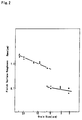
- Fig. 3 shows a relation between etching amount and surface condition factor(K) on the back surface of the substrate, and the surface condition factor corresponds to a bend degree of the wafer.
- the relation shown in Fig. 3 proves the etching amount is sufficient, because K value is restored to the same level as that of polished surface at 0.6 micro-meters etching (See "Technique of GaAs wafer mirror grinding" in Super-Precision Machining manual).
- a broken line shows polished surface, white dots non-mirror grinding (rough grinding) and filled dots mirror grinding respectively.
- the applicant measured "the Fracture Stress" of GaAs substrates respectively manufactured by the following two methods 1 and 2, by two different methods, one is a so-called “Four-Point Loading method” and the other is a so-called “Biaxial Loading method",
- Table I shows "Fracture Stress data” obtained by the Four-point Loading method and Table II shows “Fracture Stress data” obtained by the Biaxial Loading method.
- GaAs wafer is divided into individual IC chip by a dicing machine.
- the divided IC chip is die bonded on a ceramic plate by an eutectic alloy using AuSu etc.
- the back surface of the GaAs is metalized by Ti evaporation etc. and further Au layer is deposited thereon.
- a combination of the high speed grinding and the chemical etching enables a semiconductor element with sufficiently strong GaAs substrate to be manufactured in a short time of period.
- mirror grinding treatment can be eliminated, which simplifies manufacturing facilities and shortens manufacturing time. Consequently the present invention enables the semiconductor element to be manufactured at a low cost.
Landscapes
- Mechanical Treatment Of Semiconductor (AREA)
- Weting (AREA)
Applications Claiming Priority (2)
| Application Number | Priority Date | Filing Date | Title |
|---|---|---|---|
| JP235152/90 | 1990-09-05 | ||
| JP2235152A JP2610703B2 (ja) | 1990-09-05 | 1990-09-05 | 半導体素子の製造方法 |
Publications (3)
| Publication Number | Publication Date |
|---|---|
| EP0475259A2 true EP0475259A2 (de) | 1992-03-18 |
| EP0475259A3 EP0475259A3 (en) | 1992-12-16 |
| EP0475259B1 EP0475259B1 (de) | 1995-08-30 |
Family
ID=16981823
Family Applications (1)
| Application Number | Title | Priority Date | Filing Date |
|---|---|---|---|
| EP91114907A Expired - Lifetime EP0475259B1 (de) | 1990-09-05 | 1991-09-04 | Verfahren zur Herstellung eines Halbleiterbauelementes |
Country Status (8)
| Country | Link |
|---|---|
| US (1) | US5122481A (de) |
| EP (1) | EP0475259B1 (de) |
| JP (1) | JP2610703B2 (de) |
| KR (1) | KR940002915B1 (de) |
| AU (1) | AU649063B2 (de) |
| CA (1) | CA2050675A1 (de) |
| DE (1) | DE69112545T2 (de) |
| DK (1) | DK0475259T3 (de) |
Cited By (6)
| Publication number | Priority date | Publication date | Assignee | Title |
|---|---|---|---|---|
| EP0603514A3 (de) * | 1992-12-21 | 1995-07-26 | Motorola Inc | Verfahren zur Verringerung der Dicke eines Halbleiterplättchens. |
| EP0676717A3 (de) * | 1994-04-11 | 1997-06-04 | At & T Corp | Flacher, widerstandsfähiger und flexibler Träger für IC-Karten. |
| EP1022778A1 (de) * | 1999-01-22 | 2000-07-26 | Kabushiki Kaisha Toshiba | Vefahren zum Zerteilen eines Wafers und Verfahren zur Herstellung eines Halbleiterbauelements |
| WO2000068990A1 (de) * | 1999-05-07 | 2000-11-16 | Giesecke & Devrient Gmbh | Verfahren zum handhaben von gedünnten chips zum einbringen in chipkarten |
| EP1453090A3 (de) * | 2003-02-25 | 2008-06-04 | Sanyo Electric Co., Ltd. | Herstellungsverfahren für ein Halbleiterbauelement |
| GB2459301A (en) * | 2008-04-18 | 2009-10-21 | Xsil Technology Ltd | A method of dicing wafers to give high die strength |
Families Citing this family (15)
| Publication number | Priority date | Publication date | Assignee | Title |
|---|---|---|---|---|
| US5279704A (en) * | 1991-04-23 | 1994-01-18 | Honda Giken Kogyo Kabushiki Kaisha | Method of fabricating semiconductor device |
| US5245794A (en) * | 1992-04-09 | 1993-09-21 | Advanced Micro Devices, Inc. | Audio end point detector for chemical-mechanical polishing and method therefor |
| JPH0817777A (ja) * | 1994-07-01 | 1996-01-19 | Mitsubishi Materials Shilicon Corp | シリコンウェーハの洗浄方法 |
| US5648684A (en) * | 1995-07-26 | 1997-07-15 | International Business Machines Corporation | Endcap chip with conductive, monolithic L-connect for multichip stack |
| US5691248A (en) * | 1995-07-26 | 1997-11-25 | International Business Machines Corporation | Methods for precise definition of integrated circuit chip edges |
| US6059637A (en) * | 1997-12-15 | 2000-05-09 | Lsi Logic Corporation | Process for abrasive removal of copper from the back surface of a silicon substrate |
| US6560871B1 (en) * | 2000-03-21 | 2003-05-13 | Hewlett-Packard Development Company, L.P. | Semiconductor substrate having increased facture strength and method of forming the same |
| US6520844B2 (en) * | 2000-08-04 | 2003-02-18 | Sharp Kabushiki Kaisha | Method of thinning semiconductor wafer capable of preventing its front from being contaminated and back grinding device for semiconductor wafers |
| CN101335235B (zh) | 2002-03-12 | 2010-10-13 | 浜松光子学株式会社 | 基板的分割方法 |
| JP2005005380A (ja) * | 2003-06-10 | 2005-01-06 | Sanyo Electric Co Ltd | 半導体装置の製造方法 |
| JP2005026314A (ja) * | 2003-06-30 | 2005-01-27 | Sanyo Electric Co Ltd | 固体撮像素子の製造方法 |
| JP2005303218A (ja) * | 2004-04-16 | 2005-10-27 | Renesas Technology Corp | 半導体装置およびその製造方法 |
| JP4872208B2 (ja) * | 2004-11-18 | 2012-02-08 | 富士電機株式会社 | 半導体装置の製造方法 |
| JP5149020B2 (ja) * | 2008-01-23 | 2013-02-20 | 株式会社ディスコ | ウエーハの研削方法 |
| KR20230108142A (ko) * | 2022-01-10 | 2023-07-18 | 도레이첨단소재 주식회사 | 고강도 메타 아라미드 섬유 및 그의 제조방법 |
Family Cites Families (9)
| Publication number | Priority date | Publication date | Assignee | Title |
|---|---|---|---|---|
| SU393073A1 (ru) * | 1970-12-04 | 1973-08-10 | Способ повышения долговечности алмазных, например выглаживающих инструментов | |
| AU527845B2 (en) * | 1978-01-19 | 1983-03-24 | E. Sachs & Co. Ltd | Fascia gutter |
| US4411107A (en) * | 1980-02-01 | 1983-10-25 | Disco Co., Ltd. | Grinding wheel for flat plates |
| FR2505713A1 (fr) * | 1981-05-18 | 1982-11-19 | Procedes Equip Sciences Ind Sa | Porte-plaquette pour machines a polir des plaquettes minces, fragiles et deformables |
| DE3148957C2 (de) * | 1981-12-10 | 1987-01-02 | Wacker-Chemitronic Gesellschaft für Elektronik-Grundstoffe mbH, 8263 Burghausen | Verfahren zum Herstellen rückseitig oberflächengestörter Halbleiterscheiben |
| JPS58184727A (ja) * | 1982-04-23 | 1983-10-28 | Disco Abrasive Sys Ltd | シリコンウェ−ハの面を研削する方法 |
| JPS62243332A (ja) * | 1986-04-15 | 1987-10-23 | Toshiba Corp | 半導体ウエハの加工方法 |
| US5035087A (en) * | 1986-12-08 | 1991-07-30 | Sumitomo Electric Industries, Ltd. | Surface grinding machine |
| JPS6437025A (en) * | 1987-08-03 | 1989-02-07 | Sumitomo Electric Industries | Manufacture of semiconductor device |
-
1990
- 1990-09-05 JP JP2235152A patent/JP2610703B2/ja not_active Expired - Lifetime
-
1991
- 1991-08-20 KR KR1019910014294A patent/KR940002915B1/ko not_active Expired - Fee Related
- 1991-09-03 AU AU83538/91A patent/AU649063B2/en not_active Ceased
- 1991-09-04 DE DE69112545T patent/DE69112545T2/de not_active Expired - Fee Related
- 1991-09-04 CA CA002050675A patent/CA2050675A1/en not_active Abandoned
- 1991-09-04 US US07/754,906 patent/US5122481A/en not_active Expired - Lifetime
- 1991-09-04 EP EP91114907A patent/EP0475259B1/de not_active Expired - Lifetime
- 1991-09-04 DK DK91114907.8T patent/DK0475259T3/da active
Non-Patent Citations (2)
| Title |
|---|
| IEEE TRANSACTIONS ON COMPONENTS,HYBRIDS,AND MANUFACTURING vol. 13, no. 3, 1 September 1990, NEW YORK US pages 528 - 533 M. NISHIGUCHI ET AL 'Mass Production Back-Grinding/Wafer Thinning Technology for GaAs Devices' * |
| PROCEEDINGS OF THE ELECTRONIC COMPONENTS AND TECHNOLOGY CONFERENCE. vol. 41, 11 May 1991, ATLANTA (US) pages 890 - 896 M. NISHIGUCHI ET AL 'High Mechanical Reliability Of Back-Ground GaAs LSI Chips with Low Thermal Resistance' * |
Cited By (9)
| Publication number | Priority date | Publication date | Assignee | Title |
|---|---|---|---|---|
| EP0603514A3 (de) * | 1992-12-21 | 1995-07-26 | Motorola Inc | Verfahren zur Verringerung der Dicke eines Halbleiterplättchens. |
| EP0676717A3 (de) * | 1994-04-11 | 1997-06-04 | At & T Corp | Flacher, widerstandsfähiger und flexibler Träger für IC-Karten. |
| EP1022778A1 (de) * | 1999-01-22 | 2000-07-26 | Kabushiki Kaisha Toshiba | Vefahren zum Zerteilen eines Wafers und Verfahren zur Herstellung eines Halbleiterbauelements |
| WO2000068990A1 (de) * | 1999-05-07 | 2000-11-16 | Giesecke & Devrient Gmbh | Verfahren zum handhaben von gedünnten chips zum einbringen in chipkarten |
| DE19921230B4 (de) * | 1999-05-07 | 2009-04-02 | Giesecke & Devrient Gmbh | Verfahren zum Handhaben von gedünnten Chips zum Einbringen in Chipkarten |
| EP1453090A3 (de) * | 2003-02-25 | 2008-06-04 | Sanyo Electric Co., Ltd. | Herstellungsverfahren für ein Halbleiterbauelement |
| US7981807B2 (en) | 2003-02-25 | 2011-07-19 | Sanyo Electric Co., Ltd. | Manufacturing method of semiconductor device with smoothing |
| GB2459301A (en) * | 2008-04-18 | 2009-10-21 | Xsil Technology Ltd | A method of dicing wafers to give high die strength |
| GB2459301B (en) * | 2008-04-18 | 2011-09-14 | Xsil Technology Ltd | A method of dicing wafers to give high die strength |
Also Published As
| Publication number | Publication date |
|---|---|
| AU649063B2 (en) | 1994-05-12 |
| AU8353891A (en) | 1992-03-12 |
| EP0475259A3 (en) | 1992-12-16 |
| JP2610703B2 (ja) | 1997-05-14 |
| DK0475259T3 (da) | 1996-01-15 |
| DE69112545D1 (de) | 1995-10-05 |
| DE69112545T2 (de) | 1996-05-02 |
| US5122481A (en) | 1992-06-16 |
| KR940002915B1 (ko) | 1994-04-07 |
| KR920007104A (ko) | 1992-04-28 |
| CA2050675A1 (en) | 1992-03-06 |
| EP0475259B1 (de) | 1995-08-30 |
| JPH04115528A (ja) | 1992-04-16 |
Similar Documents
| Publication | Publication Date | Title |
|---|---|---|
| US5122481A (en) | Semiconductor element manufacturing process using sequential grinding and chemical etching steps | |
| US7427811B2 (en) | Semiconductor substrate | |
| EP1189266B1 (de) | Methode zur herstellung einer siliziumhalbleiterscheibe und einer soi-scheibe soiwe soi-scheibe | |
| US6245677B1 (en) | Backside chemical etching and polishing | |
| KR100589570B1 (ko) | 반도체 장치의 제조 방법 | |
| US6214704B1 (en) | Method of processing semiconductor wafers to build in back surface damage | |
| US6872598B2 (en) | Method of making a thin semiconductor chip | |
| US5851924A (en) | Method for fabricating semiconductor wafers | |
| US7989358B2 (en) | Prevention of backside cracks in semiconductor chips or wafers using backside film or backside wet etch | |
| JPH06310478A (ja) | 表面平坦化法 | |
| US20040053445A1 (en) | Method of assembling a package with an exposed die backside with and without a heatsink for flip-chip | |
| US6017822A (en) | Method of thinning semiconductor wafer of smaller diameter than thinning equipment was designed for | |
| JP2000294522A (ja) | ウェーハの分割方法及び半導体装置の製造方法 | |
| US6215172B1 (en) | Grinding technique for integrated circuits | |
| US5849636A (en) | Method for fabricating a semiconductor wafer | |
| JPH10209408A (ja) | Soi基板の製造方法 | |
| JP3803214B2 (ja) | 半導体装置の製造方法 | |
| US7498236B2 (en) | Silicon wafer thinning end point method | |
| JP2000340530A (ja) | 半導体装置およびその製造方法 | |
| US20080233751A1 (en) | Ic chip uniform delayering methods | |
| JPH0831989A (ja) | 樹脂封止型半導体装置及びその製造方法 | |
| US6894389B2 (en) | Semiconductor device and manufacturing method therefor | |
| JP2001071244A (ja) | 半導体ウェーハの精密面取り法 | |
| JP2001297957A (ja) | 化合物半導体ウェハ | |
| Holdford | Cross-Sectioning: Mechanical Polishing, Ion Milling, and Focused Ion Beam (FIB) |
Legal Events
| Date | Code | Title | Description |
|---|---|---|---|
| PUAI | Public reference made under article 153(3) epc to a published international application that has entered the european phase |
Free format text: ORIGINAL CODE: 0009012 |
|
| AK | Designated contracting states |
Kind code of ref document: A2 Designated state(s): DE DK FR GB IT NL |
|
| PUAL | Search report despatched |
Free format text: ORIGINAL CODE: 0009013 |
|
| AK | Designated contracting states |
Kind code of ref document: A3 Designated state(s): DE DK FR GB IT NL |
|
| 17P | Request for examination filed |
Effective date: 19930615 |
|
| 17Q | First examination report despatched |
Effective date: 19941019 |
|
| GRAA | (expected) grant |
Free format text: ORIGINAL CODE: 0009210 |
|
| AK | Designated contracting states |
Kind code of ref document: B1 Designated state(s): DE DK FR GB IT NL |
|
| REF | Corresponds to: |
Ref document number: 69112545 Country of ref document: DE Date of ref document: 19951005 |
|
| ITF | It: translation for a ep patent filed | ||
| ET | Fr: translation filed | ||
| REG | Reference to a national code |
Ref country code: DK Ref legal event code: T3 |
|
| PLBE | No opposition filed within time limit |
Free format text: ORIGINAL CODE: 0009261 |
|
| STAA | Information on the status of an ep patent application or granted ep patent |
Free format text: STATUS: NO OPPOSITION FILED WITHIN TIME LIMIT |
|
| 26N | No opposition filed | ||
| REG | Reference to a national code |
Ref country code: GB Ref legal event code: IF02 |
|
| PGFP | Annual fee paid to national office [announced via postgrant information from national office to epo] |
Ref country code: GB Payment date: 20040901 Year of fee payment: 14 |
|
| PGFP | Annual fee paid to national office [announced via postgrant information from national office to epo] |
Ref country code: DE Payment date: 20040902 Year of fee payment: 14 |
|
| PGFP | Annual fee paid to national office [announced via postgrant information from national office to epo] |
Ref country code: NL Payment date: 20040905 Year of fee payment: 14 |
|
| PGFP | Annual fee paid to national office [announced via postgrant information from national office to epo] |
Ref country code: FR Payment date: 20040908 Year of fee payment: 14 |
|
| PGFP | Annual fee paid to national office [announced via postgrant information from national office to epo] |
Ref country code: DK Payment date: 20040916 Year of fee payment: 14 |
|
| PG25 | Lapsed in a contracting state [announced via postgrant information from national office to epo] |
Ref country code: IT Free format text: LAPSE BECAUSE OF NON-PAYMENT OF DUE FEES;WARNING: LAPSES OF ITALIAN PATENTS WITH EFFECTIVE DATE BEFORE 2007 MAY HAVE OCCURRED AT ANY TIME BEFORE 2007. THE CORRECT EFFECTIVE DATE MAY BE DIFFERENT FROM THE ONE RECORDED. Effective date: 20050904 Ref country code: GB Free format text: LAPSE BECAUSE OF NON-PAYMENT OF DUE FEES Effective date: 20050904 |
|
| PG25 | Lapsed in a contracting state [announced via postgrant information from national office to epo] |
Ref country code: DK Free format text: LAPSE BECAUSE OF NON-PAYMENT OF DUE FEES Effective date: 20050930 |
|
| PG25 | Lapsed in a contracting state [announced via postgrant information from national office to epo] |
Ref country code: NL Free format text: LAPSE BECAUSE OF NON-PAYMENT OF DUE FEES Effective date: 20060401 Ref country code: DE Free format text: LAPSE BECAUSE OF NON-PAYMENT OF DUE FEES Effective date: 20060401 |
|
| REG | Reference to a national code |
Ref country code: DK Ref legal event code: EBP |
|
| GBPC | Gb: european patent ceased through non-payment of renewal fee |
Effective date: 20050904 |
|
| PG25 | Lapsed in a contracting state [announced via postgrant information from national office to epo] |
Ref country code: FR Free format text: LAPSE BECAUSE OF NON-PAYMENT OF DUE FEES Effective date: 20060531 |
|
| NLV4 | Nl: lapsed or anulled due to non-payment of the annual fee |
Effective date: 20060401 |
|
| REG | Reference to a national code |
Ref country code: FR Ref legal event code: ST Effective date: 20060531 |