EP0475262B1 - Spannungsgesteuerter Oszillator - Google Patents
Spannungsgesteuerter Oszillator Download PDFInfo
- Publication number
- EP0475262B1 EP0475262B1 EP91114919A EP91114919A EP0475262B1 EP 0475262 B1 EP0475262 B1 EP 0475262B1 EP 91114919 A EP91114919 A EP 91114919A EP 91114919 A EP91114919 A EP 91114919A EP 0475262 B1 EP0475262 B1 EP 0475262B1
- Authority
- EP
- European Patent Office
- Prior art keywords
- voltage
- controlled oscillator
- transistor
- frequency
- phase
- Prior art date
- Legal status (The legal status is an assumption and is not a legal conclusion. Google has not performed a legal analysis and makes no representation as to the accuracy of the status listed.)
- Expired - Lifetime
Links
Images

Classifications
-
- H—ELECTRICITY
- H03—ELECTRONIC CIRCUITRY
- H03B—GENERATION OF OSCILLATIONS, DIRECTLY OR BY FREQUENCY-CHANGING, BY CIRCUITS EMPLOYING ACTIVE ELEMENTS WHICH OPERATE IN A NON-SWITCHING MANNER; GENERATION OF NOISE BY SUCH CIRCUITS
- H03B5/00—Generation of oscillations using amplifier with regenerative feedback from output to input
- H03B5/18—Generation of oscillations using amplifier with regenerative feedback from output to input with frequency-determining element comprising distributed inductance and capacitance
- H03B5/1864—Generation of oscillations using amplifier with regenerative feedback from output to input with frequency-determining element comprising distributed inductance and capacitance the frequency-determining element being a dielectric resonator
- H03B5/187—Generation of oscillations using amplifier with regenerative feedback from output to input with frequency-determining element comprising distributed inductance and capacitance the frequency-determining element being a dielectric resonator the active element in the amplifier being a semiconductor device
- H03B5/1876—Generation of oscillations using amplifier with regenerative feedback from output to input with frequency-determining element comprising distributed inductance and capacitance the frequency-determining element being a dielectric resonator the active element in the amplifier being a semiconductor device the semiconductor device being a field-effect device
-
- H—ELECTRICITY
- H03—ELECTRONIC CIRCUITRY
- H03B—GENERATION OF OSCILLATIONS, DIRECTLY OR BY FREQUENCY-CHANGING, BY CIRCUITS EMPLOYING ACTIVE ELEMENTS WHICH OPERATE IN A NON-SWITCHING MANNER; GENERATION OF NOISE BY SUCH CIRCUITS
- H03B2200/00—Indexing scheme relating to details of oscillators covered by H03B
- H03B2200/0014—Structural aspects of oscillators
- H03B2200/0024—Structural aspects of oscillators including parallel striplines
-
- H—ELECTRICITY
- H03—ELECTRONIC CIRCUITRY
- H03B—GENERATION OF OSCILLATIONS, DIRECTLY OR BY FREQUENCY-CHANGING, BY CIRCUITS EMPLOYING ACTIVE ELEMENTS WHICH OPERATE IN A NON-SWITCHING MANNER; GENERATION OF NOISE BY SUCH CIRCUITS
- H03B2200/00—Indexing scheme relating to details of oscillators covered by H03B
- H03B2200/003—Circuit elements of oscillators
- H03B2200/004—Circuit elements of oscillators including a variable capacitance, e.g. a varicap, a varactor or a variable capacitance of a diode or transistor
-
- H—ELECTRICITY
- H03—ELECTRONIC CIRCUITRY
- H03B—GENERATION OF OSCILLATIONS, DIRECTLY OR BY FREQUENCY-CHANGING, BY CIRCUITS EMPLOYING ACTIVE ELEMENTS WHICH OPERATE IN A NON-SWITCHING MANNER; GENERATION OF NOISE BY SUCH CIRCUITS
- H03B2200/00—Indexing scheme relating to details of oscillators covered by H03B
- H03B2200/006—Functional aspects of oscillators
- H03B2200/0062—Bias and operating point
-
- H—ELECTRICITY
- H03—ELECTRONIC CIRCUITRY
- H03B—GENERATION OF OSCILLATIONS, DIRECTLY OR BY FREQUENCY-CHANGING, BY CIRCUITS EMPLOYING ACTIVE ELEMENTS WHICH OPERATE IN A NON-SWITCHING MANNER; GENERATION OF NOISE BY SUCH CIRCUITS
- H03B2201/00—Aspects of oscillators relating to varying the frequency of the oscillations
- H03B2201/02—Varying the frequency of the oscillations by electronic means
- H03B2201/0208—Varying the frequency of the oscillations by electronic means the means being an element with a variable capacitance, e.g. capacitance diode
-
- H—ELECTRICITY
- H03—ELECTRONIC CIRCUITRY
- H03B—GENERATION OF OSCILLATIONS, DIRECTLY OR BY FREQUENCY-CHANGING, BY CIRCUITS EMPLOYING ACTIVE ELEMENTS WHICH OPERATE IN A NON-SWITCHING MANNER; GENERATION OF NOISE BY SUCH CIRCUITS
- H03B2202/00—Aspects of oscillators relating to reduction of undesired oscillations
- H03B2202/02—Reduction of undesired oscillations originated from natural noise of the circuit elements of the oscillator
- H03B2202/025—Reduction of undesired oscillations originated from natural noise of the circuit elements of the oscillator the noise being coloured noise, i.e. frequency dependent noise
- H03B2202/027—Reduction of undesired oscillations originated from natural noise of the circuit elements of the oscillator the noise being coloured noise, i.e. frequency dependent noise the noise being essentially proportional to the inverse of the frequency, i.e. the so-called 1/f noise
-
- H—ELECTRICITY
- H03—ELECTRONIC CIRCUITRY
- H03B—GENERATION OF OSCILLATIONS, DIRECTLY OR BY FREQUENCY-CHANGING, BY CIRCUITS EMPLOYING ACTIVE ELEMENTS WHICH OPERATE IN A NON-SWITCHING MANNER; GENERATION OF NOISE BY SUCH CIRCUITS
- H03B2202/00—Aspects of oscillators relating to reduction of undesired oscillations
- H03B2202/07—Reduction of undesired oscillations through a cancelling of the undesired oscillation
- H03B2202/076—Reduction of undesired oscillations through a cancelling of the undesired oscillation by using a feedback loop external to the oscillator, e.g. the so-called noise degeneration
-
- H—ELECTRICITY
- H03—ELECTRONIC CIRCUITRY
- H03B—GENERATION OF OSCILLATIONS, DIRECTLY OR BY FREQUENCY-CHANGING, BY CIRCUITS EMPLOYING ACTIVE ELEMENTS WHICH OPERATE IN A NON-SWITCHING MANNER; GENERATION OF NOISE BY SUCH CIRCUITS
- H03B5/00—Generation of oscillations using amplifier with regenerative feedback from output to input
- H03B5/18—Generation of oscillations using amplifier with regenerative feedback from output to input with frequency-determining element comprising distributed inductance and capacitance
- H03B5/1841—Generation of oscillations using amplifier with regenerative feedback from output to input with frequency-determining element comprising distributed inductance and capacitance the frequency-determining element being a strip line resonator
- H03B5/1847—Generation of oscillations using amplifier with regenerative feedback from output to input with frequency-determining element comprising distributed inductance and capacitance the frequency-determining element being a strip line resonator the active element in the amplifier being a semiconductor device
- H03B5/1852—Generation of oscillations using amplifier with regenerative feedback from output to input with frequency-determining element comprising distributed inductance and capacitance the frequency-determining element being a strip line resonator the active element in the amplifier being a semiconductor device the semiconductor device being a field-effect device
Definitions
- This invention relates to a voltage-controlled oscillator employed, for example, in a multichannel microwave transmission apparatus.
- a silicon bipolar transistor generating less low-frequency-noise has been employed in a lower-frequency band, for example, below 12 GHz, and a gallium-arsenide field effect transistor (referred to hereinafter as a GaAs FET) has been preferably employed in a higher-frequency band due to its high maximum frequency of oscillation though its low-frequency noise characteristics is not preferable.
- the low-frequency noise of the transistor vitally affects a phase-noise characteristics of the oscillated frequency. Accordingly, the phase-noise characteristics of the microwave oscillator employing a GaAs FET is generally worse than that of silicon transistor.
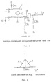
- FIG. 1 and FIG. 2 A typical circuit diagram of a prior art microwave voltage-controlled oscillator employing a GaAs FET and its noise characteristics are shown in FIG. 1 and FIG. 2, respectively and shown in the European Microwave Digest 1985 p407-412 "Wideband Tunable DR VCO" by Kenzo Wada, et al.
- Drain electrode D of a GaAs FET 14 is grounded, its gate electrode G is connected to a transmission line 13 whose opposite end is grounded via a DC (direct current) stopping capacitor C1 and a terminating resistor R1.
- An oscillation frequency signal f out is output from its source electrode S via a DC stopping capacitor C2.
- Transmission line 13 is electromagnetically coupled with a dielectric resonator 12 having a resonant frequency f o .
- Dielectric resonator 12 is further coupled with an open stub 11 whose one end is open and another end is connected to a variable-capacitance diode D1 to which a reverse bias is applied via a choke coil Ch1.
- Choke coils Ch2 and Ch3 supply a bias voltage to gate electrode G, and a source voltage to source electrode S, respectively.
- Open stub 11 and variable-capacitance diode D1 form a sub-resonator circuit and modulates, i.e. modifies, the resonant frequency f o of dielectric resonator 12 by the capacitance change according to the reverse voltage applied to the diode D1.
- the oscillator operates as a voltage-controlled oscillator providing a frequency change of, for example, ⁇ 30 MHz for 12 GHz centre frequency.
- GaAs FET 14 having worse low-frequency noise characteristics compared with that of a silicon transistor generates phase noise components denoted with A on the sidebands, namely ⁇ 1 MHZ, of the output frequency, 12 GHz, as shown as frequency spectrum in Fig. 2. Therefore, it has been seriously requested to provide a microwave voltage-controlled oscillator excellent in its phase-noise characteristics employing a transistor which is not good in a low-frequency noise characteristic.
- a voltage-controlled oscillator comprising: a transistor, a first terminal of said transistor being grounded, a second terminal of said transistor being connected to a resonator and an output signal being output from a third terminal of said transistor; and compensating means for detecting a low-frequency noise component generated in said transistor, characterized in that said detected low-frequency noise component is fed to a voltage-dependent reactance so as to cancel a phase-noise component included in said output signal of the voltage-controlled oscillator, and that a resonant frequency of said resonator is adjustable according to a voltage applied to said voltage-dependent reactance of said resonator.
- the above-described voltage-controlled oscillator may, in a preferred embodiment, be further provided with a reference crystal oscillator to which the voltage-controlled oscillator is phase-locked.
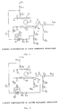
- a GaAs FET 5 is provided such that: drain electrode D is grounded, gate electrode G is connected to a transmission line 32 whose opposite end is grounded via a DC (direct current) stopping capacitor C1 and a terminating resistor R1 typically equivalent to the characteristic impedance of transmission line 32.
- An oscillation frequency signal frequency f out is output from its source electrode S via a DC stopping capacitor C2.
- Transmission line 32 typically formed of a strip line is electromagnetically coupled with a dielectric resonator 3 having a resonant frequency f o .
- Dielectric resonator 3 is further coupled with an open stub 21 whose one end is open and another end is connected to a variable-capacitance diode D1 to which a reverse bias +V V is applied via a resistor R10 and choke coil Ch1.
- Choke coil Ch2 supplies a bias voltage to gate electrode G
- choke coil Ch3 supplies source voltage to source electrode S, while the coke coils prevent the microwave signal.
- Open stub 21 and variable-capacitance diode D1 form a sub-resonator circuit and gives an effect on the resonant frequency f o of dielectric resonator 12 by the capacitance change according to the reverse voltage applied to the diode D1.
- the oscillation frequency is slightly deviated from the resonance frequency f o of dielectric resonator 3 by the diode voltage +V V .
- Electromagnetic couplings between transmission line 32 and dielectric resonator 3 and between the dielectric resonator 3 and open stub 21 are chosen so that the Q value of the oscillation circuit is kept high enough to stably maintain the oscillation frequency and at the same time the variable capacitance of diode D1 can adequately change the oscillation frequency.
- a low-frequency noise current flowing into gate electrode G generates a low-frequency noise voltage v nG , for example, 1 ⁇ V across a resistor R 2 typically of 1 k ⁇ connected between choke coil Ch 2 and gate bias voltage source -V G .
- Low-frequency noise voltage v nG is input via capacitor C3 and resistor R3 to amplifier 41 having capacitor C4 and resistor R4 both in parallel to amplifier 41, where the gain can be adjusted by the value of resistor R4 and capacitor C4.
- the output of amplifier 41 is negatively fed back via capacitor C5 and choke Ch1 to diode D1. Accordingly, the oscilation circuit, capacitor C3, resistor R3, amplifier 41, capacitor C5 and variable capacitance diode D1 constitute a negative feedback loop. Change in the oscillating frequency by the variable-capacitance diode is essentially equivalent to the change in the phase of the oscillating frequency.
- the adjustments of these feedback circuit elements are carried out so that the phase-noise component in the oscillated microwave signal becomes minimum. Power supply and ground circuit for amplifier 41 are omitted in the figures for simplification.
- FIG. 4 A second preferred embodiment of the present invention is shown in Fig. 4, where resistor R2 of Fig. 3 is replaced with resistor R7 typically of 10 ⁇ connected between source voltage source -V3 and choke coil Ch3.
- a voltage generated across resistor R7 is proportional to the drain current including the low-frequency current fluctuation.
- detected low-frequency noise voltage v nS is fed back via capacitor C3 and resistor R3 to amplifier 42 having capacitor C6 and resistor R6 both in parallel to amplifier 42, where phase of the output signal is inverted, capacitor C5 and choke Ch1 to diode D1.
- Function of the negative feedback loop is the same as that of Fig. 3 first preferred embodiment.
- a third preferred embodiment of the present invention is shown in Fig. 5, where the voltage-controlled oscillator 6 according to the first or second preferred embodiment is further phase-locked.
- Output of phase comparator 72 is input to a low-pass filter 74 having a cut-off frequency typically of 1 kHz which is the loop band width of the phase-locked loop.
- Output of low-pass filter 74 is added via a resistor R9 with the feedback signal supplied via resistor R8 from capacitor C5, so that the detected phase difference is negatively fed back to the diode D1, accordingly, the phase difference is kept zero.
- the output frequency is phase-locked to the reference frequency of crystal oscillator 8, as well as noise-compensated for the low-frequency noise.
- the output frequency can also be changed by modifying the number of frequency division N1 of the frequency divider 73.
- the output frequency can be frequency-modulated, namely phase-modulated, by a base band signal superposed onto the voltage applied to diode D1.
- the low-frequency noise component existing within ⁇ 1 MHz of the oscillation frequency is reduced by 10 db to 20 db.
Landscapes
- Inductance-Capacitance Distribution Constants And Capacitance-Resistance Oscillators (AREA)
- Stabilization Of Oscillater, Synchronisation, Frequency Synthesizers (AREA)
Claims (5)
- Spannungsgesteuerter Oszillator, mit einem Transistor (5), wobei ein erster Anschluß des Transistors auf Masse liegt, ein zweiter Anschluß des Transistors mit einem Resonator (3) verbunden ist und ein Ausgangssignal von einem dritten Anschluß des Transistors ausgegeben wird; und
Kompensationseinrichtungen zum Erfassen einer in dem Transistor erzeugten Niederfrequenz-Rauschkomponente, dadurch gekennzeichnet, daß die erfaßte Niederfrequenz Rauschkomponente in eine spannungsabhängige Reaktanz eingespeist wird, um eine in dem Ausgangssignal des spannungsgesteuerten Oszillators enthaltene Phasenrauschkomponente auszulöschen, und daß eine Resonanzfrequenz des Resonators gemäß einer an die spannungsabhängige Reaktanz (D₁) des Resonators angelegten Spannung abgleichbar ist. - Spannungsgesteuerter Oszillator nach Anspruch 1,
dadurch gekennzeichnet, daß der Transistor ein Galliumarsenid-Feldeffekttransistor ist. - Spannungsgesteuerter Oszillator nach Anspruch 1,
dadurch gekennzeichnet, daß der erste Anschluß eine Drainelektrode ist, der zweite Anschluß eine Gateelektrode und der dritte Anschluß eine Sourceelektrode ist. - Spannungsgesteuerter Oszillator nach Anspruch 1,
dadurch gekennzeichnet, daß die spannungsabhängige Reaktanz eine Diode variabler Kapazität ist, an welche eine Rückwärtsvorspannung angelegt wird, wobei die Diode variabler Kapazität elektromagnetisch mit dem Resonator gekoppelt ist. - Spannungsgesteuerter Oszillator nach Anspruch 1,
dadurch gekennzeichnet, daß die Kompensationseinrichtung ferner Phasenerfassungseinrichtungen(7) zum Erfassen einer Phasendifferenz zwischen der Phase der Ausgabe des spannungsgesteuerten Oszillators und der Phase einer Ausgabe eines Referenzoszillators (8) umfaßt, wobei die Spannung, die zu der spannungsabhängigen Reaktanz des Resonators zurückgeführt wird, gesteuert wird, die erfaßte Phasendifferenz im wesentlichen bei Null zu halten.
Applications Claiming Priority (2)
| Application Number | Priority Date | Filing Date | Title |
|---|---|---|---|
| JP2239625A JP2847573B2 (ja) | 1990-09-10 | 1990-09-10 | 電圧制御発振器 |
| JP239625/90 | 1990-09-10 |
Publications (2)
| Publication Number | Publication Date |
|---|---|
| EP0475262A1 EP0475262A1 (de) | 1992-03-18 |
| EP0475262B1 true EP0475262B1 (de) | 1994-03-16 |
Family
ID=17047507
Family Applications (1)
| Application Number | Title | Priority Date | Filing Date |
|---|---|---|---|
| EP91114919A Expired - Lifetime EP0475262B1 (de) | 1990-09-10 | 1991-09-04 | Spannungsgesteuerter Oszillator |
Country Status (4)
| Country | Link |
|---|---|
| US (1) | US5130675A (de) |
| EP (1) | EP0475262B1 (de) |
| JP (1) | JP2847573B2 (de) |
| DE (1) | DE69101417T2 (de) |
Families Citing this family (58)
| Publication number | Priority date | Publication date | Assignee | Title |
|---|---|---|---|---|
| US5233319A (en) * | 1992-03-27 | 1993-08-03 | The United States Of America As Represented By The Secretary Of The Army | Low-cost, low-noise, temperature-stable, tunable dielectric resonator oscillator |
| US5473287A (en) * | 1994-11-14 | 1995-12-05 | Micronetics, Inc. | Electronic oscillator with transmission line tuning of phase noise and linearity |
| US5748049A (en) * | 1994-11-23 | 1998-05-05 | Anadigics, Inc. | Multi-frequency local oscillators |
| US5568096A (en) * | 1995-04-19 | 1996-10-22 | Telefonaktiebolaget Lm Ericsson | Apparatus and method for using negative FM feedback in high quality oscillator devices |
| IT1277202B1 (it) * | 1995-06-30 | 1997-11-05 | Sits Soc It Telecom Siemens | Procedimento di stabilizzazione automatica della frequenza di oscillatore locale in radioricevitori impieganti un oscillatore |
| US5821827A (en) * | 1996-12-18 | 1998-10-13 | Endgate Corporation | Coplanar oscillator circuit structures |
| JPH10256905A (ja) * | 1997-03-14 | 1998-09-25 | Toshiba Corp | 位相同期回路装置 |
| US6064276A (en) * | 1998-06-16 | 2000-05-16 | Microware Solutions Limited | Oscillator circuit |
| GB2338617A (en) * | 1998-06-16 | 1999-12-22 | Microwave Solutions Limited | A voltage controlled oscillator with a dielectric resonator and a Schottky variable capacitance diode |
| JP3661573B2 (ja) * | 2000-07-24 | 2005-06-15 | 株式会社村田製作所 | 電圧制御発振器、電圧制御発振器装置およびレーダ装置 |
| US8749054B2 (en) | 2010-06-24 | 2014-06-10 | L. Pierre de Rochemont | Semiconductor carrier with vertical power FET module |
| JP4046567B2 (ja) * | 2002-07-29 | 2008-02-13 | 富士通テン株式会社 | 移動体検知装置 |
| FR2849725A1 (fr) * | 2003-01-06 | 2004-07-09 | Thomson Licensing Sa | Oscillateur a resonateur dielectrique commande en tension |
| US7196591B2 (en) | 2003-08-06 | 2007-03-27 | Synergy Microwave Corporation | Tunable frequency, low phase noise and low thermal drift oscillator |
| US7088189B2 (en) | 2003-09-09 | 2006-08-08 | Synergy Microwave Corporation | Integrated low noise microwave wideband push-push VCO |
| US7292113B2 (en) | 2003-09-09 | 2007-11-06 | Synergy Microwave Corporation | Multi-octave band tunable coupled-resonator oscillator |
| US7262670B2 (en) | 2003-12-09 | 2007-08-28 | Synergy Microwave Corporation | Low thermal drift, tunable frequency voltage controlled oscillator |
| JP4939228B2 (ja) * | 2003-12-09 | 2012-05-23 | シナジー マイクロウェーブ コーポレーション | 熱ドリフトがユーザ指定可能な電圧制御発振器 |
| EP1589655B1 (de) * | 2004-04-21 | 2019-08-21 | Synergy Microwave Corporation | Spannungsgesteuerter Breitbandozzillator mit gekoppelten Resonatoren vom Dämpfungstyp |
| EP1619789B1 (de) * | 2004-07-19 | 2019-09-11 | Synergy Microwave Corporation | Frequenzstimmbarer Oszillator mit niedriger Temperaturabweichung |
| CA2515982C (en) | 2004-08-16 | 2008-07-22 | Synergy Microwave Corporation | Low noise, hybrid tuned wideband voltage controlled oscillator |
| EP1797617A4 (de) | 2004-10-01 | 2009-08-12 | Rochemont L Pierre De | Keramisches antennenmodul und herstellungsverfahren dafür |
| EP1886403B1 (de) | 2005-05-20 | 2018-12-26 | Synergy Microwave Corporation | Einstellbarer oszillator mit serien- und parallelresonanzkreisen |
| US8715839B2 (en) | 2005-06-30 | 2014-05-06 | L. Pierre de Rochemont | Electrical components and method of manufacture |
| CA2566283C (en) | 2005-11-02 | 2011-10-18 | Synergy Microwave Corporation | User-definable, low cost, low phase hit and spectrally pure tunable oscillator |
| US7605670B2 (en) | 2005-11-15 | 2009-10-20 | Synergy Microwave Corporation | User-definable low cost, low noise, and phase hit insensitive multi-octave-band tunable oscillator |
| US8354294B2 (en) * | 2006-01-24 | 2013-01-15 | De Rochemont L Pierre | Liquid chemical deposition apparatus and process and products therefrom |
| US7959598B2 (en) | 2008-08-20 | 2011-06-14 | Asante Solutions, Inc. | Infusion pump systems and methods |
| US8952858B2 (en) | 2009-06-17 | 2015-02-10 | L. Pierre de Rochemont | Frequency-selective dipole antennas |
| US8922347B1 (en) | 2009-06-17 | 2014-12-30 | L. Pierre de Rochemont | R.F. energy collection circuit for wireless devices |
| US8552708B2 (en) | 2010-06-02 | 2013-10-08 | L. Pierre de Rochemont | Monolithic DC/DC power management module with surface FET |
| US9023493B2 (en) | 2010-07-13 | 2015-05-05 | L. Pierre de Rochemont | Chemically complex ablative max-phase material and method of manufacture |
| CN109148425B (zh) * | 2010-08-23 | 2022-10-04 | L·皮尔·德罗什蒙 | 具有谐振晶体管栅极的功率场效应晶体管 |
| CN103415925A (zh) | 2010-11-03 | 2013-11-27 | L·皮尔·德罗什蒙 | 具有单片集成的量子点器件的半导体芯片载体及其制造方法 |
| TW201401762A (zh) * | 2012-06-27 | 2014-01-01 | Yong-Sheng Huang | 降低振盪器相位雜訊的電路 |
| US9561324B2 (en) | 2013-07-19 | 2017-02-07 | Bigfoot Biomedical, Inc. | Infusion pump system and method |
| US10275573B2 (en) | 2016-01-13 | 2019-04-30 | Bigfoot Biomedical, Inc. | User interface for diabetes management system |
| HK1256995A1 (zh) | 2016-01-14 | 2019-10-11 | Bigfoot Biomedical, Inc. | 药物输送设备、系统和方法中的阻塞解决方案 |
| US10806859B2 (en) | 2016-01-14 | 2020-10-20 | Bigfoot Biomedical, Inc. | Adjusting insulin delivery rates |
| US12383166B2 (en) | 2016-05-23 | 2025-08-12 | Insulet Corporation | Insulin delivery system and methods with risk-based set points |
| US10363374B2 (en) | 2016-05-26 | 2019-07-30 | Insulet Corporation | Multi-dose drug delivery device |
| CA3037432A1 (en) | 2016-12-12 | 2018-06-21 | Bigfoot Biomedical, Inc. | Alarms and alerts for medication delivery devices and related systems and methods |
| US10547096B2 (en) | 2016-12-22 | 2020-01-28 | Knowles Cazenovia, Inc. | Microwave cavity resonator stabilized oscillator |
| US10500334B2 (en) | 2017-01-13 | 2019-12-10 | Bigfoot Biomedical, Inc. | System and method for adjusting insulin delivery |
| US10758675B2 (en) | 2017-01-13 | 2020-09-01 | Bigfoot Biomedical, Inc. | System and method for adjusting insulin delivery |
| EP3568860B1 (de) | 2017-01-13 | 2025-12-10 | Insulet Corporation | Insulinverabreichungsverfahren, -systeme und -vorrichtungen |
| US10881793B2 (en) | 2017-01-13 | 2021-01-05 | Bigfoot Biomedical, Inc. | System and method for adjusting insulin delivery |
| EP4708311A2 (de) | 2017-01-13 | 2026-03-11 | Insulet Corporation | Insulinverabreichungsverfahren, -systeme und -vorrichtungen |
| US10583250B2 (en) | 2017-01-13 | 2020-03-10 | Bigfoot Biomedical, Inc. | System and method for adjusting insulin delivery |
| USD874471S1 (en) | 2017-06-08 | 2020-02-04 | Insulet Corporation | Display screen with a graphical user interface |
| USD928199S1 (en) | 2018-04-02 | 2021-08-17 | Bigfoot Biomedical, Inc. | Medication delivery device with icons |
| US12562251B1 (en) | 2018-05-09 | 2026-02-24 | Bigfoot Biomedical, Inc. | Computing architecture for assuring the provenance of medication therapy related parameters, and related systems, methods and devices |
| USD920343S1 (en) | 2019-01-09 | 2021-05-25 | Bigfoot Biomedical, Inc. | Display screen or portion thereof with graphical user interface associated with insulin delivery |
| USD977502S1 (en) | 2020-06-09 | 2023-02-07 | Insulet Corporation | Display screen with graphical user interface |
| JP7665028B2 (ja) | 2020-12-18 | 2025-04-18 | インスレット コーポレイション | 薬物送達デバイスによる将来の日付および時刻における薬物ボーラス送達の、コンピューティングデバイスを用いたスケジュール設定 |
| US12514980B2 (en) | 2021-06-30 | 2026-01-06 | Insulet Corporation | Adjustment of medicament delivery by a medicament delivery device based on menstrual cycle phase |
| US12521486B2 (en) | 2021-07-16 | 2026-01-13 | Insulet Corporation | Method for modification of insulin delivery during pregnancy in automatic insulin delivery systems |
| CN120457493A (zh) | 2023-01-06 | 2025-08-08 | 英赛罗公司 | 自动或手动启动的随餐推注输送及随后的自动安全约束放宽 |
Family Cites Families (2)
| Publication number | Priority date | Publication date | Assignee | Title |
|---|---|---|---|---|
| US4630004A (en) * | 1985-04-11 | 1986-12-16 | The United States Of America As Represented By The Secretary Of The Air Force | Dielectric resonator stabilized microstrip oscillator |
| FR2595518A1 (fr) * | 1986-03-07 | 1987-09-11 | Thomson Csf | Oscillateur a faible bruit aux environs de sa frequence d'oscillation |
-
1990
- 1990-09-10 JP JP2239625A patent/JP2847573B2/ja not_active Expired - Lifetime
-
1991
- 1991-09-04 EP EP91114919A patent/EP0475262B1/de not_active Expired - Lifetime
- 1991-09-04 DE DE69101417T patent/DE69101417T2/de not_active Expired - Fee Related
- 1991-09-04 US US07/754,826 patent/US5130675A/en not_active Expired - Fee Related
Non-Patent Citations (1)
| Title |
|---|
| 15th European Microwave Conference, September 1985, Paris, France, "Wideband tunable DR VCO" pages 407-412, K. Wada et al. * |
Also Published As
| Publication number | Publication date |
|---|---|
| DE69101417T2 (de) | 1994-07-14 |
| DE69101417D1 (de) | 1994-04-21 |
| JPH04119705A (ja) | 1992-04-21 |
| EP0475262A1 (de) | 1992-03-18 |
| US5130675A (en) | 1992-07-14 |
| JP2847573B2 (ja) | 1999-01-20 |
Similar Documents
| Publication | Publication Date | Title |
|---|---|---|
| EP0475262B1 (de) | Spannungsgesteuerter Oszillator | |
| US5231361A (en) | Voltage controlled push-push oscillator with parallel resonant tank circuits | |
| US5942950A (en) | Varactor tuned strip line resonator and VCO using same | |
| US6466099B2 (en) | Voltage controlled oscillator (VCO) in colpitts configuration | |
| US4926144A (en) | Multi-function modulation and center frequency control port for voltage controlled oscillator | |
| US4375621A (en) | Circuit for linearizing frequency modulated oscillators on microstrip | |
| US5565821A (en) | Voltage controlled oscillator with improved tuning linearity | |
| US4088968A (en) | Frequency linearization and sensitivity equalization of a frequency modulated crystal oscillator | |
| KR20040012852A (ko) | 광대역 전압 제어형 수정 발진기 | |
| US4189690A (en) | Resonant linear frequency modulator | |
| US5027429A (en) | Frequency modulator utilizing frequency synthesizer | |
| US4737737A (en) | Transmission injection-locked dielectric resonator oscillator | |
| US5138285A (en) | Method for reducing phase noise in oscillators | |
| US7330083B2 (en) | Oscillator having voltage dividing circuit | |
| CA2071817C (en) | High-frequency voltage controlled oscillator | |
| US3982211A (en) | Linearized varactor frequency modulated semi-conductor diode oscillator | |
| US5838207A (en) | Voltage controlled oscillator with partial load-pull tuning | |
| US5159293A (en) | Voltage-controlled oscillator with wide modulation bandwidth | |
| CA1206540A (en) | Single-stage oscillator having low-impedance feedback port | |
| EP1188227B1 (de) | Spannungsgesteuerter oszillator | |
| US6075421A (en) | Voltage controlled oscillator | |
| US6172577B1 (en) | Oscillator and oscillation apparatus using the oscillator | |
| US4743865A (en) | Quartz-crystal microwave oscillator of the common-emitter transmission type with two transistors and a predetermined loaded Q factor | |
| US4630008A (en) | Direct FM crystal-controlled oscillator | |
| EP0267332A1 (de) | Direkt frequenzmodulierter, kristallgesteuerter Oszillator |
Legal Events
| Date | Code | Title | Description |
|---|---|---|---|
| PUAI | Public reference made under article 153(3) epc to a published international application that has entered the european phase |
Free format text: ORIGINAL CODE: 0009012 |
|
| AK | Designated contracting states |
Kind code of ref document: A1 Designated state(s): DE FR GB |
|
| 17P | Request for examination filed |
Effective date: 19920224 |
|
| 17Q | First examination report despatched |
Effective date: 19920623 |
|
| GRAA | (expected) grant |
Free format text: ORIGINAL CODE: 0009210 |
|
| AK | Designated contracting states |
Kind code of ref document: B1 Designated state(s): DE FR GB |
|
| REF | Corresponds to: |
Ref document number: 69101417 Country of ref document: DE Date of ref document: 19940421 |
|
| ET | Fr: translation filed | ||
| PLBE | No opposition filed within time limit |
Free format text: ORIGINAL CODE: 0009261 |
|
| STAA | Information on the status of an ep patent application or granted ep patent |
Free format text: STATUS: NO OPPOSITION FILED WITHIN TIME LIMIT |
|
| 26N | No opposition filed | ||
| PGFP | Annual fee paid to national office [announced via postgrant information from national office to epo] |
Ref country code: GB Payment date: 19990901 Year of fee payment: 9 |
|
| PGFP | Annual fee paid to national office [announced via postgrant information from national office to epo] |
Ref country code: DE Payment date: 19990906 Year of fee payment: 9 |
|
| PGFP | Annual fee paid to national office [announced via postgrant information from national office to epo] |
Ref country code: FR Payment date: 19990909 Year of fee payment: 9 |
|
| PG25 | Lapsed in a contracting state [announced via postgrant information from national office to epo] |
Ref country code: GB Free format text: LAPSE BECAUSE OF NON-PAYMENT OF DUE FEES Effective date: 20000904 |
|
| GBPC | Gb: european patent ceased through non-payment of renewal fee |
Effective date: 20000904 |
|
| PG25 | Lapsed in a contracting state [announced via postgrant information from national office to epo] |
Ref country code: FR Free format text: LAPSE BECAUSE OF NON-PAYMENT OF DUE FEES Effective date: 20010531 |
|
| PG25 | Lapsed in a contracting state [announced via postgrant information from national office to epo] |
Ref country code: DE Free format text: LAPSE BECAUSE OF NON-PAYMENT OF DUE FEES Effective date: 20010601 |
|
| REG | Reference to a national code |
Ref country code: FR Ref legal event code: ST |