EP0475365A2 - Méthode d'asservissement pour appareil de mémorisation - Google Patents
Méthode d'asservissement pour appareil de mémorisation Download PDFInfo
- Publication number
- EP0475365A2 EP0475365A2 EP91115305A EP91115305A EP0475365A2 EP 0475365 A2 EP0475365 A2 EP 0475365A2 EP 91115305 A EP91115305 A EP 91115305A EP 91115305 A EP91115305 A EP 91115305A EP 0475365 A2 EP0475365 A2 EP 0475365A2
- Authority
- EP
- European Patent Office
- Prior art keywords
- recording medium
- probe
- bit line
- information bit
- scanning
- Prior art date
- Legal status (The legal status is an assumption and is not a legal conclusion. Google has not performed a legal analysis and makes no representation as to the accuracy of the status listed.)
- Granted
Links
Images


Classifications
-
- G—PHYSICS
- G11—INFORMATION STORAGE
- G11B—INFORMATION STORAGE BASED ON RELATIVE MOVEMENT BETWEEN RECORD CARRIER AND TRANSDUCER
- G11B9/00—Recording or reproducing using a method not covered by one of the main groups G11B3/00 - G11B7/00; Record carriers therefor
- G11B9/12—Recording or reproducing using a method not covered by one of the main groups G11B3/00 - G11B7/00; Record carriers therefor using near-field interactions; Record carriers therefor
- G11B9/14—Recording or reproducing using a method not covered by one of the main groups G11B3/00 - G11B7/00; Record carriers therefor using near-field interactions; Record carriers therefor using microscopic probe means, i.e. recording or reproducing by means directly associated with the tip of a microscopic electrical probe as used in Scanning Tunneling Microscopy [STM] or Atomic Force Microscopy [AFM] for inducing physical or electrical perturbations in a recording medium; Record carriers or media specially adapted for such transducing of information
- G11B9/1418—Disposition or mounting of heads or record carriers
- G11B9/1427—Disposition or mounting of heads or record carriers with provision for moving the heads or record carriers relatively to each other or for access to indexed parts without effectively imparting a relative movement
- G11B9/1436—Disposition or mounting of heads or record carriers with provision for moving the heads or record carriers relatively to each other or for access to indexed parts without effectively imparting a relative movement with provision for moving the heads or record carriers relatively to each other
-
- B—PERFORMING OPERATIONS; TRANSPORTING
- B82—NANOTECHNOLOGY
- B82Y—SPECIFIC USES OR APPLICATIONS OF NANOSTRUCTURES; MEASUREMENT OR ANALYSIS OF NANOSTRUCTURES; MANUFACTURE OR TREATMENT OF NANOSTRUCTURES
- B82Y10/00—Nanotechnology for information processing, storage or transmission, e.g. quantum computing or single electron logic
-
- G—PHYSICS
- G11—INFORMATION STORAGE
- G11B—INFORMATION STORAGE BASED ON RELATIVE MOVEMENT BETWEEN RECORD CARRIER AND TRANSDUCER
- G11B11/00—Recording on or reproducing from the same record carrier wherein for these two operations the methods are covered by different main groups of groups G11B3/00 - G11B7/00 or by different subgroups of group G11B9/00; Record carriers therefor
- G11B11/08—Recording on or reproducing from the same record carrier wherein for these two operations the methods are covered by different main groups of groups G11B3/00 - G11B7/00 or by different subgroups of group G11B9/00; Record carriers therefor using recording by electric charge or by variation of electric resistance or capacitance
-
- G—PHYSICS
- G11—INFORMATION STORAGE
- G11B—INFORMATION STORAGE BASED ON RELATIVE MOVEMENT BETWEEN RECORD CARRIER AND TRANSDUCER
- G11B17/00—Guiding record carriers not specifically of filamentary or web form, or of supports therefor
- G11B17/34—Guiding record carriers during transducing operation, e.g. for track following
-
- G—PHYSICS
- G11—INFORMATION STORAGE
- G11B—INFORMATION STORAGE BASED ON RELATIVE MOVEMENT BETWEEN RECORD CARRIER AND TRANSDUCER
- G11B21/00—Head arrangements not specific to the method of recording or reproducing
- G11B21/02—Driving or moving of heads
- G11B21/10—Track finding or aligning by moving the head ; Provisions for maintaining alignment of the head relative to the track during transducing operation, i.e. track following
-
- Y—GENERAL TAGGING OF NEW TECHNOLOGICAL DEVELOPMENTS; GENERAL TAGGING OF CROSS-SECTIONAL TECHNOLOGIES SPANNING OVER SEVERAL SECTIONS OF THE IPC; TECHNICAL SUBJECTS COVERED BY FORMER USPC CROSS-REFERENCE ART COLLECTIONS [XRACs] AND DIGESTS
- Y10—TECHNICAL SUBJECTS COVERED BY FORMER USPC
- Y10S—TECHNICAL SUBJECTS COVERED BY FORMER USPC CROSS-REFERENCE ART COLLECTIONS [XRACs] AND DIGESTS
- Y10S977/00—Nanotechnology
- Y10S977/902—Specified use of nanostructure
- Y10S977/932—Specified use of nanostructure for electronic or optoelectronic application
- Y10S977/943—Information storage or retrieval using nanostructure
- Y10S977/947—Information storage or retrieval using nanostructure with scanning probe instrument
Definitions
- the present invention relates to a very high density memory apparatus which employs the principle of the SUM (Scanning Tunneling Microscope) which is capable of measuring atomic level irregularities by detecting a tunnel current.
- SUM Sccanning Tunneling Microscope
- a high resolution microscope called a "STM" (Scanning Tunnel Microscope) capable of directly observing atoms present on the surface of the conductor has been developed [G. Binning et al., Helvetica Physica Acta, 55, 726 (1982)].
- STM Scnning Tunnel Microscope
- the STM exhibits an advantage in that the subject can be observed at reduced energy while eliminating a risk of damaging the medium by an electric current.
- the STM is able to operate in an atmosphere and to be applied to various materials, the STM is expected to be widely used.
- the STM is arranged to utilize a fact that a tunnel current flows when a voltage is applied between a probe (a probe electrode) and a conductive material which are caused to come closer to each other to a distance about 1 nm. Since the tunnel current is very sensitive to the change in the distance between the probe electrode and the conductive material, the surface structure of the real space can be drawn by scanning the probe electrode in such a manner that the tunnel current is maintained at a constant value. Simultaneously, various informations concerning all electron clouds of the surface atoms can be read out. At this time, the resolution in an in-plane direction is about 1 ⁇ . Therefore, by utilizing the principle of the STM, desired high density recording/reproducing can be performed in the atomic order (several ⁇ ).
- the recording/reproducing method a method has been proposed in which the surface status of an appropriate recording layer is changed by using corpuscular beams (electron beams or ion beams), high energy electromagnetic wave such as X-rays or energy beams such as visible or ultra-violet rays to thereby perform recording.
- corpuscular beams electron beams or ion beams
- high energy electromagnetic wave such as X-rays or energy beams such as visible or ultra-violet rays
- the STM is used to reproduce data.
- Another method has been proposed in which a material having an effect of memorizing the switching characteristics of an electric current, for example, a conjugate ⁇ electronic organic compound or a material containing chalcogen is used to form a thin layer so as to perform recording/reproducing by the STM.
- the tracking can be performed by a method in which the atomic arrangement of the recording medium is utilized to form the tracking signal to perform scanning with a probe electrode. Another method can be available in which a track is previously formed in the surface of the recording medium. Furthermore, an wobbling method can be employed in which the probe electrode is finely vibrated in the widthwise direction of the information bit line. In particular, the wobbling method is very simple and convenient in comparison to the other methods because the tracking signal can be generated from the reproduce signal of information.
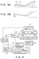
- the probe electrode when recorded information bit line is scanned to read a reproduce signal, the probe electrode is stationarily vibrated at frequency f with an amplitude smaller than the width of the bit line, in a direction perpendicular to the bit line.
- the frequency f is set to a value sufficiently large with respect to the frequency of the reproduce signal of the bit line.
- the envelope of the reproduce signal of the bit line is, as shown in Fig. 1B, changed as designated by signals b , c and d shown in Fig. 1B depending on the positions shown by the arrows given by same symbols in Fig. 1A. Therefore, by taking the signals denoting the changes in the envelope, signals b ', c ' and d ' shown in Fig. 1B can be obtained. That is, the envelope change signal with respect to vibration waveform a of the probe electrode is reduced as designated by signal c ', when the probe electrode is positioned above the bit line as designated by arrow c .
- the amplitude is enlarged while the phase is displaced by 180° with respect to the vibration waveform a of the probe electrode.
- the amplitude is enlarged with the same phase as that of the vibration waveform a of the probe electrode. Therefore, by performing a phase detection operation using the normal signal of frequency f of the probe electrode as a reference signal, a tracking signal in proportion to the displacement quantity from the bit line can be obtained. As a result, a feedback control in which the probe electrode is maintained at a position above the bit column, can be performed by using the tracking signal.
- wobbling frequency f must be higher than the offtrack frequency component in order to stably perform the tracking.
- an object of the present invention is to provide an information recording apparatus and a method therefor capable of generating tracking information from a reproduce signal without wobbling and scanning information bit line with high accuracy when a probe electrode is scanned on the information bit line formed on a recording medium.
- a detection signal of the probe includes a reproduce signal.
- the amplitude of the information bit signal component of the detection signal becomes large when the probe correctly tracks the information bit line on the recording medium.
- the amplitude becomes small when the probe deviates from the information bit line. Therefore, according to an aspect of the present invention, the probe position is controlled in a direction in which the above-described amplitude is, for example, enlarged, whereby tracking can always correctly be performed.
- two times of preliminary scanning operations are performed in relation to one signal line upon reproducing operation.
- the physical quantity in relation to the recording medium detected by the probe is used to detect the displacement between the central position of the signal line and the preliminary scanning position. Then, the recording/reproducing scanning operation is performed in accordance with the displacement thus-detected.
- Fig. 2 is a block diagram which illustrates the structure of the first embodiment of a memory apparatus according to the present invention.
- the memory apparatus according to this embodiment comprises: a probe electrode 2; tracking means (not shown) for causing the probe electrode 2 to face the surface of a recording medium having information lines, which has been sequentially recorded as pits and projections on the surface or changes in the electronic states, to relatively travel along the information line; voltage applying means (not shown) for applying voltage between a recording medium 1 and the probe electrode 2 to generate a tunnel current; a bias voltage source 4, a resistor R, an amplifier 5 and a signal processing circuit 6 for converting the tunnel current signal into a voltage signal to reproduce informations recorded on the recording medium 1; a detection circuit 7 for detecting the change in the intensity of an envelope signal of the tunnel current signal which has been converted into the voltage signal output from the amplifier 5; two sample hold circuits 8; comparator 9; microcomputer 10; and piezoelectric ceramics 15 for finely moving the probe electrode 2 in an intersecting direction (perpendic
- the recording medium 1 is illustrated by its cross section in a direction perpendicular to the record bit line.
- the recording medium 1 may be made of a material having the current and voltage characteristics which shows a memory switching phenomenon, i.e., a material showing a phenomenon of reversible transition in the electrical conductivity, the material being formed on a conductive substrate.
- an amorphous semiconductor such as oxide glass, borate glass, or chalcogenide glass containing Se, Te or As combined with an element of III, IV, V or VI group of the periodic table; an organic compound having a group with conjugated ⁇ electronic level and a group with ⁇ electronic level in the molecule thereof; a coloring matter having a porphin skeleton such as phthalocyanine or tetraphenylporphin; as azulene coloring matter having a squalillyum base and a chroconic base as a bonding chain; a coloring matter like a cyanine in which two heterocycles including nitrogen such as quinoline, benzothiazole and benzo-oxazole are bonded to each other by the a squalillyum base and a chroconic base; a cyanine coloring matter, a condensed polycyclic aromatic group such as anthracene and pyrene, a chain compound in which an aromatic
- the above-described material is used in the form of a monomolecular film or a built-up film. It is preferable to employ a so-called Langmuir-Blodgett's (LB) method in which in order to form the monomolecular film or the built-up film of the organic compound an amphipathic material is molecular-oriented at a high density on the water level to form a monomolecular film, the molecular film being then transcribed onto the substrate.
- LB Langmuir-Blodgett's
- the recording medium 1 is constituted by laminating a base layer made of Au and a recording layer made of amorphous Si containing hydrogen by 30 atom% on a glass substrate.
- the probe electrode 2 have an end portion sharpened as much as possible by etching or electropolishing.
- the probe electrode 2 is produced in such a manner that a rod of tungsten having a diameter of 1 mm ⁇ is mechanically polished to form into a conical shape having an angle of 90°, and then an electric field is applied to the same under ultra high vacuum to evaporate the surface atoms.
- the present invention is not limited to the above-described shape, the producing method and the material of the probe electrode 2.
- the distance from the recording medium 1 to the probe electrode 2 serving as a pickup must be the distance which enables a tunnel current generated due to the tunnel effect to be detected.
- the distance from the probe electrode 2 to the recording medium 1 and their relative position are controlled by an actuator 12.
- the actuator 12 comprises a fixed base 13, a movable base 16 and piezoelectric ceramics 14 and 15 such as a PLZT or a PZT.
- the movable base 16 is connected to the probe electrode 2.
- control voltage is applied to the same to extend/contact the piezoelectric ceramics 14 and 15 the probe electrode 2 can be moved in Z direction (vertical direction) or XY direction (lateral direction) with respect to the recording medium 1.
- Informations can be recorded on the recording medium 1 by using the apparatus thus-constituted in such a manner that writing pulse voltage having the wave height value of which is 5 V and the pulse width of which is 1 ⁇ sec is applied to the probe electrode 2 to pass the tunnel current to the recording position when a switch 3 is switched on as shown in Fig. 2 and the probe electrode 2 is moved.
- record bits having the diameter of each of which is about 10 nm are formed on a straight line at a pitch of 15 nm.
- the distance from the probe electrode 2 and the recording medium 1 is set in order to obtain the tunnel current in the control circuit 11.
- the tunnel current passing through the probe electrode 2 changes in accordance with the record bits (curve TN shown in Fig. 3A).
- a curve EV shown in Fig. 3A shows the envelope of the above-described tunnel current signal. It can be considered that the increase/decrease of the absolute value of the envelope substantially coincides with incresae/decrease in the amplitude of a signal (information bit signal component) which corresponds to the recording bits.
- the above-described signal current is I-V transformed through the resistor R and then it is amplified by the amplifier 5.
- the output from the amplifier 5 is supplied to the signal processing circuit 6 so that reproduction information of "ON” or "OFF” is obtained.
- the output from the amplifier 5 is also supplied to the detection circuit 7 in which the reproduce signal is envelope-detected before supplied to the two sample hold circuits 8.
- Each of the sample hold circuits 8 alternately updates the envelope absolute values by using sample pulses transmitted from the microcomputer 10.
- the envelop absolute values are sequentially subjected to comparisons by the comparator 9.
- Fig. 3B illustrates an example of each of outputs S1 and S2 from the corresponding sample hold circuits 8. The result of the comparison is taken in into the microcomputer 10 to discriminate the direction of the voltage to be applied to the piezoelectric ceramics 15, so that proper voltage is transmitted to the piezoelectric ceramics 15.
- the voltage level to be applied is changed, for example, increased to be subjected to a comparison with the next sampling envelope. If the sampling envelope absolute value (level) of the updated circuit is higher than the sampling envelope level of the other circuit, the level of the applied voltage is allowed to increase (if the same is lower, the voltage level is decreased to be subjected to a comparison with the next sampling envelope. Then, until the update side envelope level is decreased in comparison with that of the opposite side sample (until the same is increased in the contrary case) the applied voltage is changed in the same direction, that is, the probe electrode 2 is displaced in the same direction.
- control voltage is applied to the piezoelectric ceramics 15 to control the lateral directional position of the probe electrode 2 so that the envelope level of the reproduce signal becomes the maximum level, whereby the probe electrode 2 is positioned at the most suitable position in the stable state and the tracking can be automatically performed.
- the period of the sampling pulse is set to be longer than the period of the information bits, and the voltage displacement per step to be supplied from the microcomputer 10 to the piezoelectric ceramics 15 is set to be 1 nm, whereby the envelope level of the reproduce signal can be brought into a stable state and the tracking can be performed with an accuracy of ⁇ 1 nm.
- envelope level is used in the above-described embodiment, another method may be employed in which the amplitude of the information bit signal component is directly detected and the probe position is controlled in the direction in which the amplitude thus-detected is enlarged. Furthermore, tracking may be performed by driving the portion including the recording medium 1.
- tracking information can be generated from the reproduce signal without wobbling. Therefore, an advantage can be obtained in that information can be read out with excellent reproducibility.
- Fig. 4 is structural view which illustrates a memory apparatus according to this embodiment.
- a recording medium 23 on to which a base electrode 22 is fixed is placed on an XY major moving mechanism 21 mainly composed of parallel springs made of elastic hinges and capable of coarsely moving on the XY plane.
- a probe electrode 25 fixed to a three-dimensional fine moving mechanism 24 made of a piezoelectric element is disposed above the recording medium 23.
- a voltage application circuit 26 and a current detection circuit 27 are connected to the recording medium 23 and the probe electrode 25.
- the voltage application circuit 26 and the current detection circuit 27 are connected to a microcomputer 28.
- the output from the current detection circuit 27 is transmitted to integrators 29a and 29b.
- the outputs from the integrators 29a and 29b are transmitted to a differential circuit 31 through hold circuits 30a and 30b, respectively.
- the output from the differential circuit 31 is transmitted to a drive circuit 32 which is connected to the XY major moving mechanism 21, the 3-D fine moving mechanism 24 and the microcomputer 28.
- the probe electrode 25 may be used in which the edge portion of pin of tungsten, Pt-Ir, Pt, or the like is mechanically polished and then is electrolytic polished.
- the recording medium 23 is produced in such a manner that a material similar to those in the first embodiment having a memory effect in relation to switching characteristics of the voltage current is used in, for example, the Langmuir's-Blodgetts (LB) method so that four layers of squalillyum-bis-6-octyl azulene are formed on a graphite substrate.
- LB Langmuir's-Blodgetts
- the XY major moving mechanism 21 and the 3-D fine moving mechanism 24 are driven by the microcomputer 28 and the drive circuit 32, so that the positional relationship between the recording medium 23 and the probe electrode 25 is coarsely set.
- the XY major moving mechanism 21 and the 3-D fine moving mechanism 24 are driven by the drive circuit 32, so that the probe electrode 25 is relatively scanned above the surface of the recording medium 23. Then, the pulse voltage is applied between the probe electrode 25 and the recording medium 23 by the voltage application circuit 26. As a result, portions having different electric resistance levels are locally created on the surface of the recording medium 23 to perform recording.
- the tracking control is performed in a method to be described later while a constant voltage is applied to such a degree that the tunnel current flows between the probe electrode 25 and the recording medium 23, so that the data lines formed on the recording medium 23 are scanned by the probe electrode 25.
- the tunnel current obtained at the above-described scanning operation is detected by the current detection circuit 27.
- the 3-D fine moving mechanism 24 is driven by the drive circuit 32 so that the average value of the tunnel current becomes a substantially constant value, whereby the probe electrode 25 is vertically moved. Since the distance of the vertical movement at this time corresponds to recorded informations, reproducing data is generated in accordance with the distance of the vertical movement.
- the signal line is preliminarily scanned two times for tracking the signal line.
- the detection signal obtained by the preliminary scanning is used to perform third recording/reproducing tracking.
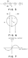
- Fig. 5 illustrates signal line L, first and second preliminary scanning loci M1 and M2.
- the two times of preliminary scanning operations are performed in parallel at an interval smaller than the diameter of recording bit B of the signal line L so that the two preliminary scanning loci M1 and M2 pass on the signal line L.
- the tunnel currents detected by the current detection circuit 27 at the time of the first and second preliminary scanning operations are integrated by integrators 29a and 29b, respectively.
- the integration results Ia and Ib are held by hold circuits 30a and 30b.
- Fig. 6 illustrates an example of each of the two preliminary scanning loci M1 and M2.
- Fig. 7 illustrates the relationship between the displacement of the preliminary scanning loci M1 and M2 in relation to the record bit B and the differential output from the differential circuit 11.
- the differential output becomes 0. If the intermediate position between the two preliminary scanning loci M1 and M2 is displaced to the right with respect to the record bit B, the integration result Ia increases and the integration result Ib decreases. As a result, the differential output increases. If the intermediate position is displaced to the left, the integration Ia decreases and Ib increases.
- the interval between the two preliminary scanning loci M1 and M2 is a known value
- the displacement between the intermediate position between the two preliminary scanning loci M1, M2 and the center O of the actual record bit B can be detected from the differential output.
- the probe electrode 25 can be controlled so as to pass near the central position of the signal line L.
- the hold circuits 30a and 30b are reset before the next pre-scanning operation is performed, so that the influence of the previous scanning operation can be eliminated.
- the number of times of the preliminary scanning operations to be performed is not limited to the two times.
- the pre-scanning operations may be performed plural times, for example, three or more times.
- the present invention can be adapted to an apparatus capable of performing only the recording operation or that capable of performing only the reproducing operation.
- the tracking method according to this embodiment is arranged in such a manner that one signal line is subjected to, for example, two times of preliminary scanning operations at the time of the reproducing operation.
- the physical quantity of the recording medium detected by the probe is used to detect the displacement between the central position of the signal line and the preliminary scanning position. Since the recording/reproducing scanning operation is performed in accordance with the displacement thus-detected, the tracking accuracy can be improved and the S/N ratio at the time of the reproducing operation can be improved. Furthermore, the reliability of the reproduce signal can be improved.
Landscapes
- Engineering & Computer Science (AREA)
- Chemical & Material Sciences (AREA)
- Nanotechnology (AREA)
- Physics & Mathematics (AREA)
- Mathematical Physics (AREA)
- Theoretical Computer Science (AREA)
- Crystallography & Structural Chemistry (AREA)
- Measurement Of Length, Angles, Or The Like Using Electric Or Magnetic Means (AREA)
- Length Measuring Devices With Unspecified Measuring Means (AREA)
- Warehouses Or Storage Devices (AREA)
- Radar Systems Or Details Thereof (AREA)
- Optical Recording Or Reproduction (AREA)
Applications Claiming Priority (4)
| Application Number | Priority Date | Filing Date | Title |
|---|---|---|---|
| JP24277590A JPH04123338A (ja) | 1990-09-14 | 1990-09-14 | 情報再生装置および方法 |
| JP242775/90 | 1990-09-14 | ||
| JP15762591A JP2930449B2 (ja) | 1991-05-31 | 1991-05-31 | トラッキング方法 |
| JP157625/90 | 1991-05-31 |
Publications (3)
| Publication Number | Publication Date |
|---|---|
| EP0475365A2 true EP0475365A2 (fr) | 1992-03-18 |
| EP0475365A3 EP0475365A3 (en) | 1992-10-07 |
| EP0475365B1 EP0475365B1 (fr) | 1997-04-09 |
Family
ID=26485009
Family Applications (1)
| Application Number | Title | Priority Date | Filing Date |
|---|---|---|---|
| EP91115305A Expired - Lifetime EP0475365B1 (fr) | 1990-09-14 | 1991-09-10 | Méthode d'asservissement pour appareil de mémorisation |
Country Status (5)
| Country | Link |
|---|---|
| US (1) | US5251200A (fr) |
| EP (1) | EP0475365B1 (fr) |
| AT (1) | ATE151557T1 (fr) |
| CA (1) | CA2051192C (fr) |
| DE (1) | DE69125552T2 (fr) |
Cited By (1)
| Publication number | Priority date | Publication date | Assignee | Title |
|---|---|---|---|---|
| EP0518240A3 (en) * | 1991-06-11 | 1995-02-22 | Canon Kk | Information reproducing method and information reproducing apparatus which uses the method |
Families Citing this family (19)
| Publication number | Priority date | Publication date | Assignee | Title |
|---|---|---|---|---|
| JPH041948A (ja) * | 1990-04-18 | 1992-01-07 | Canon Inc | 情報記録装置及び情報再生装置及び情報記録再生装置 |
| WO2004081684A1 (fr) * | 1991-11-29 | 2004-09-23 | Ryuji Takada | Procede et appareil pour commander un dispositif piezo-electrique, et controleur de micromanipulateur |
| EP0558177B1 (fr) * | 1992-01-29 | 2000-04-12 | Advanced Micro Devices, Inc. | Système de microscope à émission resolvant d'énergie et procédé |
| JPH06251435A (ja) * | 1993-03-01 | 1994-09-09 | Canon Inc | 記録再生装置 |
| JP3135753B2 (ja) * | 1993-08-26 | 2001-02-19 | キヤノン株式会社 | プローブを用いた記録再生方法および装置 |
| JP3581421B2 (ja) * | 1995-02-23 | 2004-10-27 | キヤノン株式会社 | 情報処理装置 |
| US5856967A (en) * | 1997-08-27 | 1999-01-05 | International Business Machines Corporation | Atomic force microscopy data storage system with tracking servo from lateral force-sensing cantilever |
| US7260051B1 (en) * | 1998-12-18 | 2007-08-21 | Nanochip, Inc. | Molecular memory medium and molecular memory integrated circuit |
| US7233517B2 (en) | 2002-10-15 | 2007-06-19 | Nanochip, Inc. | Atomic probes and media for high density data storage |
| US20040150472A1 (en) * | 2002-10-15 | 2004-08-05 | Rust Thomas F. | Fault tolerant micro-electro mechanical actuators |
| US6982898B2 (en) * | 2002-10-15 | 2006-01-03 | Nanochip, Inc. | Molecular memory integrated circuit utilizing non-vibrating cantilevers |
| US6985377B2 (en) | 2002-10-15 | 2006-01-10 | Nanochip, Inc. | Phase change media for high density data storage |
| US7301887B2 (en) | 2004-04-16 | 2007-11-27 | Nanochip, Inc. | Methods for erasing bit cells in a high density data storage device |
| US20050232061A1 (en) | 2004-04-16 | 2005-10-20 | Rust Thomas F | Systems for writing and reading highly resolved domains for high density data storage |
| US7379412B2 (en) | 2004-04-16 | 2008-05-27 | Nanochip, Inc. | Methods for writing and reading highly resolved domains for high density data storage |
| US7367119B2 (en) | 2005-06-24 | 2008-05-06 | Nanochip, Inc. | Method for forming a reinforced tip for a probe storage device |
| US7463573B2 (en) | 2005-06-24 | 2008-12-09 | Nanochip, Inc. | Patterned media for a high density data storage device |
| US7309630B2 (en) | 2005-07-08 | 2007-12-18 | Nanochip, Inc. | Method for forming patterned media for a high density data storage device |
| US8264941B2 (en) * | 2007-12-26 | 2012-09-11 | Intel Corporation | Arrangement and method to perform scanning readout of ferroelectric bit charges |
Family Cites Families (6)
| Publication number | Priority date | Publication date | Assignee | Title |
|---|---|---|---|---|
| DE2460083A1 (de) * | 1974-12-19 | 1976-06-24 | Ibm Deutschland | Verfahren und anordnung zur spurlageregelung eines abtastwandlers in einem dynamischen speicher |
| JPS5753880A (en) * | 1980-09-12 | 1982-03-31 | Victor Co Of Japan Ltd | Detector of periodic signal |
| JPS57143743A (en) * | 1981-03-02 | 1982-09-06 | Victor Co Of Japan Ltd | Disk-like information recording medium and its reproducing system |
| JPS6180536A (ja) * | 1984-09-14 | 1986-04-24 | ゼロツクス コーポレーシヨン | 原子規模密度情報記緑および読出し装置並びに方法 |
| EP0312644B1 (fr) * | 1987-10-23 | 1993-01-27 | Sony Corporation | Système de suivi de piste pour tête |
| JP2557964B2 (ja) * | 1988-01-22 | 1996-11-27 | インターナシヨナル・ビジネス・マシーンズ・コーポレイーシヨン | データ記憶装置 |
-
1991
- 1991-09-10 AT AT91115305T patent/ATE151557T1/de not_active IP Right Cessation
- 1991-09-10 DE DE69125552T patent/DE69125552T2/de not_active Expired - Fee Related
- 1991-09-10 EP EP91115305A patent/EP0475365B1/fr not_active Expired - Lifetime
- 1991-09-11 US US07/758,896 patent/US5251200A/en not_active Expired - Lifetime
- 1991-09-11 CA CA002051192A patent/CA2051192C/fr not_active Expired - Fee Related
Cited By (1)
| Publication number | Priority date | Publication date | Assignee | Title |
|---|---|---|---|---|
| EP0518240A3 (en) * | 1991-06-11 | 1995-02-22 | Canon Kk | Information reproducing method and information reproducing apparatus which uses the method |
Also Published As
| Publication number | Publication date |
|---|---|
| EP0475365A3 (en) | 1992-10-07 |
| EP0475365B1 (fr) | 1997-04-09 |
| ATE151557T1 (de) | 1997-04-15 |
| DE69125552D1 (de) | 1997-05-15 |
| DE69125552T2 (de) | 1997-10-09 |
| US5251200A (en) | 1993-10-05 |
| CA2051192C (fr) | 1998-09-22 |
| CA2051192A1 (fr) | 1992-03-15 |
Similar Documents
| Publication | Publication Date | Title |
|---|---|---|
| US5251200A (en) | Tracking method for memory apparatus | |
| JP2884447B2 (ja) | カンチレバー型プローブ、及びこれを用いた走査型トンネル顕微鏡、情報処理装置 | |
| US5396483A (en) | Recording medium having a track and electrode layer provided and recording and reproducing device and system using same | |
| EP0519745B1 (fr) | Milieu d'enregistrement, appareil de traitement d'information l'utilisant et méthode d'effacement d'information | |
| US5481527A (en) | Information processing apparatus with ferroelectric rewritable recording medium | |
| US6195313B1 (en) | Tracking mechanism and method using probes for information recording/reproducing apparatus | |
| EP0416920B1 (fr) | Procédé et dispositif de traitement d'information | |
| EP0334677B1 (fr) | Dispositif d'enregistrement d'informations et procédé d'enregistrement et de reproduction d'informations | |
| CA2024648C (fr) | Methode d'acces et methode et dispositif de traitement de donnees utilsiant cette methode d'acces | |
| US5287342A (en) | Apparatus and method for reproducing information | |
| EP0518240B1 (fr) | Méthode de reproduction d'information et appareil qui utilise la méthode | |
| EP0640963B1 (fr) | Procédé d'enregistrement et de reproduction et appareil utilisant une sonde de balayage | |
| JP2930449B2 (ja) | トラッキング方法 | |
| JP3029503B2 (ja) | 記録方法および情報処理装置 | |
| JP3004823B2 (ja) | 情報処理装置 | |
| JP3044421B2 (ja) | 記録媒体製造方法 | |
| JP3044417B2 (ja) | 情報処理装置 | |
| JP4079397B2 (ja) | 記録再生装置のトラッキング機構及びトラッキング方法 | |
| JPH04123338A (ja) | 情報再生装置および方法 | |
| JPH06267120A (ja) | マルチプローブヘッド及びこれを具備する記録再生装置 | |
| JPH04330653A (ja) | 情報再生装置及び情報記録再生装置 | |
| JPH04349243A (ja) | 平滑電極基板及びその製造方法、記録媒体及びその製造方法、及び情報処理装置 | |
| JPH04223203A (ja) | カンチレバー型プローブ、これを用いた情報処理装置及び情報処理方法 | |
| JPH09326141A (ja) | 情報記録装置及び情報記録方法 | |
| JPH05128598A (ja) | 探針の走査方法 |
Legal Events
| Date | Code | Title | Description |
|---|---|---|---|
| PUAI | Public reference made under article 153(3) epc to a published international application that has entered the european phase |
Free format text: ORIGINAL CODE: 0009012 |
|
| AK | Designated contracting states |
Kind code of ref document: A2 Designated state(s): AT BE CH DE DK ES FR GB GR IT LI LU NL SE |
|
| PUAL | Search report despatched |
Free format text: ORIGINAL CODE: 0009013 |
|
| AK | Designated contracting states |
Kind code of ref document: A3 Designated state(s): AT BE CH DE DK ES FR GB GR IT LI LU NL SE |
|
| 17P | Request for examination filed |
Effective date: 19930217 |
|
| 17Q | First examination report despatched |
Effective date: 19941209 |
|
| GRAG | Despatch of communication of intention to grant |
Free format text: ORIGINAL CODE: EPIDOS AGRA |
|
| GRAH | Despatch of communication of intention to grant a patent |
Free format text: ORIGINAL CODE: EPIDOS IGRA |
|
| GRAH | Despatch of communication of intention to grant a patent |
Free format text: ORIGINAL CODE: EPIDOS IGRA |
|
| GRAA | (expected) grant |
Free format text: ORIGINAL CODE: 0009210 |
|
| AK | Designated contracting states |
Kind code of ref document: B1 Designated state(s): AT BE CH DE DK ES FR GB GR IT LI LU NL SE |
|
| PG25 | Lapsed in a contracting state [announced via postgrant information from national office to epo] |
Ref country code: ES Free format text: THE PATENT HAS BEEN ANNULLED BY A DECISION OF A NATIONAL AUTHORITY Effective date: 19970409 Ref country code: GR Free format text: LAPSE BECAUSE OF FAILURE TO SUBMIT A TRANSLATION OF THE DESCRIPTION OR TO PAY THE FEE WITHIN THE PRESCRIBED TIME-LIMIT Effective date: 19970409 Ref country code: CH Effective date: 19970409 Ref country code: NL Effective date: 19970409 Ref country code: DK Effective date: 19970409 Ref country code: LI Effective date: 19970409 Ref country code: AT Effective date: 19970409 Ref country code: BE Effective date: 19970409 |
|
| REF | Corresponds to: |
Ref document number: 151557 Country of ref document: AT Date of ref document: 19970415 Kind code of ref document: T |
|
| REG | Reference to a national code |
Ref country code: CH Ref legal event code: EP |
|
| REF | Corresponds to: |
Ref document number: 69125552 Country of ref document: DE Date of ref document: 19970515 |
|
| ET | Fr: translation filed | ||
| PG25 | Lapsed in a contracting state [announced via postgrant information from national office to epo] |
Ref country code: SE Effective date: 19970709 |
|
| NLV1 | Nl: lapsed or annulled due to failure to fulfill the requirements of art. 29p and 29m of the patents act | ||
| PG25 | Lapsed in a contracting state [announced via postgrant information from national office to epo] |
Ref country code: LU Free format text: LAPSE BECAUSE OF NON-PAYMENT OF DUE FEES Effective date: 19970910 |
|
| REG | Reference to a national code |
Ref country code: CH Ref legal event code: PL |
|
| PLBE | No opposition filed within time limit |
Free format text: ORIGINAL CODE: 0009261 |
|
| STAA | Information on the status of an ep patent application or granted ep patent |
Free format text: STATUS: NO OPPOSITION FILED WITHIN TIME LIMIT |
|
| 26N | No opposition filed | ||
| REG | Reference to a national code |
Ref country code: GB Ref legal event code: IF02 |
|
| PGFP | Annual fee paid to national office [announced via postgrant information from national office to epo] |
Ref country code: FR Payment date: 20050823 Year of fee payment: 15 |
|
| PGFP | Annual fee paid to national office [announced via postgrant information from national office to epo] |
Ref country code: GB Payment date: 20050907 Year of fee payment: 15 |
|
| PGFP | Annual fee paid to national office [announced via postgrant information from national office to epo] |
Ref country code: DE Payment date: 20050909 Year of fee payment: 15 |
|
| PGFP | Annual fee paid to national office [announced via postgrant information from national office to epo] |
Ref country code: IT Payment date: 20060930 Year of fee payment: 16 |
|
| PG25 | Lapsed in a contracting state [announced via postgrant information from national office to epo] |
Ref country code: DE Free format text: LAPSE BECAUSE OF NON-PAYMENT OF DUE FEES Effective date: 20070403 |
|
| GBPC | Gb: european patent ceased through non-payment of renewal fee |
Effective date: 20060910 |
|
| REG | Reference to a national code |
Ref country code: FR Ref legal event code: ST Effective date: 20070531 |
|
| PG25 | Lapsed in a contracting state [announced via postgrant information from national office to epo] |
Ref country code: GB Free format text: LAPSE BECAUSE OF NON-PAYMENT OF DUE FEES Effective date: 20060910 |
|
| PG25 | Lapsed in a contracting state [announced via postgrant information from national office to epo] |
Ref country code: FR Free format text: LAPSE BECAUSE OF NON-PAYMENT OF DUE FEES Effective date: 20061002 |
|
| PG25 | Lapsed in a contracting state [announced via postgrant information from national office to epo] |
Ref country code: IT Free format text: LAPSE BECAUSE OF NON-PAYMENT OF DUE FEES Effective date: 20070910 |