EP0476912A2 - Appareil et méthode de manipulation d'un élément électronique - Google Patents
Appareil et méthode de manipulation d'un élément électronique Download PDFInfo
- Publication number
- EP0476912A2 EP0476912A2 EP91308269A EP91308269A EP0476912A2 EP 0476912 A2 EP0476912 A2 EP 0476912A2 EP 91308269 A EP91308269 A EP 91308269A EP 91308269 A EP91308269 A EP 91308269A EP 0476912 A2 EP0476912 A2 EP 0476912A2
- Authority
- EP
- European Patent Office
- Prior art keywords
- tool
- pick
- signal
- load cell
- stress
- Prior art date
- Legal status (The legal status is an assumption and is not a legal conclusion. Google has not performed a legal analysis and makes no representation as to the accuracy of the status listed.)
- Granted
Links
Images


Classifications
-
- H—ELECTRICITY
- H05—ELECTRIC TECHNIQUES NOT OTHERWISE PROVIDED FOR
- H05K—PRINTED CIRCUITS; CASINGS OR CONSTRUCTIONAL DETAILS OF ELECTRIC APPARATUS; MANUFACTURE OF ASSEMBLAGES OF ELECTRICAL COMPONENTS
- H05K3/00—Apparatus or processes for manufacturing printed circuits
- H05K3/30—Assembling printed circuits with electric components, e.g. with resistors
- H05K3/32—Assembling printed circuits with electric components, e.g. with resistors electrically connecting electric components or wires to printed circuits
- H05K3/34—Assembling printed circuits with electric components, e.g. with resistors electrically connecting electric components or wires to printed circuits by soldering
-
- H—ELECTRICITY
- H05—ELECTRIC TECHNIQUES NOT OTHERWISE PROVIDED FOR
- H05K—PRINTED CIRCUITS; CASINGS OR CONSTRUCTIONAL DETAILS OF ELECTRIC APPARATUS; MANUFACTURE OF ASSEMBLAGES OF ELECTRICAL COMPONENTS
- H05K13/00—Apparatus or processes specially adapted for manufacturing or adjusting assemblages of electric components
- H05K13/04—Mounting of components, e.g. of leadless components
- H05K13/0486—Replacement and removal of components
-
- B—PERFORMING OPERATIONS; TRANSPORTING
- B23—MACHINE TOOLS; METAL-WORKING NOT OTHERWISE PROVIDED FOR
- B23K—SOLDERING OR UNSOLDERING; WELDING; CLADDING OR PLATING BY SOLDERING OR WELDING; CUTTING BY APPLYING HEAT LOCALLY, e.g. FLAME CUTTING; WORKING BY LASER BEAM
- B23K1/00—Soldering, e.g. brazing, or unsoldering
- B23K1/018—Unsoldering; Removal of melted solder or other residues
-
- H—ELECTRICITY
- H10—SEMICONDUCTOR DEVICES; ELECTRIC SOLID-STATE DEVICES NOT OTHERWISE PROVIDED FOR
- H10W—GENERIC PACKAGES, INTERCONNECTIONS, CONNECTORS OR OTHER CONSTRUCTIONAL DETAILS OF DEVICES COVERED BY CLASS H10
- H10W72/00—Interconnections or connectors in packages
- H10W72/071—Connecting or disconnecting
- H10W72/0711—Apparatus therefor
-
- H—ELECTRICITY
- H10—SEMICONDUCTOR DEVICES; ELECTRIC SOLID-STATE DEVICES NOT OTHERWISE PROVIDED FOR
- H10W—GENERIC PACKAGES, INTERCONNECTIONS, CONNECTORS OR OTHER CONSTRUCTIONAL DETAILS OF DEVICES COVERED BY CLASS H10
- H10W72/00—Interconnections or connectors in packages
- H10W72/071—Connecting or disconnecting
- H10W72/072—Connecting or disconnecting of bump connectors
Definitions
- This invention relates to processes for fabricating electronic devices, and, more particularly, to methods for using robots to remove soldered elements from a substrate.
- Electronic circuit systems are typically made by defining complex integrated circuit structures in semiconductor chips, bonding the chips to circuit package substrates, and in turn bonding the packages to printed circuit boards.
- "flip chip” technology in which an integrated circuit chip is soldered directly to the surface of a substrate with the conductor pattern of the chip facing the substrate.
- a plurality of solder “bumps” are formed on either or both the chip and the substrate, and the bonding is made by heating the structure to melt (or reflow) the solder so that, when the solder hardens, the chip is bonded to the substrate.
- the bonded portions electrically interconnect circuits on the chip and the substrate as well as structurally bonding them.
- the device package comprises a ceramic substrate upon which a circuit has been defined that makes connection with several chips mounted on it, the result is usually referred to as a hybrid integrated circuit (HIC).
- HIC hybrid integrated circuit
- workers have developed silicon substrates upon which denser circuit patterns of two or more levels can be formed: such packages are still generally in the developmental stage and are sometimes known as advanced VLSI packaging (AVP).
- An AVP package may typically comprise many chips each connected by a multiplicity of solder bonds to a substrate to form with the substrate a complex system or subsystem. Because of the complexity of the chips and of the circuit as a whole, after the circuit package has been assembled, it is frequently found that one of the chips must be removed for repair or replacement. This can be done by either shearing or melting the solder bonds, removing the chip, and then rebonding a replacement or repaired chip using the surface mount techniques described previously. It is obvious that shearing the solder bonds would be a difficult and tedious task which would be likely to damage the substrate. Melting all of the solder bonds on the substrate might be harmful to interconnections to chips that are not to be removed.
- a robotically controlled vacuum pick-up tool is modified by connecting to it a load cell that generates a signal indicative of stress on the pick-up tool.
- the pick-up tool is directed toward the chip to be removed and movement is stopped when the load cell generates a first signal indicative of a first level of stress.
- the first signal actuates heating of the tool to a temperature sufficient to melt the solder bonding the chip to the substrate.
- the melting of the solder bonds results in a reduction of stress on the tool which causes the load cell to generate a second signal indicative of the second level of stress.
- the second signal actuates the vacuum of the pick-up tool to cause adhesion of the chip to the pick-up tool.
- the second signal also initiates movement of the pick-up tool so as to remove the chip from the substrate.
- sequence of operations can be readily implemented by automatic apparatus so as to remove a desired chip from a substrate. Melting of the solder can be made to be highly localized and highly controlled so as to prevent molten solder from accidentally short circuiting adjacent bonding pads on either the chip or the substrate. The remnant solder is controlled for convenient removal after removal of the chip, and there is no significant effect by the process on neighboring chips.
- FIG. 1 there is shown schematically and partially in section a robotically controlled vacuum pick-up tool 11 that has been structurally modified in accordance with an illustrative embodiment of the invention.
- the purpose of the tool is to contact an integrated circuit chip 12 bonded by solder bonds 13 to a substrate 14, melt the solder bonds, and remove the chip from the substrate.
- Substrate 14 and integrated circuit chip 12, along with adjacent integrated circuit chips 16 and 17, may constitute part of an AVP module. That is, a complex circuit on the surface of substrate 14 is interconnected by the multiplicity of solder bonds 13 to a complex circuit on the surface of integrated circuit chip 12 that faces the substrate.
- the solder bonds also provide structural support for the integrated circuit chip on the AVP module.
- a heater element 20 surrounds a contact member 21 of the pick-up tool. It is intended that after the pick-up tool makes contact with chip 12, heater 20 heats the chip sufficiently to melt the solder bonds so as to permit removal by vacuum pick up. A vacuum is selectively applied to a vacuum channel 22 to permit chip pick-up and subsequent removal from the module.
- Rotational movement of the tool is selectively provided by an electrical motor 24 which may be a motor known as Model No. RBE01500, commercially available from the Inland Motor Company of Sierra Vista, Arizona.
- a modular encoder 25 monitors movement of the pick-up tool and may be Model R80, commercially available from the Renco Company of Goleta, California.
- a load cell 26 is rigidly coupled to the contact element 21 so as to generate electrical signals indicative of stress on the contact element 21.
- the load cell 26 comprises two strain gauge portions 27 that respond to compression and two portions 28 that respond to tension. These are connected as two of four arms of a resistance bridge in a known manner so as to generate an output signal indicative of the force F transmitted to the load cell 26.
- the vacuum pick-up tool 11 of FIG. 1 is illustratively mounted in a Seiko robot, commercially available from Seiko Instruments USA, Torrance, California.
- the movement in three dimensions of the pick-up tool 11 is controlled in a known manner so as to permit contact element 21 to contact a selected one of the integrated circuit chips such as chip 12.
- the robot is controlled by a computer 30 which thereby controls pick-up tool 11. Electrical signals from the load cell 26 are transmitted to the computer and constitute an input.
- the computer also controls the heat generated by heater 20 and receives temperature data from the heater.
- the pick-up tool 11 is directed by the robot so as to come in contact with a selected integrated circuit chip.
- the contact element 21 physically makes contact with chip 12
- the force F on the load cell of FIG. 2 immediately generates an output.
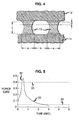
- FIG. 5 is a graph of a curve 32 showing the force F in pounds on the load cell as a function of time; the signal transmitted by the load cell is proportional to such force.
- a first threshold 33 such as, for example, 0.4 pounds
- the computer 30 of FIG. 3 is programmed to stop vertical movement of the pick-up tool and simultaneously to actuate heater 20 of FIG. 1.
- contact element 21 is in contact with chip 12 and the heater heats the chip via contact element 21 so as to melt the solder bonds 13.
- FIG. 4 there is shown an enlargement of part of the integrated circuit chip 12, the substrate 14 and solder bonds 13 of FIG. 1.
- the dimension a of each side of the bonding pads is one hundred microns, and the separation b between successive bonding pads is one hundred microns.
- the height h of each of the solder bonds is approximately ninety microns.
- the integrated circuit chip may be eight millimeters on a side and there may be as many as eighty bonding pads on each side of the chip. With eighty bonding pads on each side of the chip, there may be as many as three hundred solder elements 13 between the integrated circuit chip and the substrate; these solder elements are used for interconnection as well as for structural bonding.
- bridging One can appreciate that if the melting and lift off of the integrated circuit chip are not carefully controlled, one runs a high risk of molten solder unintentionally short circuiting adjacent bonding pads, which is known as "bridging.”
- the invention uses a strain gauge to detect a point at which there is melting to some suitable depth d of the solder bonds 13. Such melting of the solder to a suitable depth results in a decline of curve 32 of FIG. 5 so as to cross the threshold 34. Thus, one is able to actuate the pick-up tool and remove the chip before there has been complete melting of a major portion of the solder bonds 13. This greatly reduces the likelihood of bridging and leaves on the substrate 14 predictable quantities of remnant solder.
- the remnant solder can in turn be removed, for example, by the apparatus described in the U.S. patent of Liu et al., No. 4,923,521 granted May 8, 1990, and hereby incorporated by reference herein.
- the Liu et al. patent describes a method for using a heated solder wick for removing solder remnants from substrate bonding pads by capillary action.
- Certain AVP modules with which I have worked have as many as twenty-four integrated circuit chips on a single substrate. It can be appreciated that the electronics defined on such a module are quite complex and the chances are fairly high that it may be desired to remove a single chip from the completed module.
- the invention can be used to great advantage, particularly where there are a large number of solder bonds separated by an exceedingly small distance and it is imperative to avoid the bridging problem.
- the invention permits the removal without appreciably heating adjacent integrated circuit chips or their solder bonds.
- the operation of the robot for controlling the vacuum pick-up tool is well understood in the art and therefore has not been described in great detail, but, from the foregoing, one skilled in the art may appreciate the ease with which the invention can be applied to known robotic tools.
- the fabrication of a load cell using strain gauges in a resistance bridge connection so as to generate electrical signals in response to an applied mechanical load is also well understood in the art and therefore has not been described in great detail.
- Load cell as used herein is intended to mean any device or aggregate of devices such as piezoelectric devices and strain gauges that generate an electrical signal in response to an applied force.
Landscapes
- Engineering & Computer Science (AREA)
- Manufacturing & Machinery (AREA)
- Microelectronics & Electronic Packaging (AREA)
- Mechanical Engineering (AREA)
- Wire Bonding (AREA)
- Electric Connection Of Electric Components To Printed Circuits (AREA)
- Die Bonding (AREA)
Applications Claiming Priority (2)
| Application Number | Priority Date | Filing Date | Title |
|---|---|---|---|
| US07/584,831 US5065933A (en) | 1990-09-19 | 1990-09-19 | Electronic device manipulating apparatus and method |
| US584831 | 1996-01-11 |
Publications (3)
| Publication Number | Publication Date |
|---|---|
| EP0476912A2 true EP0476912A2 (fr) | 1992-03-25 |
| EP0476912A3 EP0476912A3 (en) | 1992-09-09 |
| EP0476912B1 EP0476912B1 (fr) | 1995-06-21 |
Family
ID=24338960
Family Applications (1)
| Application Number | Title | Priority Date | Filing Date |
|---|---|---|---|
| EP91308269A Expired - Lifetime EP0476912B1 (fr) | 1990-09-19 | 1991-09-11 | Appareil et méthode de manipulation d'un élément électronique |
Country Status (6)
| Country | Link |
|---|---|
| US (1) | US5065933A (fr) |
| EP (1) | EP0476912B1 (fr) |
| JP (1) | JPH0736470B2 (fr) |
| KR (1) | KR920007515A (fr) |
| DE (1) | DE69110596T2 (fr) |
| HK (1) | HK103896A (fr) |
Cited By (5)
| Publication number | Priority date | Publication date | Assignee | Title |
|---|---|---|---|---|
| DE4417625A1 (de) * | 1994-05-19 | 1995-11-30 | Amatech Gmbh & Co Kg | Vorrichtung zur Aufnahme und Führung einer Verbindungseinrichtung |
| EP0736355A3 (fr) * | 1995-04-03 | 1997-07-23 | Heckendorn Larry C | Capteur pour le soudage par résistance |
| EP0714123A3 (fr) * | 1994-11-22 | 1998-06-10 | Sharp Kabushiki Kaisha | Dispositif semi-conducteur, substrat de montage du dispositif semi-conducteur, et procédé de remplacement du dispositif semi-conducteur |
| DE10016998C1 (de) * | 2000-04-05 | 2001-09-13 | Siemens Ag | Bestückvorrichtung mit einer Einrichtung zum Messen der Aufsetzkraft |
| WO2017217931A1 (fr) * | 2016-06-15 | 2017-12-21 | Semiconductor Technologies And Instruments Pte Ltd | Appareil et procédé pour réglage automatique, calibrage et surveillance ou mesure de la position et de la force d'une tête de capteur pendant des opérations de récupération de composants |
Families Citing this family (15)
| Publication number | Priority date | Publication date | Assignee | Title |
|---|---|---|---|---|
| US5174016A (en) * | 1991-04-25 | 1992-12-29 | Toddco General, Inc. | Chip removal apparatus and method of using same |
| US5285946A (en) * | 1991-10-11 | 1994-02-15 | Sanyo Electric Co., Ltd. | Apparatus for mounting components |
| US5523642A (en) * | 1992-09-28 | 1996-06-04 | Sanyo Electric Co., Ltd. | External force measuring system and component mounting apparatus equipped with same |
| US5601675A (en) * | 1994-12-06 | 1997-02-11 | International Business Machines Corporation | Reworkable electronic apparatus having a fusible layer for adhesively attached components, and method therefor |
| US5605277A (en) * | 1994-12-20 | 1997-02-25 | International Business Machines Corporation | Hot vacuum device removal process and apparatus |
| EP0991310B1 (fr) * | 1996-04-16 | 2004-08-04 | Matsushita Electric Industrial Co., Ltd. | Procede et dispositif servant a enlever un composant de circuit integre |
| US5909837A (en) * | 1997-05-09 | 1999-06-08 | Quad Systems Corporation | Contactless bonding tool heater |
| US5920464A (en) * | 1997-09-22 | 1999-07-06 | Trw Inc. | Reworkable microelectronic multi-chip module |
| US6196439B1 (en) * | 1998-05-29 | 2001-03-06 | International Business Machines Corporation | Method and apparatus for μBGA removal and reattach |
| US6216937B1 (en) * | 1999-12-22 | 2001-04-17 | International Business Machines Corporation | Process and apparatus to remove closely spaced chips on a multi-chip module |
| US7296727B2 (en) * | 2001-06-27 | 2007-11-20 | Matsushita Electric Industrial Co., Ltd. | Apparatus and method for mounting electronic components |
| US8113411B2 (en) * | 2010-03-30 | 2012-02-14 | Flextronics Ap, Llc | Universal radio frequency shield removal |
| US8925170B2 (en) | 2011-04-22 | 2015-01-06 | International Business Machines Corporation | Method for removing an electronic component from a substrate |
| US9591795B2 (en) | 2014-09-18 | 2017-03-07 | Lenovo Enterprise Solutions (Singapore) Pte. Ltd. | Sensor-based removal of a soldered device |
| US10269762B2 (en) * | 2015-10-29 | 2019-04-23 | Taiwan Semiconductor Manufacturing Company, Ltd. | Rework process and tool design for semiconductor package |
Family Cites Families (10)
| Publication number | Priority date | Publication date | Assignee | Title |
|---|---|---|---|---|
| US4295596A (en) * | 1979-12-19 | 1981-10-20 | Western Electric Company, Inc. | Methods and apparatus for bonding an article to a metallized substrate |
| EP0117334A3 (fr) * | 1982-11-09 | 1986-01-15 | EMI Limited | Dispositif sensible à plusieurs composantes de force |
| DE8310164U1 (de) * | 1983-04-07 | 1984-01-12 | Cooper Industries, Inc., 77210 Houston, Tex. | Entlötgerät |
| DE3340946A1 (de) * | 1983-11-11 | 1985-05-23 | Siemens AG, 1000 Berlin und 8000 München | Handhabungseinrichtung, insbesondere industrieroboter, mit mindestens einem sensor |
| US4561586A (en) * | 1984-09-04 | 1985-12-31 | Burroughs Corporation | Method of removing a soldered integrated circuit package from a printed circuit board |
| US4611397A (en) * | 1984-10-09 | 1986-09-16 | Universal Instruments Corporation | Pick and place method and apparatus for handling electrical components |
| CA1246121A (fr) * | 1984-11-15 | 1988-12-06 | Westinghouse Electric Corporation | Bras-robot positionneur |
| DE3701652A1 (de) * | 1987-01-21 | 1988-08-04 | Siemens Ag | Ueberwachung von bondparametern waehrend des bondvorganges |
| US4923521A (en) * | 1988-10-11 | 1990-05-08 | American Telephone And Telegraph Company | Method and apparatus for removing solder |
| US4934582A (en) * | 1989-09-20 | 1990-06-19 | Microelectronics And Computer Technology Corporation | Method and apparatus for removing solder mounted electronic components |
-
1990
- 1990-09-19 US US07/584,831 patent/US5065933A/en not_active Expired - Fee Related
-
1991
- 1991-09-03 KR KR1019910015317A patent/KR920007515A/ko not_active Ceased
- 1991-09-04 JP JP3250229A patent/JPH0736470B2/ja not_active Expired - Fee Related
- 1991-09-11 DE DE69110596T patent/DE69110596T2/de not_active Expired - Fee Related
- 1991-09-11 EP EP91308269A patent/EP0476912B1/fr not_active Expired - Lifetime
-
1996
- 1996-06-13 HK HK103896A patent/HK103896A/en not_active IP Right Cessation
Cited By (7)
| Publication number | Priority date | Publication date | Assignee | Title |
|---|---|---|---|---|
| DE4417625A1 (de) * | 1994-05-19 | 1995-11-30 | Amatech Gmbh & Co Kg | Vorrichtung zur Aufnahme und Führung einer Verbindungseinrichtung |
| WO1995032073A1 (fr) * | 1994-05-19 | 1995-11-30 | David Finn | Dispositif de fixation et de guidage d'un element d'assemblage |
| DE4417625C2 (de) * | 1994-05-19 | 1999-05-20 | Amatech Gmbh & Co Kg | Vorrichtung zur Aufnahme und Führung einer Verbindungseinrichtung |
| EP0714123A3 (fr) * | 1994-11-22 | 1998-06-10 | Sharp Kabushiki Kaisha | Dispositif semi-conducteur, substrat de montage du dispositif semi-conducteur, et procédé de remplacement du dispositif semi-conducteur |
| EP0736355A3 (fr) * | 1995-04-03 | 1997-07-23 | Heckendorn Larry C | Capteur pour le soudage par résistance |
| DE10016998C1 (de) * | 2000-04-05 | 2001-09-13 | Siemens Ag | Bestückvorrichtung mit einer Einrichtung zum Messen der Aufsetzkraft |
| WO2017217931A1 (fr) * | 2016-06-15 | 2017-12-21 | Semiconductor Technologies And Instruments Pte Ltd | Appareil et procédé pour réglage automatique, calibrage et surveillance ou mesure de la position et de la force d'une tête de capteur pendant des opérations de récupération de composants |
Also Published As
| Publication number | Publication date |
|---|---|
| JPH04258195A (ja) | 1992-09-14 |
| JPH0736470B2 (ja) | 1995-04-19 |
| EP0476912A3 (en) | 1992-09-09 |
| EP0476912B1 (fr) | 1995-06-21 |
| HK103896A (en) | 1996-06-21 |
| US5065933A (en) | 1991-11-19 |
| DE69110596T2 (de) | 1996-01-11 |
| KR920007515A (ko) | 1992-04-28 |
| DE69110596D1 (de) | 1995-07-27 |
Similar Documents
| Publication | Publication Date | Title |
|---|---|---|
| US5065933A (en) | Electronic device manipulating apparatus and method | |
| US4332341A (en) | Fabrication of circuit packages using solid phase solder bonding | |
| EP0680803A2 (fr) | Assemblage de puces sur un substrat | |
| US5021630A (en) | Laser soldering method and apparatus | |
| US9426898B2 (en) | Thermocompression bonders, methods of operating thermocompression bonders, and interconnect methods for fine pitch flip chip assembly | |
| TWI804584B (zh) | 用於重工倒裝晶片組件的裝置及方法 | |
| US5172469A (en) | Advanced part removal and torque shear station | |
| EP0185326B1 (fr) | Méthode et outil pour le remplacement de fiches individuelles dans un réseau dense de fiches de connexion d'une structure d'emballage pour l'électronique | |
| US6605500B2 (en) | Assembly process | |
| EP0463788B1 (fr) | Procédé pour le montage automatique sur bande | |
| Hatanaka | Packaging processes using flip chip bonder and future directions of technology development | |
| US6712111B2 (en) | Bonding method and apparatus | |
| CN1259705C (zh) | 祼芯片安装方法及安装系统 | |
| Koopman et al. | Flip chip process development techniques using a modified laboratory aligner bonder | |
| JP3095959B2 (ja) | チップ部品の基板への接続方法 | |
| JPH0555744A (ja) | 基板実装部品の着脱装置 | |
| JP2709484B2 (ja) | 半導体装置の製造方法 | |
| JPS6257096B2 (fr) | ||
| JPS61206234A (ja) | 感熱記録ヘツドのicチツプリペア方法 | |
| JP2002134563A (ja) | 半導体製造装置及び半導体製造方法 | |
| JPS6171694A (ja) | 自動検査機能付きワイヤボンダ | |
| JPH07183321A (ja) | ワイヤボンディング装置 | |
| JPH05190552A (ja) | 半導体装置及びその製造方法 | |
| Bock et al. | Electronic Packaging for Ultra Thin and Flexible ICs and Microsystems | |
| Bonding | flexibility, productivity |
Legal Events
| Date | Code | Title | Description |
|---|---|---|---|
| PUAI | Public reference made under article 153(3) epc to a published international application that has entered the european phase |
Free format text: ORIGINAL CODE: 0009012 |
|
| AK | Designated contracting states |
Kind code of ref document: A2 Designated state(s): DE FR GB IT |
|
| PUAL | Search report despatched |
Free format text: ORIGINAL CODE: 0009013 |
|
| AK | Designated contracting states |
Kind code of ref document: A3 Designated state(s): DE FR GB IT |
|
| 17P | Request for examination filed |
Effective date: 19930225 |
|
| 17Q | First examination report despatched |
Effective date: 19931109 |
|
| RAP3 | Party data changed (applicant data changed or rights of an application transferred) |
Owner name: AT&T CORP. |
|
| GRAA | (expected) grant |
Free format text: ORIGINAL CODE: 0009210 |
|
| AK | Designated contracting states |
Kind code of ref document: B1 Designated state(s): DE FR GB IT |
|
| ITF | It: translation for a ep patent filed | ||
| ET | Fr: translation filed | ||
| REF | Corresponds to: |
Ref document number: 69110596 Country of ref document: DE Date of ref document: 19950727 |
|
| PLBE | No opposition filed within time limit |
Free format text: ORIGINAL CODE: 0009261 |
|
| STAA | Information on the status of an ep patent application or granted ep patent |
Free format text: STATUS: NO OPPOSITION FILED WITHIN TIME LIMIT |
|
| 26N | No opposition filed | ||
| PGFP | Annual fee paid to national office [announced via postgrant information from national office to epo] |
Ref country code: FR Payment date: 19990617 Year of fee payment: 9 |
|
| PGFP | Annual fee paid to national office [announced via postgrant information from national office to epo] |
Ref country code: GB Payment date: 19990625 Year of fee payment: 9 |
|
| PGFP | Annual fee paid to national office [announced via postgrant information from national office to epo] |
Ref country code: DE Payment date: 19990930 Year of fee payment: 9 |
|
| PG25 | Lapsed in a contracting state [announced via postgrant information from national office to epo] |
Ref country code: GB Free format text: LAPSE BECAUSE OF NON-PAYMENT OF DUE FEES Effective date: 20000911 |
|
| GBPC | Gb: european patent ceased through non-payment of renewal fee |
Effective date: 20000911 |
|
| PG25 | Lapsed in a contracting state [announced via postgrant information from national office to epo] |
Ref country code: FR Free format text: LAPSE BECAUSE OF NON-PAYMENT OF DUE FEES Effective date: 20010531 |
|
| PG25 | Lapsed in a contracting state [announced via postgrant information from national office to epo] |
Ref country code: DE Free format text: LAPSE BECAUSE OF NON-PAYMENT OF DUE FEES Effective date: 20010601 |
|
| REG | Reference to a national code |
Ref country code: FR Ref legal event code: ST |
|
| PG25 | Lapsed in a contracting state [announced via postgrant information from national office to epo] |
Ref country code: IT Free format text: LAPSE BECAUSE OF NON-PAYMENT OF DUE FEES;WARNING: LAPSES OF ITALIAN PATENTS WITH EFFECTIVE DATE BEFORE 2007 MAY HAVE OCCURRED AT ANY TIME BEFORE 2007. THE CORRECT EFFECTIVE DATE MAY BE DIFFERENT FROM THE ONE RECORDED. Effective date: 20050911 |