EP0477385B1 - Rückstellverfahren für die umsetzerschnittstelle bei störfällen und rechnersystem, welches dieses verfahren anwendet - Google Patents
Rückstellverfahren für die umsetzerschnittstelle bei störfällen und rechnersystem, welches dieses verfahren anwendet Download PDFInfo
- Publication number
- EP0477385B1 EP0477385B1 EP91906978A EP91906978A EP0477385B1 EP 0477385 B1 EP0477385 B1 EP 0477385B1 EP 91906978 A EP91906978 A EP 91906978A EP 91906978 A EP91906978 A EP 91906978A EP 0477385 B1 EP0477385 B1 EP 0477385B1
- Authority
- EP
- European Patent Office
- Prior art keywords
- adaptor
- reset
- module
- firmware
- instruction
- Prior art date
- Legal status (The legal status is an assumption and is not a legal conclusion. Google has not performed a legal analysis and makes no representation as to the accuracy of the status listed.)
- Expired - Lifetime
Links
Images


Classifications
-
- G—PHYSICS
- G06—COMPUTING OR CALCULATING; COUNTING
- G06F—ELECTRIC DIGITAL DATA PROCESSING
- G06F11/00—Error detection; Error correction; Monitoring
- G06F11/07—Responding to the occurrence of a fault, e.g. fault tolerance
- G06F11/14—Error detection or correction of the data by redundancy in operations
- G06F11/1402—Saving, restoring, recovering or retrying
- G06F11/1415—Saving, restoring, recovering or retrying at system level
- G06F11/1438—Restarting or rejuvenating
-
- G—PHYSICS
- G06—COMPUTING OR CALCULATING; COUNTING
- G06F—ELECTRIC DIGITAL DATA PROCESSING
- G06F13/00—Interconnection of, or transfer of information or other signals between, memories, input/output devices or central processing units
- G06F13/10—Program control for peripheral devices
- G06F13/12—Program control for peripheral devices using hardware independent of the central processor, e.g. channel or peripheral processor
- G06F13/124—Program control for peripheral devices using hardware independent of the central processor, e.g. channel or peripheral processor where hardware is a sequential transfer control unit, e.g. microprocessor, peripheral processor or state-machine
- G06F13/126—Program control for peripheral devices using hardware independent of the central processor, e.g. channel or peripheral processor where hardware is a sequential transfer control unit, e.g. microprocessor, peripheral processor or state-machine and has means for transferring I/O instructions and statuses between control unit and main processor
Definitions
- the present invention relates to a reset method when an adaptor module is faulty and a computer system executing the same in a computer system comprising processor modules, adaptor modules, a system bus connecting the two modules, and devices or lines connected to the adaptor modules.
- the module cannot be inserted at the time when the power source is turned ON.
- the reason is as follows. Namely, when one of modules is faulty, logical circuits in each module are constituted so that the necessary data for fault analysis are held. For this reason, each module is held at the various status positions and is not reset automatically.
- the system reset namely, the power source reset is not carried out, a dump instruction, diagnostic instruction, or the like cannot be received.
- the system reset is a system fault and gives users of the computer system difficulty. Therefore, a reset method wherein the users do not experience difficulties even when the adaptor module is in a faulty status, the adaptor module is initialized from the processor module, and the necessary data for the fault analysis can be recorded, becomes necessary.
- An object of the present invention is to provide a reset method when an adaptor module is faulty and a computer system executing the same wherein even when the adaptor module cannot operate, the adaptor module can be initialized efficiently, and the fault information in the adaptor module can be stored and restarted.
- a reset method for a computer system having processor modules, adaptor modules, a system bus connecting the processor modules and the adaptor modules, and a plurality of devices or lines connected to the adaptor modules; each of the adaptor modules having an interface portion for receiving and decoding instructions issued from the processor module and for controlling the connection to the processor module, and an adaptor control portion for controlling data transfer between the system bus and the devices or lines based on the decoded information from the interface portion, the system having a reset instruction issuing means for issuing a reset instruction and each adaptor module further comprising a status designation means for designating the status of the adaptor module; the method being for providing a reset function in the event of an adaptor module being faulty; characterized in that the method comprises a first step in which the processor module issues the reset instruction, having a code, or flag, designating any one of a preselected set of reset operations in the reset instruction, to the adaptor module, each reset operation designating different predetermined portions of the adaptor module to be reset initially
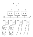
- Figure 1 is a block diagram of the computer system to which the invention is applied
- Fig. 2 shows modules in the system
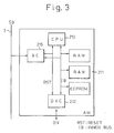
- Fig. 3 shows a constitution of an adaptor control portion of an adaptor module in the module
- Fig. 4 shows an example of an interface portion of the adaptor module.
- a processor module (PM) 1 is connected to the adaptor module (AM) 2 through a system bus (SB) 3, further, various devices (DV) 4 or lines are connected to the adaptor module 2.
- the processor module 1 controls the adaptor module 2 in accordance with instruction from software executed by a central processing unit (CPU) 110 in a control portion 11 shown in Fig. 2, reads data from the device 4, writes data to the device 4, or transmits or receives to or from the line.
- CPU central processing unit
- an instruction for controlling the adaptor module 2 In the instructions issued from the central processing unit 110 of the control portion 11 in the processor module 1 are provided, an instruction for controlling the adaptor module 2, an instruction for controlling the device 4 belonging to the adaptor module 2, and instructions for examining diagnosis or reliability, availability, maintainability or the like.
- Software issues the necessary instruction as a result of a determination of the status of the computer system and the status of the adaptor module 2.
- the processor module 1 and the adaptor module 2, as shown in Fig. 2, for example, are constituted of interface portions 10 and 20 for controlling the interface to the system bus 3, a control portion 11, and an adaptor control portion 21.
- the control portion 11 of the processor module 1 controls the whole system by means of software executed by the central processing unit 110
- the adaptor control portion 21 of the adaptor module 2 controls data transfer between a main storage unit (LSU) 111 of the processor module 1 and the device 4 in accordance with firmware (a microprogram) executed by a control processor (CPU) 210.
- LSU main storage unit
- CPU control processor
- the adaptor module 2 usually has four statuses, namely, an initial status, an operational status, an interruption status, and a non-operational status, which becomes the initial status by a system reset after the power source of the system is turned ON, and becomes the operational status in accordance with the firmware executed by the above-mentioned control processor 210.
- a status register (STR) 200 provided in the interface portion 20 shown in Fig. 4.
- a special instruction issued from the central processing unit 110 of the control portion 11 in the processor module 1 is set in an input register (IRG) 203 of the interface portion 20 of the adaptor module 2, an operating portion of the input register 203 is decoded by a decoder (DEC) 204; when the decoded signal is determined as a reading instruction for the status register 200, the contents of the status register 200 is read to the system bus 3 through a multiplexer (MPX) 202 and an output register (ORG) 201 of the interface portion 20, and are read into the processor module 1.
- MPX multiplexer
- ORG output register
- the interface portion 20 whatever the status of the adaptor module 2 is, can always receive instructions issued by the central processing unit 110 in the processor module 1.
- the adaptor module 2 waits for an instruction from the processor module 1; when the instruction is received by the above input register 203, the decode signal from the decoder 204 is validated, the control processor 210 executes the instruction, for example, data read or write for the device 4 in accordance with the firmware, the execution results are transmitted by the interrupt to the processor module 1 through the interface portion 20, and the adaptor module 2 attains the interruption state by executing the firmware.
- the processor module 1 If the processor module 1 can receive the above result normally, the processor module 1 responds to the adaptor module 2 and a special response instruction is issued. When the adaptor module 2 receives the response instruction at the input register 203, it executes the corresponding firmware, and again attains the operational status. Hereafter, this cycle is repeated and various operations in the system are carried out.
- the adaptor module 2 detects faulty factors in the operation of the system or the adaptor module 2, the adaptor module attains the non-operational status.
- the non-operational status of the adaptor module is set in the status register 200.
- the adaptor module 2 when the adaptor module 2 is faulty and attains the non-operational status, the adaptor module cannot change from the status by its own operation to maintain a faulty status.
- the processor module 1 reads the status of the adaptor module 2, namely, the status of the status register 200, recognizes the non-operational status, issues, for example, a dump instruction or diagnosis instruction to the adaptor module 2, uses a special interface for diagnosis, namely, a scan-in-out-interface, and stores and holds the fault information of the adaptor module 2 in the memory device.
- the above fault information for example, is stored in a special domain in the memory in the adaptor module 2 or is held in a latch in the adaptor module 2.
- the faulty adaptor module 2 is returned to the initial status manually, for example, module reset operation (e.g., push of the reset key provided in the module).
- module reset operation e.g., push of the reset key provided in the module.
- the central processing unit 110 in the processor module 1 executes software, and by instruction from the software, the instruction issued for an instruction control portion (ICNTL) 10a in the processor module (hereinafter abbreviated as PM) 1 is required, then, the instruction control portion 10a requests a right to use the bus to the system bus 3, and when the bus is acquired, the instruction from the control portion of the PM1 is issued to the adaptor module (hereinafter abbreviated as AM) 2 designated by the request.
- INTL instruction control portion
- AM adaptor module
- the firmware When the AM2, as mentioned above, attains an initial status after the power source is turned ON, the firmware starts, and if the status stored in the status register 200 provided in the interface portion 20 (in detail the instruction control portion 20a in Fig. 2) is in an operational state, the firmware monitors the instruction issued before, and the AM2 determines an instruction for itself, and the instruction is read.
- the read instruction decodes the kind of instruction using the decoder (DEC) 204 and is supplied to a control portion CNT1, CNT2 or the like.
- the instruction issued from the PM1 is set in the input register (IRG) 203 regardless of the status of the AM2. But, the output of the decoder 204 is not validated.
- the control portion (CNT1 or CNT2) executes the operation designated by the instruction in accordance with firmware operating under said instruction.
- the instruction control portion 20a of the AM2 interrupts the PM1 to process the process end information, and the instruction control portion 20a attains the interrupt status under control of the firmware.
- the PM1 receives the information normally, then, the normal reception is imparted to the AM2, and the information is received by the input register 203.
- the information is a special response instruction.
- special firmware is executed based on a decoded output of the information, again the operational state is reattained, and a successive process ends.
- Fig. 5 a constitution of the above instruction control portion (ICNTL) 20a in the AM2 is shown.
- the instruction issued from the PM1 is set in the input register 203 provided in the instruction control portion 20a in the AM2 through the system bus 3.
- the decoded result by the decoder 204 is validated, and if the instruction is determined to be for itself, the instruction is sent out to the control portion (CNT1, CNT2 or the like). By providing it with an address of an adaptor, I/O device or the like in the instruction, its destination is determined.
- the control portion comprises, for example, a control portion (CPU 210 in Fig. 2) of the AM2, a control portion (DVC) 212 of the device, and another control portion.
- a control portion CPU 210 in Fig. 2
- DVC control portion
- the instruction control portion 20a includes the status register 200 determining the status of each control portion and displaying the status of the AM2, and the initial status, the operational status, interruption status, and non-operational status defined in the AM2 are set by the execution of the corresponding firmware.
- the conjunction circuit 206 which obtains a logical product of the outputs of the status register 200 and the decoder 204, is provided. Further, even when the AM2 is in a non-operational status, the reset instruction from the PM1 is always monitored.
- RST SIG reset signal
- a function register (FRG) 205 which can copy the contents of the input register (IRG) 203, is provided.
- the AM2 receives the reset instruction for the AM2 from the PM1, and when the reset signal (RST SIG) is output, a portion of or all of the reset instruction is written in the function register 205, all or a portion of the initializing data sent by the preceding instruction of the reset instruction and set in the input register 203 are written in the function register 205.
- the output of the function register 205 is connected to a data bus (DB).
- the AM2 when the AM2 receives the reset instruction for itself, the AM2 performs an initializing operation in accordance with the value set in the function register 205.
- the reset instruction only resets but various operations of the reset are designated. Accordingly, the reset instruction is defined using a plurality of codes or the combination of the reset code and operation codes or flag becomes a reset instruction.
- the reset operation having various statuses can be executed. As a result, a fine control for the initialization can be performed.
- a bus control portion (BC) 215 receives input/output instruction in accordance with the status of the AM2, and the reset instruction can be received in a special state, i.e., during the adaptor module non-operational status.
- the reset instruction issued by the PM1 is the instruction designated to collect dump information of the AM2
- the BC portion 215 of the AM2 decodes the instruction, and as a result, reset signals for resetting portions other than the memory are turned ON and the AM2 is initialized.
- the AM2 attains an operational status after an initial diagnosis, an adaptor dump ready interruption is issued to the PM1 issuing the reset instruction, and the dump instruction is expected. At that time, the AM2 responds to the instruction from the other PM1 as busy and does not receive the instruction so as to receive only the dump instruction from the issued PM1. Then, after receiving the dump instruction, the necessary contents of the memory in the adaptor are transferred to the PM1.
- the usual reset instruction i.e., the reset instruction not designated an operation after reset is issued to the AM2.
- the PM1 issues (77) the reset instruction executing the dump process.
- the AM2 is initialized (78'). Namely, the AM2 is reset (78') except for the memory.
- the reset in this case, is the same as explained in Fig. 6.
- the AM2 attains an operational status (79).
- the AM2 sends a request signal for the interruption of the dump ready to the PM1.
- the interface portion of the BC portion is operational, the readiness of the dump is imparted to the PM.
- the PM1 receives (81) the request and issues (82) the dump instruction to the AM issuing the dump ready interrupt.
- the AM2 receives (83) the dump instruction, it starts to dump (84).
- the contents of the inner memory (RAM) in the AM2 are supplied (85) to the PM1 as fault information.
- the dump is completed (86, 87)
- the reset instruction is issued to the AM from the PM 1.
- the reset instruction at this time is not the reset except for the inner memory at the step (77), and the memory is reset. Accordingly, the AM is completely initialized (90) and attains operational status.
- the function register 205 in the AM2 is shown. If the AM2 receives the reset instruction from PM1, a valid bit (V) in the register is turned ON. At that time, the function code (FUNC) designates whether to patch or not to patch for the firmware. For example, if the function code is "00”, the reset is without patching and if the function code is "01", the reset with patching is defined.
- Step 1 After the AM2 receives the reset instruction (Step 1) and resets the minimum hardware by which the AM2 can operate, the firmware starts to operate.
- the function register 205 in Fig. 8 is examined. If the valid bit is OFF (Step 2), because of no reset due to the instruction, the firmware is at an idle status and waits for the instruction from the PM1. If the valid bit is ON, the function code is examined, if the function code is "00", because of the reset without patching, the firmware attains an idle status as when the valid bit is OFF, and attains a status waiting for the instruction from the PM1.
- Step 2 the firmware reads management information in an EEPROM (Electrically Erasable Programmable Read Only Memory) in Fig. 3 and the information is examined whether it is valid or not (Step 3). If valid data exists, first, the firmware reads the edition number of the current firmware, and recognizes a coincidence with the edition number of the applied firmware (Step 4). If the coincidence is obtained, the data is changed and reads the data designated in the next address similarly. The change of the designated size is completed, and finally, the new edition number is stored.
- EEPROM Electrical Erasable Programmable Read Only Memory
- the firmware in a ROM read only memory included in the control storage (CS) 211 in Fig. 3) is reloaded (Step 6), the edition number in the no patching is stored (Step 7), and the firmware attains an idle status.
- the starting of the firmware executing the patch can be known by the instruction from the PM1.
- the firmware controlling the AM2 is excessively large, the firmware cannot be supplied by the ROM. This is the case of supporting many communication control sequences as in the line system, in the host computer, the sequence of the adaptor support is defined, and after the initial diagnosis only the necessary sequences are down-loaded.
- the ROM of the AM2 the minimum program to down-load the firmware is stored. Usually, after the power source is turned ON, and simultaneously the initial diagnosis is completed, the program in the ROM starts and the firmware is down-loaded from the host computer.
- the down-loaded firmware develops in the RAM (Random Access Memory in Fig. 3) in the AM2; when simultaneously completing the down-loading, the control is transferred to the firmware in the RAM and the operation starts.
- This type of adaptor module designates the down-loading of the firmware in the function code of the reset instruction.
- the PM1 detecting the non-operational status of the AM2 issues the reset instruction (306) by designating the down-loading of the firmware to the parameter when the reset instruction is issued, since in this AM2 it is previously known that it must be down-loaded in the firmware.
- the AM2 receiving (307) the reset instruction turns the signal ON, which resets various portions other than the memory, and the AM2 is initialized (308).
- the AM2 attains operational status (309) after the initial diagnosis, issues (310) a down-loading ready interruption to the PM1 issuing the reset instruction, and waits for the firmware load instruction.
- the PM1 receives (312) the down-loading ready interruption.
- the AM2 waits only for the firmware load instruction from the PM1 issuing the instruction, responds that it is busy to the instruction from the other PM1, and does not receive the instruction.
- the PM1 issues (313) the firmware load instruction.
- the AM receives (314) the firm load instruction and the adaptor down-loads (317) the firmware from the PM1.
- the PM1 completes (317) the down-loading the PM1 issues (319) the reset instruction, which does not designate the operation after reset.
- the above down-loading process steps are shown in Fig. 10.
- the reset signal when the non-operational status is set in the status register (STR) of the interface portion in the AM2, if the reset instruction issued by the PM1 is received, the reset signal outputs to initialize the AM2, and the AM2 can be reset without operators and the software.
- the data information included in the reset instruction is set in the special function register (FRG), and, for example, the AM2 is initialized to execute the dump instruction. Further by providing various contents of the function register (FRG), the reset operation having various states can be carried out.
Landscapes
- Engineering & Computer Science (AREA)
- Theoretical Computer Science (AREA)
- Physics & Mathematics (AREA)
- General Engineering & Computer Science (AREA)
- General Physics & Mathematics (AREA)
- Computer Hardware Design (AREA)
- Microelectronics & Electronic Packaging (AREA)
- Quality & Reliability (AREA)
- Debugging And Monitoring (AREA)
- Retry When Errors Occur (AREA)
Claims (8)
- Rückstellverfahren für ein Computersystem mit Prozessormodulen (1), Adaptermodulen (2), einem Systembus (3), der die Prozessormodule (1) und die Adaptermodule (2) verbindet, und mit einer Vielzahl von Vorrichtungen (4) oder Leitungen, die an die Adaptermodule angeschlossen sind;wobei jeder der Adaptermodule (2) einen Interfaceabschnitt (20) zum Empfangen und zum Decodieren von Befehlen aufweist, die von dem Prozessormodul (1) ausgegeben werden, und um die Verbindung des Prozessormoduls (1) zu steuern, und mit einem Adaptersteuerabschnitt (21) zur Steuerung des Datentransfers zwischen dem Systembus (3) und den Vorrichtungen oder Leitungen auf der Grundlage der decodierten Informationen von dem Interfaceabschnitt, wobei das System eine Rückstellbefehl-Ausgabeeinrichtung enthält, um einen Rückstellbefehl auszugeben, und jeder Adaptermodul ferner eine Statusbezeichnungseinrichtung (205) umfaßt, um den Status des Adaptermoduls zu bezeichnen;wobei das Verfahren dazu dient, eine Rückstellfunktion für den Fall vorzusehen, daß die Statusbezeichnungseinrichtung anzeigt, daß ein Adaptermodul fehlerhaft ist;dadurch gekennzeichnet, daß das Verfahren einen ersten Schritt umfaßt, bei dem der Prozessormodul (1) einen Rückstellbefehl, der einen Code oder ein Flag aufweist, welcher bzw. welches einen vorgewählten Satz von Rückstelloperationen in dem Rückstellbefehl bezeichnet, an den Adaptermodul ausgibt, wobei jede Rückstelloperation vorbestimmte verschiedene Abschnitte des Adaptermoduls bezeichnet, die zu Beginn rückzustellen sind, wodurch alle Abschnitte, ausgenommen der Speicherabschnitt, welche Log-Informationen enthalten, die sich auf den Adaptermodul beziehen, zurückgestellt werden;einen zweiten Schritt bei dem der Adaptermodul (2) den Rückstellbefehl, der von dem Prozessormodul mit dem Code, der den Rückstellbefehl enthält, ausgegeben wurde, nach dem ersten Schritt bei dem Interfaceabschnitt des Busses empfängt;einen dritten Schritt, bei dem der Adaptermodul eine Rückstelloperation ausführt, die durch den Code oder das Flag in dem Rückstellbefehl bezeichnet ist;einen vierten Schritt, bei dem der Prozessormodul den Dumping-Vorgang der Log-Informationen anfragt,einen fünften Schritt, bei dem, nachdem der Adaptermodul die Anfrage empfangen hat, der Adaptermodul die Log-Informationen von dem Speicherabschnitt, der bei dem dritten Schritt nicht zurückgestellt wurde, zu dem Prozessormodul sendet,einen sechsten Schritt, bei dem der Prozessormodul einen weiteren Rückstellbefehl zu dem Adaptermodul sendet, der anzeigt, daß die Arten des Flags oder des Codes der Rückstellbefehle, die durch den ersten Schritt bezeichnet wurden, alle Abschnitte des Adaptermoduls zurückstellen, undeinen siebten Schritt, bei dem, nachdem der Adaptermodul den weiteren Rückstellbefehl empfangen hat, alle Abschnitte des Adaptermoduls zurückgestellt werden.
- Verfahren nach Anspruch 1, bei demder Adaptermodul ein ROM enthält, um Firmware zu speichern, und einen RAM enthält, um die Firmware zu entwikkeln, wobei die Daten des ROM's in dem RAM gespeichert werden und verwendet werden, wobei der Adaptermodul ferner einen Korrekturspeicher umfaßt, der ein Korrekturprogramm speichert, welches ein Korrektur-Update des Firmware-Programms ist, welches in dem ROM gespeichert ist;das Flag oder der Code des ersten Rückstellbefehls bei dem ersten Schritt angibt, ob das Korrekturprogramm auf die Firmware angewendet wird; undbei dem dritten Schritt, nachdem der Adaptermodul zurückgestellt worden ist, wenn das Flag oder der Code die Korrekturoperation bezeichnet, das Ergebnis der Anwendung des Korrekturprogramms auf die Daten, die in dem ROM gespeichert sind, in dem RAM abgelegt bzw. entwickelt wird, und, wenn keine Anwendung der Korrektur bezeichnet wurde, die Inhalte des ROM's unmodifiziert in den RAM geladen werden.
- Verfahren nach Anspruch 1, bei dem der Adaptermodul ein ROM enthält, um Firmware zu speichern, und ferner einen RAM enthält, um die Firmware zu entwickeln,wobei die Daten des ROM's in dem RAM gespeichert werden und verwendet werden;das Flag oder der Code des Rückstellbefehls bei dem ersten Schritt angibt, ob die in dem RAM gespeicherte Firmware zu den Inhalten des ROM's werden soll oder ob dies die Firmware sein soll, die von dem Prozessormodul geliefert wird; undbei dem dritten Schritt, nachdem der Adaptermodul zurückgestellt worden ist, dann, wenn das Flag oder der Code, der angibt, daß die ROM-Daten in dem RAM gespeichert werden, die ROM-Daten in dem RAM entwickelt werden, und dann, wenn das Flag oder der Code, der anzeigt, daß die von dem Prozessormodul übertragene Firmware in den RAM geladen wird, die Daten von dem Prozessormodul übertragen werden und dann die Daten in dem RAM gespeichert werden.
- Verfahren nach Anspruch 1, bei dem bei dem ersten Schritt ein Rückstellbefehl, der ein Flag oder einen Code enthält, welcher die Übertragung der Fehlerinformationen der Adaptermodule bezeichnet, an dem Prozessormodul ausgegeben wird, und
bei dem dritten Schritt die Fehlerinformationen des Adaptermoduls zu dem Prozessormodul übertragen werden und dieser zurückgestellt wird, wenn die Rückstellinformation, die den Code enthält, empfangen wird. - Computersystem mit Prozessormodulen (1), Adaptermodulen (2), einem Systembus (3), welcher die Prozessormodule und die Adaptermodule verbindet, und mit einer Vielzahl von Vorrichtungen (4) oder einer Vielzahl von Leitungen, die an die Adaptermodule angeschlossen sind; wobei jeder der Adaptermodule einen Interfaceabschnitt (20) enthält, um Decodierinstruktionen zu empfangen, die von dem Prozessormodul ausgegeben werden, und um die Verbindung des Prozessormoduls und eines Adaptersteuerabschnitts (21) zu steuern, um den Datentransfer zwischen dem Systembus und den Vorrichtungen oder den Leitungen basierend auf den decodierten Informationen von dem Interfaceabschnitt zu steuern; wobei die Adaptermodule ferner aufweisen:eine Statusbezeichnungseinrichtung (205), die in dem Interfaceabschnitt des Adaptermoduls vorgesehen ist, um den Status des Adaptermoduls zu bezeichnen;eine Rückstellbefehl-Ausgabeeinrichtung zum Ausgeben eines Rückstellbefehls, der aus einem Befehl besteht, um den Adapter zurückzustellen und welcher ein Flag oder einen Code enthält, der einen oder mehrere Abschnitte innerhalb des Adapters bezeichnet, die nicht rückzustellen sind, wenn der Prozessormodul den Nicht-Betriebsstatus detektiert, der durch die Statusbezeichnungseinrichtung des Adaptermoduls bezeichnet ist; undeine Einrichtung zum Decodieren des Rückstellbefehls und zum Ausgeben des Rückstellsignals entsprechend dem Code, und zwar lediglich an solche Abschnitte, die beabsichtigt in dem Adaptermodul rückzustellen sind, wenn der Interfaceabschnitt den Rückstellbefehl empfängt;wobei nach einem ersten Rückstellbefehl dieser alle Abschnitte des Adaptermoduls, ausgenommen den Speicherabschnitt, welcher die Log-Informationen enthält, zurückgestellt, und eine Einrichtung vorgesehen ist, um die Log-Informationen, die in dem Speicherabschnitt gespeichert sind, der nicht rückgestellt wurde, zu dem Prozessormodul zu leiten, wobei diese Informationen aktiviert werden, und wobei ferner eine Einrichtung vorgesehen ist, um einen zweiten Rückstellbefehl an alle Abschnitte des Adaptermoduls auszugeben, nachdem die Log-Informationen an den Prozessormodul übertragen wurden.
- Computersystem nach Anspruch 5, bei dem der Adaptermodul ein ROM zum Speichern von Firmware, einen RAM zum Speichern der Firmware, die in dem ROM gespeichert ist, und eine Korrektur-Firmware-Speichereinrichtung umfaßt, um die korrigierten Informationen zu speichern, wenn welche vorhanden sind, und zwar von den Firmware-Daten, die in dem ROM abgelegt sind;der Adaptermodul die Daten korrigiert, die in dem ROM abgelegt sind, und zwar auf der Grundlage der Korrekturinformationen, die korrigierte Firmware in den RAM einspeichert und die Firmware ausführt;die Rückstellbefehls-Ausgabeeinrichtung den Rückstellbefehl ausgibt, dessen Code anzeigt, ob die in dem RAM gespeicherte Firmware lediglich aus den Daten des ROM's besteht oder aus der korrigierten Firmware besteht;das System eine Einrichtung enthält, um, nachdem das Rückstellsignal ausgegeben wurde, die Firmware-Daten in dem RAM entweder von dem ROM oder von dem Korrektur-Firmware-Speicherbereich des RAM-Speichers in Einklang mit dem Code zu sichern, wenn der Interfaceabschnitt den Rückstellbefehl empfängt.
- Computersystem nach Anspruch 5, bei demder Adaptermodul einen RAM enthält, welcher die Firmware speichert und die Firmware ausführt;die Rückstellbefehl-Ausgabeeinrichtung den Rückstellbefehl an den Adaptermodul ausgibt, welcher Befehl einen Code enthält, der anzeigt, ob die Firmware von dem Prozessormodul oder von einer externen Vorrichtung zugeführt wird;nachdem der Interfaceabschnitt den Rückstellbefehl empfangen hat und das Rückstellsignal ausgibt, dann, wenn der Code, der anzeigt, daß der Rückstellbefehl, der einen Code enthält, welcher anzeigt, ob die Firmware von dem Prozessormodul oder von der externen Vorrichtung zugeführt wird, das Rückstellsignal zu dem Adaptermodul ausgegeben wird, wobei die Statusbezeichnungseinrichtung den Wartestatus für den Firmware-Transfer annimmt;die in dem Prozessormodul oder der externen Vorrichtung vorgesehene Firmware zu dem Adaptermodul zugeführt wird; undder Adaptermodul die gelieferte Firmware in dem RAM korrigiert, wenn der Adaptermodul den entsprechenden Status hat.
- Computersystem nach Anspruch 5, bei dem die Rückstellbefehls-Ausgabeeinrichtung den Rückstellbefehl ausgibt, der einen Code enthält, der angibt, daß die Fehlerinformationen in dem Adapter zu dem Prozessormodul übertragen werden.
Applications Claiming Priority (3)
| Application Number | Priority Date | Filing Date | Title |
|---|---|---|---|
| JP98818/90 | 1990-04-13 | ||
| JP9881890 | 1990-04-13 | ||
| PCT/JP1991/000488 WO1991016678A1 (en) | 1990-04-13 | 1991-04-12 | Method of resetting adapter module at failing time and computer system executing said method |
Publications (3)
| Publication Number | Publication Date |
|---|---|
| EP0477385A1 EP0477385A1 (de) | 1992-04-01 |
| EP0477385A4 EP0477385A4 (en) | 1993-02-24 |
| EP0477385B1 true EP0477385B1 (de) | 1997-12-10 |
Family
ID=14229898
Family Applications (1)
| Application Number | Title | Priority Date | Filing Date |
|---|---|---|---|
| EP91906978A Expired - Lifetime EP0477385B1 (de) | 1990-04-13 | 1991-04-12 | Rückstellverfahren für die umsetzerschnittstelle bei störfällen und rechnersystem, welches dieses verfahren anwendet |
Country Status (6)
| Country | Link |
|---|---|
| US (1) | US5321830A (de) |
| EP (1) | EP0477385B1 (de) |
| AU (1) | AU637227B2 (de) |
| CA (1) | CA2058933C (de) |
| DE (1) | DE69128391T2 (de) |
| WO (1) | WO1991016678A1 (de) |
Families Citing this family (12)
| Publication number | Priority date | Publication date | Assignee | Title |
|---|---|---|---|---|
| US5390324A (en) * | 1992-10-02 | 1995-02-14 | Compaq Computer Corporation | Computer failure recovery and alert system |
| JP2886093B2 (ja) * | 1994-07-28 | 1999-04-26 | 株式会社日立製作所 | 障害処理方法および情報処理システム |
| KR100244836B1 (ko) * | 1995-11-02 | 2000-02-15 | 포만 제프리 엘 | 컴퓨터시스템 및 다수의 기능카드 중 한개의 기능카드를 격리하는 방법 |
| US6049672A (en) * | 1996-03-08 | 2000-04-11 | Texas Instruments Incorporated | Microprocessor with circuits, systems, and methods for operating with patch micro-operation codes and patch microinstruction codes stored in multi-purpose memory structure |
| US6141740A (en) * | 1997-03-03 | 2000-10-31 | Advanced Micro Devices, Inc. | Apparatus and method for microcode patching for generating a next address |
| US5983337A (en) * | 1997-06-12 | 1999-11-09 | Advanced Micro Devices, Inc. | Apparatus and method for patching an instruction by providing a substitute instruction or instructions from an external memory responsive to detecting an opcode of the instruction |
| US6085332A (en) * | 1998-08-07 | 2000-07-04 | Mylex Corporation | Reset design for redundant raid controllers |
| TW406507B (en) * | 1998-10-30 | 2000-09-21 | Kim Man Ki | SECS-I and HSMS converting method |
| US6438664B1 (en) | 1999-10-27 | 2002-08-20 | Advanced Micro Devices, Inc. | Microcode patch device and method for patching microcode using match registers and patch routines |
| JP4443067B2 (ja) * | 2001-04-26 | 2010-03-31 | 富士通マイクロエレクトロニクス株式会社 | プロセッサおよびそのリセット制御方法 |
| US6963942B2 (en) * | 2001-12-04 | 2005-11-08 | Motorola, Inc. | High availability system and method for improved intialization |
| JP2010140361A (ja) * | 2008-12-12 | 2010-06-24 | Fujitsu Microelectronics Ltd | コンピュータシステム及び異常検出回路 |
Family Cites Families (9)
| Publication number | Priority date | Publication date | Assignee | Title |
|---|---|---|---|---|
| JPS5943768B2 (ja) * | 1980-06-13 | 1984-10-24 | 富士通株式会社 | チヤネル装置の初期起動方式 |
| JPS5714926A (en) * | 1980-06-30 | 1982-01-26 | Nec Corp | Reset controlling system of input/output device |
| US4589090A (en) * | 1982-09-21 | 1986-05-13 | Xerox Corporation | Remote processor crash recovery |
| US4901232A (en) * | 1983-05-19 | 1990-02-13 | Data General Corporation | I/O controller for controlling the sequencing of execution of I/O commands and for permitting modification of I/O controller operation by a host processor |
| JPS62209627A (ja) * | 1986-03-10 | 1987-09-14 | Nec Corp | デ−タ処理装置 |
| US4802119A (en) * | 1987-03-17 | 1989-01-31 | Motorola, Inc. | Single chip microcomputer with patching and configuration controlled by on-board non-volatile memory |
| JPH01217614A (ja) * | 1988-02-26 | 1989-08-31 | Fujitsu Ltd | システムリセット制御方式 |
| EP0356538B1 (de) * | 1988-08-27 | 1993-12-22 | International Business Machines Corporation | Einrichtung in einem Datenverarbeitungssystem zur System-Initialisierung und -Rückstellung |
| CA2027799A1 (en) * | 1989-11-03 | 1991-05-04 | David A. Miller | Method and apparatus for independently resetting processors and cache controllers in multiple processor systems |
-
1991
- 1991-04-12 CA CA002058933A patent/CA2058933C/en not_active Expired - Fee Related
- 1991-04-12 DE DE69128391T patent/DE69128391T2/de not_active Expired - Fee Related
- 1991-04-12 AU AU76617/91A patent/AU637227B2/en not_active Ceased
- 1991-04-12 US US07/776,325 patent/US5321830A/en not_active Expired - Fee Related
- 1991-04-12 WO PCT/JP1991/000488 patent/WO1991016678A1/ja not_active Ceased
- 1991-04-12 EP EP91906978A patent/EP0477385B1/de not_active Expired - Lifetime
Also Published As
| Publication number | Publication date |
|---|---|
| EP0477385A1 (de) | 1992-04-01 |
| CA2058933A1 (en) | 1991-10-14 |
| DE69128391D1 (de) | 1998-01-22 |
| DE69128391T2 (de) | 1998-04-02 |
| AU7661791A (en) | 1991-11-11 |
| EP0477385A4 (en) | 1993-02-24 |
| US5321830A (en) | 1994-06-14 |
| AU637227B2 (en) | 1993-05-20 |
| WO1991016678A1 (en) | 1991-10-31 |
| CA2058933C (en) | 1996-10-29 |
Similar Documents
| Publication | Publication Date | Title |
|---|---|---|
| US4852092A (en) | Error recovery system of a multiprocessor system for recovering an error in a processor by making the processor into a checking condition after completion of microprogram restart from a checkpoint | |
| US20110283274A1 (en) | Firmware image update and management | |
| EP0477385B1 (de) | Rückstellverfahren für die umsetzerschnittstelle bei störfällen und rechnersystem, welches dieses verfahren anwendet | |
| JP2760363B2 (ja) | 初期化処理装置 | |
| JP3481737B2 (ja) | ダンプ採取装置およびダンプ採取方法 | |
| US7194614B2 (en) | Boot swap method for multiple processor computer systems | |
| US5987625A (en) | Method and apparatus for testing network bootable devices | |
| US8032791B2 (en) | Diagnosis of and response to failure at reset in a data processing system | |
| US20070157014A1 (en) | Apparatus for remote flashing of a bios memory in a data processing system | |
| EP0372411B1 (de) | Schwebendes Konsolesteuerungssystem | |
| CN119376803A (zh) | 一种远程重启方法、设备、存储介质及计算机程序产品 | |
| JPH09218788A (ja) | インサービス直接ダウンロード方式 | |
| JP3317361B2 (ja) | メモリのバッテリバックアップ制御方式 | |
| JPH08329006A (ja) | 障害通知方式 | |
| JPH0734187B2 (ja) | アダプタモジュール障害時のリセット方法および該方法を行う計算機システム | |
| JP2000347758A (ja) | 情報処理装置 | |
| JPH0973437A (ja) | マルチcpuシステム | |
| JP3470454B2 (ja) | マルチプロセッサシステムの通信制御方法 | |
| JP2909128B2 (ja) | 起動処理の引き継ぎ処理装置 | |
| JPH09198334A (ja) | データ伝送システムの障害管理方法 | |
| JPWO1991016678A1 (ja) | アダプタモジュール障害時のリセット方法および該方法を行う計算機システム | |
| JPH07248929A (ja) | 上位装置及びこれを用いた再立上げシステム | |
| JPS59206941A (ja) | デ−タ処理装置 | |
| JPS6256544B2 (de) | ||
| JPH0721091A (ja) | 電子計算機における停電処理方法 |
Legal Events
| Date | Code | Title | Description |
|---|---|---|---|
| PUAI | Public reference made under article 153(3) epc to a published international application that has entered the european phase |
Free format text: ORIGINAL CODE: 0009012 |
|
| 17P | Request for examination filed |
Effective date: 19920108 |
|
| AK | Designated contracting states |
Kind code of ref document: A1 Designated state(s): DE FR GB |
|
| A4 | Supplementary search report drawn up and despatched |
Effective date: 19930106 |
|
| AK | Designated contracting states |
Kind code of ref document: A4 Designated state(s): DE FR GB |
|
| 17Q | First examination report despatched |
Effective date: 19960227 |
|
| GRAG | Despatch of communication of intention to grant |
Free format text: ORIGINAL CODE: EPIDOS AGRA |
|
| GRAG | Despatch of communication of intention to grant |
Free format text: ORIGINAL CODE: EPIDOS AGRA |
|
| GRAH | Despatch of communication of intention to grant a patent |
Free format text: ORIGINAL CODE: EPIDOS IGRA |
|
| GRAH | Despatch of communication of intention to grant a patent |
Free format text: ORIGINAL CODE: EPIDOS IGRA |
|
| GRAH | Despatch of communication of intention to grant a patent |
Free format text: ORIGINAL CODE: EPIDOS IGRA |
|
| GRAA | (expected) grant |
Free format text: ORIGINAL CODE: 0009210 |
|
| AK | Designated contracting states |
Kind code of ref document: B1 Designated state(s): DE FR GB |
|
| REF | Corresponds to: |
Ref document number: 69128391 Country of ref document: DE Date of ref document: 19980122 |
|
| ET | Fr: translation filed | ||
| PLBE | No opposition filed within time limit |
Free format text: ORIGINAL CODE: 0009261 |
|
| STAA | Information on the status of an ep patent application or granted ep patent |
Free format text: STATUS: NO OPPOSITION FILED WITHIN TIME LIMIT |
|
| 26N | No opposition filed | ||
| REG | Reference to a national code |
Ref country code: GB Ref legal event code: IF02 |
|
| PGFP | Annual fee paid to national office [announced via postgrant information from national office to epo] |
Ref country code: GB Payment date: 20020410 Year of fee payment: 12 Ref country code: FR Payment date: 20020410 Year of fee payment: 12 |
|
| PGFP | Annual fee paid to national office [announced via postgrant information from national office to epo] |
Ref country code: DE Payment date: 20020417 Year of fee payment: 12 |
|
| PG25 | Lapsed in a contracting state [announced via postgrant information from national office to epo] |
Ref country code: GB Free format text: LAPSE BECAUSE OF NON-PAYMENT OF DUE FEES Effective date: 20030412 |
|
| PG25 | Lapsed in a contracting state [announced via postgrant information from national office to epo] |
Ref country code: DE Free format text: LAPSE BECAUSE OF NON-PAYMENT OF DUE FEES Effective date: 20031101 |
|
| GBPC | Gb: european patent ceased through non-payment of renewal fee |
Effective date: 20030412 |
|
| PG25 | Lapsed in a contracting state [announced via postgrant information from national office to epo] |
Ref country code: FR Free format text: LAPSE BECAUSE OF NON-PAYMENT OF DUE FEES Effective date: 20031231 |
|
| REG | Reference to a national code |
Ref country code: FR Ref legal event code: ST |