EP0477941A1 - Tête magnétique de type à effet magnéto-résistif - Google Patents
Tête magnétique de type à effet magnéto-résistif Download PDFInfo
- Publication number
- EP0477941A1 EP0477941A1 EP91116453A EP91116453A EP0477941A1 EP 0477941 A1 EP0477941 A1 EP 0477941A1 EP 91116453 A EP91116453 A EP 91116453A EP 91116453 A EP91116453 A EP 91116453A EP 0477941 A1 EP0477941 A1 EP 0477941A1
- Authority
- EP
- European Patent Office
- Prior art keywords
- thin film
- magnetic
- magneto
- resistance effect
- sensing part
- Prior art date
- Legal status (The legal status is an assumption and is not a legal conclusion. Google has not performed a legal analysis and makes no representation as to the accuracy of the status listed.)
- Granted
Links
Images

Classifications
-
- G—PHYSICS
- G11—INFORMATION STORAGE
- G11B—INFORMATION STORAGE BASED ON RELATIVE MOVEMENT BETWEEN RECORD CARRIER AND TRANSDUCER
- G11B5/00—Recording by magnetisation or demagnetisation of a record carrier; Reproducing by magnetic means; Record carriers therefor
- G11B5/127—Structure or manufacture of heads, e.g. inductive
- G11B5/33—Structure or manufacture of flux-sensitive heads, i.e. for reproduction only; Combination of such heads with means for recording or erasing only
- G11B5/39—Structure or manufacture of flux-sensitive heads, i.e. for reproduction only; Combination of such heads with means for recording or erasing only using magneto-resistive devices or effects
- G11B5/3903—Structure or manufacture of flux-sensitive heads, i.e. for reproduction only; Combination of such heads with means for recording or erasing only using magneto-resistive devices or effects using magnetic thin film layers or their effects, the films being part of integrated structures
-
- G—PHYSICS
- G11—INFORMATION STORAGE
- G11B—INFORMATION STORAGE BASED ON RELATIVE MOVEMENT BETWEEN RECORD CARRIER AND TRANSDUCER
- G11B5/00—Recording by magnetisation or demagnetisation of a record carrier; Reproducing by magnetic means; Record carriers therefor
- G11B5/40—Protective measures on heads, e.g. against excessive temperature
Definitions
- the present invention relates to a magneto-resistance effect type magnetic head.
- MR heads magneto-resistance effect type magnetic heads
- the magnetic head is a floating type
- a slider 52 that floats over a magnetic recording medium 51 (e.g., hard disc) thanks to the air flow created by relative motion of the medium 51 as it rotates.
- the slider 52 contains a conventional composite magnetic head 53 illustratively comprising an inductive type magnetic head for recording and an MR magnetic head for reproduction in an integral manner.
- the slider 52 also has a gimbal 53 composed of an elastic member for supporting the slider 52.
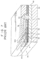
- Fig. 7 is an enlarged partial cutaway perspective view of the composite thin film magnetic head 53.
- This magnetic head 53 is mounted on the above-described slider 52 or on a base 55 such as a substrate attached to the slider.
- the slider 52 or the base 55 comprises a first and a second thin film magnetic core 57 and 58 deposited one upon the other, the cores forming a magnetic gap (g) therebetween at the front ends thereof, the front ends facing the surface opposite to the magnetic recording medium 51, i.e., the air bearing surface (ABS) 56.
- ABS air bearing surface
- the MR sensing part a magneto-resistance effect sensing part 59 comprising at least a magneto-resistance effect thin film (called the MR thin film), the one end or electrode 60a facing the ABS 56.
- Electrodes 60a and 60b are made of conductive thin films.
- a bias conductor 61 that energizes through an insulation layer 62 the MR sensing part 59 so that the latter is magnetized in a predetermined direction. The energizing is performed so that the MR sensing part 59 operates in a characteristic region representing high sensitivity and the linearity of excellent magneto-resistance effect.
- a head coil 63 surrounds a magnetic connection that serves as the contact between the thin film magnetic cores 57 and 58.
- the bias conductor 61 and the head coil 63 are both made of conductive thin films.
- the thin film magnetic head 53 of the above-described construction is called the "composite” head because it comprises a shield type MR magnetic head and an inductive type magnetic head; the shield type MR magnetic head has the MR sensing part 59 between the first and second thin film magnetic cores 57 and 58; and the inductive type magnetic head contains the head coil 63 on the magnetic path formed by the first and second thin film magnetic cores 57 and 58.
- the MR magnetic head has one end of its MR sensing part 59 connected to ground potential Vss.
- a constant current source 64 supplies a sense current (is) across the electrodes 60a and 60b.
- recordings on the magnetic recording medium 51 cause changes in resistance, the changes being detected as voltage changes.
- the surface of the magnetic recording medium 51 develops and accumulates static electricity (i.e., electric charges) due to the air flow mentioned above. If the magnetic head 53 upon starting or stopping, comes sufficiently close to or contacts the surface of the magnetic recording medium 51, a discharge occurs between the ABS 56 of the grounded MR sensing part 59 and the end or the electrode 60a of the MR thin film opposite thereto. A large current triggered by the discharge flows into the MR thin film. That is, the electric charges accumulated on the magnetic recording medium 51 rush into the magnetic head and on to the MR thin film.
- static electricity i.e., electric charges
- the MR thin film is a metal film as small as hundreds of angstroms in thickness to ensure its high sensitivity.
- the discharge current if it flows in, destroys the MR thin film (called static electricity destruction).
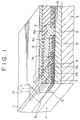
- a magnetoresistance effect type magnetic head comprising (with reference to a partial cutaway perspective view of Fig. 1 and a circuit diagram of Fig. 2): a first and a second thin film magnetic core 1 and 2 deposited one upon the other, the front ends of the magnetic cores 1 and 2 forming a magnetic gap (g) therebetween, the magnetic gap facing the surface (ABS 4 of the slider type magnetic head) opposite to a recording medium (not shown); an MR sensing part 5 having at least one end or one electrode 7a thereof located within the magnetic gap (g), the end or the electrode 7a facing the surface opposite to the magnetic recording medium; and a conductive layer 11 provided close to the second thin film magnetic core 2 and connected to ground, the conductive layer 11 facing the surface opposite to the magnetic recording medium.
- a magneto-resistance effect type magnetic head as defined in the first aspect above, wherein the conductive layer 11 is electrically connected to the second thin film magnetic core 2.
- a magneto-resistance effect type magnetic head as defined in the second aspect above, wherein the conductive layer 11 is electrically connected to one electrode 7a of the MR sensing part 5.
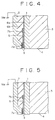
- a magneto-resistance effect type magnetic head comprising (with reference to cross-sectional views of the head in Figs. 4 and 5): a first and a second thin film magnetic core 1 and 2 deposited one upon the other, the front ends of the first and second thin film magnetic cores 1 and 2 forming a magnetic gap therebetween, at least either of the first and second thin film magnetic cores 1 and 2 being conductive; and an MR sensing part 5 having one end or one electrode 7a thereof located within the magnetic gap (g), the end or the electrode 7a being retracted from the front tip of the front ends of the first and second thin film magnetic cores 1 and 2; wherein at least either of the first and second thin film magnetic cores 1 and 2 is connected to ground.
- a floating type magnetic head having the front ends of the first and the second thin film magnetic cores 1 and 2 located flush with the ABS 4 and having the front tip or one electrode 7a of the MR sensing part 5 retracted from the front ends of the cores 1 and 2.
- a floating type magnetic head having the front tip or the electrode 7a of the MR sensing part 5 located flush with the ABS 4, while the first and the second thin film magnetic cores 1 and 2 are allowed to protrude beyond the ABS 4.
- a conductive layer facing the surface opposite to the magnetic recording medium and near the second thin film magnetic core is a conductive layer which is less resistant than the MR sensing part and which is connected to ground. If an electrically charged magnetic recording medium develops a discharge against the magnetic head, the discharge current flows not to the MR sensing part but to the conductive layer. In this manner, possible static electricity destruction (i.e., burning) of the MR sensing part is avoided.
- the conductive layer is electrically connected to the second thin film magnetic core. This arrangement allows the potential between the conductive layer and the second thin film magnetic layer to become substantially the same as the potential across the magnetic gap, whereby electric charges of the magnetic recording medium are prevented from entering the magnetic gap.
- the conductive layer is electrically connected to one electrode of the MR sensing part facing the opposing surface of the magnetic recording medium. This arrangement allows the electric charges rushing from the magnetic recording medium to bypass the MR sensing part and to flow into the conductive layer through the electrode of the MR sensing part.
- the MR sensing part is retracted from the first or second thin film magnetic core 1 or 2 that is connected to ground.
- this arrangement causes the discharge current to bypass the MR sensing part and to flow into the first or second thin film magnetic core that is grounded. In this manner, possible static electricity destruction (burning) of the MR sensing part is avoided.
- any of the magneto-resistance effect type magnetic heads embodying the invention is a composite thin film magnetic head integrally comprising an MR magnetic head for reproduction and an inductive type magnetic head for recording.
- a pair of thin film magnetic cores 1 and 2 are deposited one upon the other with a predetermined clearance in between over E1 base 3 mounted on a slider, the front ends of the cores 1 and 2 forming a magnetic gap (g).
- the core 1 is directly mounted on the base 3.
- the core 1 extends substantially normal to an ABS 4, i.e., the surface opposite to a magnetic recording medium, not shown, in such a way that one end of the core 1 faces the ABS 4.
- the core 2 extends substantially normal to the ABS 4 so that one end of the core 2 faces the ABS 4.
- the front end of the thin film magnetic core 2 facing the ABS 4 is bent towards the thin film magnetic core 1 so that the magnetic gap (g) is formed between the front ends of both cores, the gap facing the ABS 4.
- the thin film magnetic core 2 is in magnetic contact with the core 1 at their back ends, forming a back gap.
- the MR sensing part 5 extends substantially normal to the ABS 4 so that one end of the MR sensing part 5 faces the ABS 4.
- the back end of the MR sensing part 5 reaches an approximate halfway portion of the first and second thin film magnetic cores 1 and 2.
- the MR sensing part 5 is deposited on the thin film magnetic core 1 with a first insulation layer 6a in between over the base 3. This is to ensure insulation between the MR sensing part 5 and the magnetic core 1.
- the MR sensing part 5 comprises a pair of electrodes 7a and 7b through which flows a sense current coming from a constant current source (to be described later), not shown.
- the electrodes 7a and 7b extend substantially normal to the longitudinal direction of the MR sensing part 5 in such a way that the ends of both electrodes are overlaid on both ends of the MR sensing part 5 in the longitudinal direction of the latter.
- the electrode 7a located on the side of the ABS 4, has one crosswise edge thereof facing the ABS 4. The back end of the electrode 7a is bent diagonally backwards relative to the ABS 4.
- a bias conductor 8 On the MR sensing part 5 is a bias conductor 8.
- the bias conductor 8 magnetizes the MR sensing part 5 in a predetermined direction. The magnetizing is done so that the MR sensing part 5 operates in a characteristic region representing high sensitivity and the linearity of excellent magneto-resistance effect.
- the bias conductor 8 is sandwiched between the electrodes 7a and 7b and is substantially in parallel therewith, the tip of the bias conductor 8 being deposited on the MR sensing part 5.
- a spiral-shaped head coil 10 surrounds a magnetic connection 9 that serves as the contact between the first and second thin film magnetic cores 1 and 2.
- the head coil 10 supplies the first and second thin film magnetic cores 1 and 2 with a current corresponding to recorded data.
- the head coil 10 is embedded in a third insulation layer 6c.
- the second thin film magnetic core 2 is overlaid with a grounded conductive layer 11.
- the conductive layer 11 routes to ground the electric charges coming into the magnetic gap from the magnetic recording medium through a fourth insulation layer 6d. Plated with conductive gold (Au) or the like, the conductive layer 11 faces the ABS 4 and is formed all over the base 5. Part of the conductive layer 11 is electrically connected to the second thin film magnetic core 2. This ensures that the potential across the magnetic gap becomes substantially the same as the potential between the conductive layer 11 and the second thin film magnetic core 2. The arrangement prevents electric charges that may come from the magnetic recording medium from rushing into the magnetic gap.
- a core connecting part 12, electrically connecting the conductive layer 11 to the second thin film magnetic core 2 is located at, but not limited by, the approximate center of the core 2; the core connecting part 12 may be located elsewhere as long as its connection to the second thin film magnetic core 2 is secured.
- the conductive layer 11 is connected to the electrode 7a of the MR sensing part 5, the electrode 7a facing the ABS 4.
- This arrangement prevents electric charges that may come from the magnetic recording medium from flowing into the MR sensing part 5. That is, the electrode 7a and the conductive layer 11 are electrically interconnected through a connecting conductive layer 13.
- the connecting conductive layer 13, plated with conductive gold (Au) or the like, is embedded in a rectangular hole. This hole is formed by removing the insulation layers 6b, 6c and 6d from the back end of the electrode 7a. If electric charges rush into the magnetic gap from the magnetic recording medium, the charges bypass the MR sensing part 5 and flow into the electrode 7a connected to the latter. From the electrode 7a, the charges pass through the connecting conductive layer 13 into the conductive layer 11 that is grounded. As a result, the onrush of electric charges into the MR sensing part 5 is prevented and possible static electricity destruction thereof is avoided.
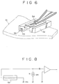
- Fig. 2 is a block diagram of the magneto-resistance effect type magnetic head of the above construction embodying the invention.
- one end of the MR sensing part 5 is connected to around potential Vss.
- a constant current source 14 supplies a sense current (is) across the electrodes 7a and 7b. In this setup, changes in resistance caused by signal fields of the recordings on the magnetic recording medium are detected as changes in voltage.
- the MR sensing part 5 may be alternatively constructed as shown in Fig. 3. That is, a pair of MR thin films 16 and 17 are deposited one upon the other and interconnected on a magnetostatic basis through a non-magnetic insulation layer 15 illustratively made of SiO2. This arrangement prevents the generation of magnetic domain walls and minimizes the Barkhausen noise.
- the above-described first embodiment is manufactured as follows:
- the first thin film magnetic core 1 illustratively made of Fe-Ni is plated onto the base 3 in a predetermined pattern by the known flame plating method, the base 3 being attached to the slider.
- the non-magnetic first insulation layer 6a illustratively made Of SiO2 or Al203 is formed by sputtering or like technique so that the first thin magnetic core 1 is embedded therein.
- the surface of the first insulation layer 6a is flattened. On this surface is formed an MR thin film illustratively made of Ni-Fe, Ni-Co or Ni-Fe-Co, the thin film constituting the MR sensing part 5.
- the MR sensing part 5 extends normal to the ABS 4 so that one end of the MR sensing part 5 faces the ABS 4.
- a conductive layer is formed in a predetermined pattern at both end's of the MR sensing part 5 in the longitudinal direction of the latter.
- the pattern of the conductive layer comprises terminals or wires substantially normal to the MR sensing part 5 and constitutes the electrodes 7a and 7b.
- the electrodes 7a and 7b Covering the electrodes 7a and 7b are the first and second insulation layers 6a and 6b, the layer 6a being formed on the first thin film magnetic core 1, the layer 6b being illustratively made of SiO2 Or Al203.
- the bias conductor 8 is provided across the approximate center of the MR sensing part 5.
- the head coil 10 is formed in spiral shape, the coil 10 being made of a thin film conductive layer and surrounding the magnetic connection 9.
- the third insulation layer 6c is formed over the bias conductor 8 and the head coil 10.
- the first, second and third insulation layers 6a, 6b and 6c are removed to create a window area. Through this area, the first and second thin film magnetic cores 1 and 2 are magnetically interconnected.
- a magnetic thin film illustratively made of Ni-Fe is deposited by sputtering onto the third insulation layer 6c containing the window area, whereby the second thin film magnetic core 2 is created.
- the first and second thin film magnetic cores 1 and 2 are coupled to each other through the window area.
- first and second thin film cores 1 and 2 may be magnetically interconnected by embedding a magnetic layer of a suitable thickness in the window area.
- the fourth insulation layer 6d is formed over the second thin film magnetic core 2.
- the surface of the layer 6d is flattened.
- the second, third and fourth insulation layers 6b, 6c and 6d are removed in a rectangular shape from atop the electrode 7a.
- the hole thus created is filled with Cu plating, constituting the connecting conductive layer 13 that is electrically connected to the conductive layer 11 to be formed later.
- the connecting conductive layer 13 is 20 to 40 ⁇ m in height.
- the conductive layer 11 is then formed by gold-plating the fourth insulation layer 6d. when created in this way, the conductive layer 11 is connected to the connecting conductive layer 13 as well as to part of the second thin film magnetic core 2.
- the electrode 7a of the MR sensing part 5 is connected to ground potential Vss.
- the second embodiment has substantially the same construction as the first embodiment of Fig. 1.
- the second embodiment has the second thin film magnetic core 2 connected to ground.
- the front end of the MR sensing part 5 or of the electrode 7a is retracted backwards from those front ends of the first and second thin film magnetic cores 1 and 2 which face the ABS 4. This arrangement causes electric charges from the magnetic recording medium to flow into the grounded second thin film magnetic core 2 and to bypass the MR sensing part 5. In this manner, possible static electricity destruction of the MR sensing part 5 is avoided.
- Fig. 4 shows one variation of the second embodiment in which the front ends of the first and second thin film magnetic cores 1 and 2 are made flush with the ABS 4 and in which the front end of the MR sensing part 5 or of the electrode 7a is retracted from the front ends of the first and second thin film magnetic cores 1 and 2.
- Fig. 5 depicts another variation of the second embodiment in which the front end of the MR sensing part 5 and that of the electrode 7a are made flush with the ABS 4 and in which the front ends of the first and second thin film magnetic cores 1 and 2 are allowed to protrude beyond the ABS 4.
- like reference characters designate like or corresponding parts, and any repetitive description thereof is omitted.
- the conductive layer which faces the surface opposite to the magnetic recording medium and which is connected to ground is located near the MR sensing part. This arrangement prevents a discharge current that may develop between a charged magnetic recording medium and the magnetic head from flowing into the MR sensing part. Instead, the discharge current flows into the grounded conductive layer. In this manner, possible burning of the MR, sensing part is avoided.
- the conductive layer and the second thin film magnetic core are electrically interconnected. This arrangement makes the potential across the magnetic gap substantially the same as that between the conductive layer and the second thin film magnetic core, thereby suppressing the onrush of electric charges from the magnetic recording medium into the magnetic gap.
- the conductive layer and that electrode of the MR sensing part which faces the ABS are electrically interconnected. This arrangement keeps electric charges that may come from the magnetic recording medium from flowing into the MR sensing part. Instead, the charges flow to the grounded conductive layer through that electrode of the MR sensing part.
- the front end of the MR sensing part or that of one electrode thereof is retracted from the front ends of the first and second thin film magnetic cores.
- This arrangement causes any discharge current that may develop to flow into the first or second thin film magnetic core that is connected to ground, thereby effectively protecting the MR sensing part from possible burning.
Landscapes
- Engineering & Computer Science (AREA)
- Manufacturing & Machinery (AREA)
- Magnetic Heads (AREA)
Applications Claiming Priority (4)
| Application Number | Priority Date | Filing Date | Title |
|---|---|---|---|
| JP25956290 | 1990-09-28 | ||
| JP259562/90 | 1990-09-28 | ||
| JP25567/91 | 1991-01-25 | ||
| JP2556791A JPH04212710A (ja) | 1990-09-28 | 1991-01-25 | 磁気抵抗効果磁気ヘッド |
Publications (2)
| Publication Number | Publication Date |
|---|---|
| EP0477941A1 true EP0477941A1 (fr) | 1992-04-01 |
| EP0477941B1 EP0477941B1 (fr) | 1996-03-06 |
Family
ID=26363202
Family Applications (1)
| Application Number | Title | Priority Date | Filing Date |
|---|---|---|---|
| EP91116453A Expired - Lifetime EP0477941B1 (fr) | 1990-09-28 | 1991-09-26 | Tête magnétique de type à effet magnéto-résistif |
Country Status (3)
| Country | Link |
|---|---|
| US (1) | US5272582A (fr) |
| EP (1) | EP0477941B1 (fr) |
| DE (1) | DE69117634T2 (fr) |
Cited By (3)
| Publication number | Priority date | Publication date | Assignee | Title |
|---|---|---|---|---|
| EP0665534A1 (fr) * | 1994-01-27 | 1995-08-02 | Koninklijke Philips Electronics N.V. | Procédé de fabrication d'une unité de tête magnétique, procédé de fabrication d'une tête magnétique, unité de tête magnétique et tête magnétique pour utilisation dans l'unité |
| EP0621584A3 (fr) * | 1993-04-23 | 1996-07-31 | Sony Corp | Tête magnétique à effet de reluctance magnétique. |
| EP0822540A3 (fr) * | 1993-03-15 | 1998-02-11 | International Business Machines Corporation | Procédé pour fabriquer une unité de support pour transducteur sur un appareil de mémorisation magnétique |
Families Citing this family (38)
| Publication number | Priority date | Publication date | Assignee | Title |
|---|---|---|---|---|
| JP2688173B2 (ja) * | 1993-05-18 | 1997-12-08 | インターナショナル・ビジネス・マシーンズ・コーポレイション | 磁気抵抗読取りトランスジューサ |
| JP2741837B2 (ja) * | 1993-08-06 | 1998-04-22 | インターナショナル・ビジネス・マシーンズ・コーポレイション | 薄膜磁気抵抗ヘッド |
| US5375022A (en) * | 1993-08-06 | 1994-12-20 | International Business Machines Corporation | Magnetic disk drive with electrical shorting protection |
| JPH07192227A (ja) * | 1993-12-28 | 1995-07-28 | Sony Corp | 磁気抵抗効果型磁気ヘッド |
| US5446613A (en) * | 1994-02-28 | 1995-08-29 | Read-Rite Corporation | Magnetic head assembly with MR sensor |
| US5581427A (en) * | 1994-05-04 | 1996-12-03 | International Business Machines Corporation | Peak enhanced magnetoresistive read transducer |
| US6301087B1 (en) * | 1994-07-14 | 2001-10-09 | Nomai S.A. | Magneto-resistive removable hard disk cartridge and disk drive and quadrature embedded servo bursts |
| US5557491A (en) * | 1994-08-18 | 1996-09-17 | International Business Machines Corporation | Two terminal single stripe orthogonal MR head having biasing conductor integral with the lead layers |
| US5587857A (en) * | 1994-10-18 | 1996-12-24 | International Business Machines Corporation | Silicon chip with an integrated magnetoresistive head mounted on a slider |
| US5539598A (en) * | 1994-12-08 | 1996-07-23 | International Business Machines Corporation | Electrostatic protection for a shielded MR sensor |
| US5493467A (en) * | 1994-12-27 | 1996-02-20 | International Business Machines Corporation | Yoke spin valve MR read head |
| US5568335A (en) * | 1994-12-29 | 1996-10-22 | International Business Machines Corporation | Multi-layer gap structure for high resolution magnetoresistive read head |
| US5867350A (en) * | 1995-03-29 | 1999-02-02 | Sony Corporation | Magneto-resistance effect head with insulated bias conductor embedded in shield groove |
| US5761009A (en) | 1995-06-07 | 1998-06-02 | International Business Machines Corporation | Having parastic shield for electrostatic discharge protection |
| US5617273A (en) * | 1995-06-07 | 1997-04-01 | International Business Machines Corporation | Thin film slider with protruding R/W element formed by chemical-mechanical polishing |
| US5638237A (en) * | 1995-08-25 | 1997-06-10 | International Business Machines Corporation | Fusible-link removable shorting of magnetoresistive heads for electrostatic discharge protection |
| US5644454A (en) * | 1996-03-11 | 1997-07-01 | International Business Machines Corporation | Electrostatic discharge protection system for MR heads |
| US5699212A (en) * | 1996-05-01 | 1997-12-16 | International Business Machines Corporation | Method of electrostatic discharge protection of magnetic heads in a magnetic storage system |
| EP0922280A4 (fr) * | 1996-08-30 | 1999-10-13 | Christian P Marlowe | Procede et appareil d'enregistrement magnetique utilisant une decharge induite de plasma |
| JP3151155B2 (ja) * | 1996-09-10 | 2001-04-03 | アルプス電気株式会社 | 薄膜磁気ヘッド |
| KR100238128B1 (ko) * | 1997-04-21 | 2000-01-15 | 윤종용 | 과전류 및 과전압 인가로부터 보호되는 구조의 플래너실리콘헤드 및 그 제조방법 |
| US5986978A (en) * | 1998-01-12 | 1999-11-16 | Read-Rite Corporation | Read/write head and method for magnetic reading and magneto-optical writing on a data storage medium |
| JP2000057524A (ja) * | 1998-08-10 | 2000-02-25 | Fujitsu Ltd | 磁気ヘッドの製造方法 |
| US6583971B1 (en) * | 1999-03-09 | 2003-06-24 | Sae Magnetics (Hk) Ltd. | Elimination of electric-pop noise in MR/GMR device |
| US6324036B1 (en) | 1999-05-26 | 2001-11-27 | International Business Machines Corporation | Combination inductive write head and magnetoresistive (MR) read head with improved topography |
| US6284107B1 (en) | 1999-11-03 | 2001-09-04 | Headway Technologies, Inc. | Method for controlling arcing across thin dielectric film |
| US6415500B1 (en) * | 2000-01-13 | 2002-07-09 | Headway Technologies, Inc. | Method to prevent electrostatic discharge for MR/GMR wafer fabrication |
| US6373660B1 (en) | 2000-03-14 | 2002-04-16 | Read-Rite Corporation | Method and system for providing a permanent shunt for a head gimbal assembly |
| US6470566B2 (en) * | 2001-01-03 | 2002-10-29 | International Business Machines Corporation | ESD protection during GMR head fabrication |
| US6760199B2 (en) | 2001-07-23 | 2004-07-06 | International Business Machines Corporation | Read/write head assembly employing independent read/write shield-pairing and charge-clamped magnetoresistive sensors |
| JP3835237B2 (ja) * | 2001-10-09 | 2006-10-18 | ソニー株式会社 | ヘッドドラム装置および磁気記録再生装置 |
| US6650511B2 (en) | 2002-02-11 | 2003-11-18 | International Business Machines Corporation | Magnetic head assembly with electrostatic discharge (ESD) shunt/pads seed layer |
| US7301732B2 (en) | 2002-08-07 | 2007-11-27 | Headway Technologies, Inc. | GMR head design that suppresses tribocharge during its assembly |
| US6870706B1 (en) * | 2002-08-07 | 2005-03-22 | Headway Technologies, Inc. | Method for suppressing tribocharge in the assembly of magnetic heads |
| US7239488B2 (en) * | 2004-03-09 | 2007-07-03 | Sae Magnetics (H.K.), Ltd. | MR sensor on an insulating substrate and method of manufacture |
| JP2006127609A (ja) * | 2004-10-27 | 2006-05-18 | Hitachi Global Storage Technologies Netherlands Bv | 磁気スライダ及びその製造方法 |
| US7400474B2 (en) * | 2005-10-28 | 2008-07-15 | International Business Machines Corporation | Conductive pairing for piggyback magnetic head |
| US7773349B2 (en) * | 2006-02-10 | 2010-08-10 | Hitachi Global Storage Technologies Netherlands B.V. | Tunnel MR head with long stripe height sensor stabilized through the shield |
Citations (3)
| Publication number | Priority date | Publication date | Assignee | Title |
|---|---|---|---|---|
| EP0152000A2 (fr) * | 1984-01-27 | 1985-08-21 | Hitachi, Ltd. | Transducteur magnétique utilisant l'effet de magnétorésistance |
| EP0221540A2 (fr) * | 1985-11-05 | 1987-05-13 | Sony Corporation | Tête de transducteur magnétique utilisant l'effet de magnétorésistance |
| EP0325365A2 (fr) * | 1988-01-19 | 1989-07-26 | Hewlett-Packard Company | Tête de lecture magnéto-résistive compensée |
Family Cites Families (5)
| Publication number | Priority date | Publication date | Assignee | Title |
|---|---|---|---|---|
| US4499515A (en) * | 1982-07-14 | 1985-02-12 | Minnesota Mining And Manufacturing Company | Integrated magnetostrictive-piezoresistive magnetic recording playback head |
| JPS62245511A (ja) * | 1986-04-18 | 1987-10-26 | Hitachi Ltd | 磁気抵抗効果形磁気ヘツド及びその製造方法 |
| JPS63202979A (ja) * | 1987-02-18 | 1988-08-22 | Alps Electric Co Ltd | エンコ−ダ用磁気センサ |
| US4860138A (en) * | 1987-11-12 | 1989-08-22 | International Business Machines Corp. | Differentially sensitive single track read/write head design with improved biasing |
| US4816947A (en) * | 1987-11-12 | 1989-03-28 | International Business Machines | Single track vertical and horizontal recording read/write head design |
-
1991
- 1991-09-26 EP EP91116453A patent/EP0477941B1/fr not_active Expired - Lifetime
- 1991-09-26 DE DE69117634T patent/DE69117634T2/de not_active Expired - Fee Related
- 1991-09-27 US US07/766,503 patent/US5272582A/en not_active Expired - Fee Related
Patent Citations (3)
| Publication number | Priority date | Publication date | Assignee | Title |
|---|---|---|---|---|
| EP0152000A2 (fr) * | 1984-01-27 | 1985-08-21 | Hitachi, Ltd. | Transducteur magnétique utilisant l'effet de magnétorésistance |
| EP0221540A2 (fr) * | 1985-11-05 | 1987-05-13 | Sony Corporation | Tête de transducteur magnétique utilisant l'effet de magnétorésistance |
| EP0325365A2 (fr) * | 1988-01-19 | 1989-07-26 | Hewlett-Packard Company | Tête de lecture magnéto-résistive compensée |
Cited By (5)
| Publication number | Priority date | Publication date | Assignee | Title |
|---|---|---|---|---|
| EP0822540A3 (fr) * | 1993-03-15 | 1998-02-11 | International Business Machines Corporation | Procédé pour fabriquer une unité de support pour transducteur sur un appareil de mémorisation magnétique |
| EP0621584A3 (fr) * | 1993-04-23 | 1996-07-31 | Sony Corp | Tête magnétique à effet de reluctance magnétique. |
| US6130810A (en) * | 1993-04-23 | 2000-10-10 | Sony Corporation | Magnetic reluctance effect magnetic head with the connection length of the forward electrode less than the facing length of the magnetic gap |
| EP0665534A1 (fr) * | 1994-01-27 | 1995-08-02 | Koninklijke Philips Electronics N.V. | Procédé de fabrication d'une unité de tête magnétique, procédé de fabrication d'une tête magnétique, unité de tête magnétique et tête magnétique pour utilisation dans l'unité |
| BE1008051A3 (nl) * | 1994-01-27 | 1996-01-03 | Koninkl Philips Electronics Nv | Werkwijze voor het vervaardigen van een magneetkopeenheid, werkwijze voor het vervaardigen van een magneetkop, magneetkopeenheid en magneetkop ten gebruike in de magneetkopeenheid. |
Also Published As
| Publication number | Publication date |
|---|---|
| EP0477941B1 (fr) | 1996-03-06 |
| DE69117634D1 (de) | 1996-04-11 |
| US5272582A (en) | 1993-12-21 |
| DE69117634T2 (de) | 1996-10-24 |
Similar Documents
| Publication | Publication Date | Title |
|---|---|---|
| US5272582A (en) | Magneto-resistance effect magnetic head with static electricity protection | |
| US5805390A (en) | Method of fabricating magnetoresistive effect type magnetic head capable of preventing electrostatic damage | |
| US5438470A (en) | Magnetoresistive structure with contiguous junction hard bias design with low lead resistance | |
| US6078479A (en) | Magnetic tape head with flux sensing element | |
| US6163443A (en) | Actuator having MR element protecting means | |
| US6160688A (en) | Magneto-resistive composite head and a magnetic disk device, having grounded magnetic shielding layers | |
| US5907459A (en) | Magnetoresistive thin film magnetic head with specific shapes of leads | |
| EP0459404B1 (fr) | Tête à film mince à effet magnétorésistif | |
| US5978181A (en) | Magnetic head and magnetic recording/reproducing apparatus | |
| CA1182905A (fr) | Tete de transducteur magnetique utilisant la magnetoresistance | |
| EP0475397A2 (fr) | Tête magnétique planaire à film mince | |
| EP0021392A1 (fr) | Structures de tête transductrice magnétique | |
| US7199982B2 (en) | Eliminating ESD exposure for read/write head with heating element | |
| EP0204902B1 (fr) | Tête de transducteur magnétique du type à culasse utilisant un effet magnétorésistif | |
| US6331924B1 (en) | Magnetoresistive head using a magnetoresistive element as a magnetic detector | |
| EP0457278B1 (fr) | Tête magnétique à film mince à effet de magnétorésistance | |
| US6671137B2 (en) | Magnetoresistive head including earth members | |
| EP0482642B1 (fr) | Tête magnétique composite magnétorésistive à film mince | |
| JPS6196508A (ja) | 薄膜磁気ヘツドの構造 | |
| JPH04137212A (ja) | 磁気抵抗効果磁気ヘッド | |
| JPH0540920A (ja) | 複合型磁気ヘツド及びその製造方法 | |
| JPH04212710A (ja) | 磁気抵抗効果磁気ヘッド | |
| EP0549031A1 (fr) | Tête magnétique à couche mince ayant un polymère sur des sections interrompues de guide de flux, méthode de production et structure integrée l'incorporant | |
| JPH06168413A (ja) | 複合型磁気ヘッド | |
| JPH06162447A (ja) | 薄膜磁気ヘッド |
Legal Events
| Date | Code | Title | Description |
|---|---|---|---|
| PUAI | Public reference made under article 153(3) epc to a published international application that has entered the european phase |
Free format text: ORIGINAL CODE: 0009012 |
|
| AK | Designated contracting states |
Kind code of ref document: A1 Designated state(s): DE FR GB |
|
| 17P | Request for examination filed |
Effective date: 19920828 |
|
| 17Q | First examination report despatched |
Effective date: 19941128 |
|
| GRAH | Despatch of communication of intention to grant a patent |
Free format text: ORIGINAL CODE: EPIDOS IGRA |
|
| GRAA | (expected) grant |
Free format text: ORIGINAL CODE: 0009210 |
|
| AK | Designated contracting states |
Kind code of ref document: B1 Designated state(s): DE FR GB |
|
| REF | Corresponds to: |
Ref document number: 69117634 Country of ref document: DE Date of ref document: 19960411 |
|
| ET | Fr: translation filed | ||
| PLBE | No opposition filed within time limit |
Free format text: ORIGINAL CODE: 0009261 |
|
| STAA | Information on the status of an ep patent application or granted ep patent |
Free format text: STATUS: NO OPPOSITION FILED WITHIN TIME LIMIT |
|
| 26N | No opposition filed | ||
| PGFP | Annual fee paid to national office [announced via postgrant information from national office to epo] |
Ref country code: FR Payment date: 20010911 Year of fee payment: 11 |
|
| PGFP | Annual fee paid to national office [announced via postgrant information from national office to epo] |
Ref country code: GB Payment date: 20010926 Year of fee payment: 11 |
|
| PGFP | Annual fee paid to national office [announced via postgrant information from national office to epo] |
Ref country code: DE Payment date: 20011009 Year of fee payment: 11 |
|
| REG | Reference to a national code |
Ref country code: GB Ref legal event code: IF02 |
|
| PG25 | Lapsed in a contracting state [announced via postgrant information from national office to epo] |
Ref country code: GB Free format text: LAPSE BECAUSE OF NON-PAYMENT OF DUE FEES Effective date: 20020926 |
|
| PG25 | Lapsed in a contracting state [announced via postgrant information from national office to epo] |
Ref country code: DE Free format text: LAPSE BECAUSE OF NON-PAYMENT OF DUE FEES Effective date: 20030401 |
|
| GBPC | Gb: european patent ceased through non-payment of renewal fee |
Effective date: 20020926 |
|
| PG25 | Lapsed in a contracting state [announced via postgrant information from national office to epo] |
Ref country code: FR Free format text: LAPSE BECAUSE OF NON-PAYMENT OF DUE FEES Effective date: 20030603 |
|
| REG | Reference to a national code |
Ref country code: FR Ref legal event code: ST |