EP0478004A2 - Transistor mit isolierter Steuerelektrode mit niedriger Drain-Source Betriebsspannung - Google Patents
Transistor mit isolierter Steuerelektrode mit niedriger Drain-Source Betriebsspannung Download PDFInfo
- Publication number
- EP0478004A2 EP0478004A2 EP91119868A EP91119868A EP0478004A2 EP 0478004 A2 EP0478004 A2 EP 0478004A2 EP 91119868 A EP91119868 A EP 91119868A EP 91119868 A EP91119868 A EP 91119868A EP 0478004 A2 EP0478004 A2 EP 0478004A2
- Authority
- EP
- European Patent Office
- Prior art keywords
- region
- semiconductor
- conductivity type
- drain
- surface portion
- Prior art date
- Legal status (The legal status is an assumption and is not a legal conclusion. Google has not performed a legal analysis and makes no representation as to the accuracy of the status listed.)
- Withdrawn
Links
- 239000004065 semiconductor Substances 0.000 claims abstract description 46
- 239000012212 insulator Substances 0.000 claims abstract description 13
- 239000012535 impurity Substances 0.000 claims description 31
- 239000000758 substrate Substances 0.000 description 21
- 230000005669 field effect Effects 0.000 description 12
- VYPSYNLAJGMNEJ-UHFFFAOYSA-N Silicium dioxide Chemical compound O=[Si]=O VYPSYNLAJGMNEJ-UHFFFAOYSA-N 0.000 description 10
- 239000008186 active pharmaceutical agent Substances 0.000 description 8
- 229910052782 aluminium Inorganic materials 0.000 description 8
- XAGFODPZIPBFFR-UHFFFAOYSA-N aluminium Chemical compound [Al] XAGFODPZIPBFFR-UHFFFAOYSA-N 0.000 description 8
- 238000002347 injection Methods 0.000 description 5
- 239000007924 injection Substances 0.000 description 5
- 230000009471 action Effects 0.000 description 4
- 239000000969 carrier Substances 0.000 description 4
- 229910052681 coesite Inorganic materials 0.000 description 4
- 229910052906 cristobalite Inorganic materials 0.000 description 4
- 239000000377 silicon dioxide Substances 0.000 description 4
- 235000012239 silicon dioxide Nutrition 0.000 description 4
- 229910052682 stishovite Inorganic materials 0.000 description 4
- 229910052905 tridymite Inorganic materials 0.000 description 4
- 238000007599 discharging Methods 0.000 description 3
- 230000006872 improvement Effects 0.000 description 3
- 229910021420 polycrystalline silicon Inorganic materials 0.000 description 3
- 229910021421 monocrystalline silicon Inorganic materials 0.000 description 2
- 230000006798 recombination Effects 0.000 description 2
- 238000005215 recombination Methods 0.000 description 2
- 229910052814 silicon oxide Inorganic materials 0.000 description 2
- 229910018487 Ni—Cr Inorganic materials 0.000 description 1
- 230000001419 dependent effect Effects 0.000 description 1
- 238000011161 development Methods 0.000 description 1
- 230000018109 developmental process Effects 0.000 description 1
- 238000009792 diffusion process Methods 0.000 description 1
- 230000000694 effects Effects 0.000 description 1
- 238000002955 isolation Methods 0.000 description 1
- 239000000463 material Substances 0.000 description 1
- 229910052751 metal Inorganic materials 0.000 description 1
- 239000002184 metal Substances 0.000 description 1
- 230000004048 modification Effects 0.000 description 1
- 238000012986 modification Methods 0.000 description 1
- 230000004044 response Effects 0.000 description 1
Images


Classifications
-
- H—ELECTRICITY
- H10—SEMICONDUCTOR DEVICES; ELECTRIC SOLID-STATE DEVICES NOT OTHERWISE PROVIDED FOR
- H10D—INORGANIC ELECTRIC SEMICONDUCTOR DEVICES
- H10D62/00—Semiconductor bodies, or regions thereof, of devices having potential barriers
- H10D62/10—Shapes, relative sizes or dispositions of the regions of the semiconductor bodies; Shapes of the semiconductor bodies
- H10D62/13—Semiconductor regions connected to electrodes carrying current to be rectified, amplified or switched, e.g. source or drain regions
- H10D62/141—Anode or cathode regions of thyristors; Collector or emitter regions of gated bipolar-mode devices, e.g. of IGBTs
- H10D62/142—Anode regions of thyristors or collector regions of gated bipolar-mode devices
-
- H—ELECTRICITY
- H10—SEMICONDUCTOR DEVICES; ELECTRIC SOLID-STATE DEVICES NOT OTHERWISE PROVIDED FOR
- H10D—INORGANIC ELECTRIC SEMICONDUCTOR DEVICES
- H10D1/00—Resistors, capacitors or inductors
- H10D1/40—Resistors
- H10D1/43—Resistors having PN junctions
-
- H—ELECTRICITY
- H10—SEMICONDUCTOR DEVICES; ELECTRIC SOLID-STATE DEVICES NOT OTHERWISE PROVIDED FOR
- H10D—INORGANIC ELECTRIC SEMICONDUCTOR DEVICES
- H10D12/00—Bipolar devices controlled by the field effect, e.g. insulated-gate bipolar transistors [IGBT]
- H10D12/411—Insulated-gate bipolar transistors [IGBT]
- H10D12/441—Vertical IGBTs
- H10D12/491—Vertical IGBTs having both emitter contacts and collector contacts in the same substrate side
-
- H—ELECTRICITY
- H10—SEMICONDUCTOR DEVICES; ELECTRIC SOLID-STATE DEVICES NOT OTHERWISE PROVIDED FOR
- H10D—INORGANIC ELECTRIC SEMICONDUCTOR DEVICES
- H10D64/00—Electrodes of devices having potential barriers
- H10D64/20—Electrodes characterised by their shapes, relative sizes or dispositions
- H10D64/23—Electrodes carrying the current to be rectified, amplified, oscillated or switched, e.g. sources, drains, anodes or cathodes
- H10D64/233—Cathode or anode electrodes for thyristors
Definitions
- This invention relates to an insulated gate transistor (IGT) having a PN-junction region in a drain region of a MOS field effect transistor using a semiconductor substrate as the drain region and, more particularly, to an improvement for being operable at a low drain-source voltage (V DS ).
- ITT insulated gate transistor
- a vertical MOS field effect transistor in which a source region of one conductivity type is formed in a base region of the other conductivity type which is formed in a semiconductor substrate of the one conductivity type as a drain region.
- a gate electrode is formed on the base region locating between the source and drain regions via a gate insulator film.
- This kind of vertical MOS field effect transistor flows a drain current across the thickness of the semiconductor substrate to allow a large power consumption.
- This vertical MOS field effect transistor however, has a drawback of a large ON-resistance due to the current flow across the thickness of the substrate. This drawback causes a large power loss.
- an IGT has been proposed by M. F. Chang et al in IEDM83, pages 83 to 86.
- the IGT has a high impurity region of the other conductivity type in the drain region in contact with the drain electrode to interpose the other conductivity type region between the drain region and the drain electrode.
- a carrier injection of other conductivity type carriers is generated from the high impurity region to the drain region as a reaction of the drain current flowing into the high impurity region.
- a conductivity modulation is generated to make the ON-resistance very small.
- the carriers of the carrier injection are, however, majority carriers of the high impurity region. Therefore, the PN-junction between the drain region and the high impurity region is necessary to be forward biased. This required forward bias restricts the lower limit of the drain-source voltage to more than 0.5 or 0.6 volts. In a region of the drain-source voltage lower than this value, there flows little drain current to lose a transistor action. Thus, the proposed IGT has a drawback that it does not operate in a low drain-source voltage.
- the proposed IGT has another drawback of a deteriorated operational speed.
- a discharging path of the charges in the drain region does not exist due to the existance of the high impurity region. Therefore, the IGT does not turn off until the charges in the drain region disappear by recombination in the drain region.
- a lateral IGT As an IGT operable at a low drain-source voltage with a high speed, a lateral IGT has been proposed by M.R. Simpson in IEDM85, pages 740 to 743.
- the high impurity region is formed in the same surface of the drain region as the base and source regions.
- the drain electrode is connected with the high impurity region and a portion of the drain region located on opposite side of the high impurity region to the source and drain regions. Drain current flows laterally along the surface of the drain region.
- the PN-junction between the high impurity region and the drain region is forward biased to allow the carrier injection, while the resistance component of the drain region under the high impurity region restricts the drain current following directly to the drain electrode, resulted in the IGT operation.
- the drain current bypasses the high impurity region to flow directly to the drain electrode, resulted in a MOS field effect transistor action.
- the lateral IGT can operate in a low drain-source voltage region.
- the discharging path of the carriers in the drain region is kept by a route through the direct connection of the drain region and the drain electrode. Therefore, the lateral IGT can operate at a high speed.
- This lateral IGT has a large ON-resistance based on a drain current flowing along the surface of the drain region. By the same reason, it requires a large area on a semiconductor chip to lower a current capacity.
- the present invention provides a transistor having a semiconductor substrate of one conductivity type and having an upper surface portion and a bottom surface portion, a base region of the other conductivity type formed in the upper surface portion of the semiconductor substrate, a source region of the one conductivity type formed in the base region, a source electrode connected to the source region, a gate insulator film covering the base region positioning between the source region and the semiconductor substrate, a gate electrode formed on the gate insulator film, an additional region of the other conductivity type formed in the semiconductor substrate apart from the base region, a resistance region formed in electrical contact with the bottom surface portion, and a drain electrode formed in contact with the additional region and the resistance region.
- the resistance region may be formed by resistive material deposited by a resistance region formed in a semiconductor region formed outside but combined with the semiconductor substrate and connected to the additional region.
- the additional region is formed in the semiconductor substrate apart from the base region and drain electrode is connected through the resistance region and the additional region. Therefore, although the transistor operates as an IGT when the drain-source voltage is large, it operates as a vertical MOS field effect transistor when the drain-source voltage is small. Furthermore, since the charges in the semiconductor substrate which operates as a drain region can be discharged to the drain electrode through the bottom surface portion and the resistance region, the transistor according to the present invention can operate at a high speed. The drain current flows vertically across the thickness of the semiconductor substrate. Therefore, the transistor has a small ON-resistance and may have a large current capacity.
- the transistor of the present invention operates to show a small ON-resistance for a small drain-source voltage.
- the transistor uses an N-type Si substrate 12 having an impurity concentration of 2.5 x 1014 cm ⁇ 3 and a thickness of 100 ⁇ m.
- a plurality of stripes of P-type base regions 21 having an impurity concentration of 9 x 1016 cm ⁇ 3 and having a depth of 6 ⁇ m are formed in an upper surface portion of the substrate 12.
- two stripes of N+-type source regions 30 are formed with separated from each other.
- Each stripe of the source region 30 has an impurity concentration of 2.5 x 1018 cm ⁇ 3 and a depth of 3 ⁇ m.
- a gate insulator film 8 of SiO2 having a thickness of 1,000 ⁇ are thermally grown on the whole upper surface of the substrate 12 and then etched away from the base regions 21 interposed between the two stripes of source regions 30 which are formed in the same base region 21. and from parts of the source regions 30 adjacent to the exposed region of the base region 21.
- gate electrodes 9 are formed with polycrystalline silicon to have a thickness of 5,000 ⁇ .
- the gate electrodes 9 are covered with SiO2 film having a stripe of aperture.
- the exposed base and source regions are covered with a comb-shape source electrode 7-2 of aluminum and connected to a source terminal 1.
- the exposed portions of the gate electrodes 9 are also covered with a comb-shape gate wiring 7-3 of aluminum and connected to a gate terminal 2.
- the bottom surface portion of the substrate 12 has a plurality of stripes of N+-type regions 6 having an impurity concentration of 4 x 1017 cm ⁇ 3 and a depth of 2 ⁇ m and a plurality of stripes of P+-type regions 5 having an impurity concentration of 3.5 x 1018 cm ⁇ 3 and a depth of 3 ⁇ m.
- the stripes of the N+-type regions 6 and the stripes of the P+-type regions 5 are alternately formed.
- resistance regions 4 of Ni-Cr layer having a thickness of 5,000 ⁇ . This resistance regions 4 may be formed with epitaxially grown impurity-doped Si.
- the resistance across the thickness of the resistance regions is selected to have a resistance in a range from 1/10 to 10 times of ON-resistance of the obtained transistor at a MOS field effect transistor operation.
- the typical value of the resistance of the resistance region is from 10 to 50 ohms.
- a drain electrode 7-1 of aluminum is formed to cover all the P+-type regions 5 and the resistance regions 4. The drain electrode 7-1 is connected to a drain terminal 3.
- the transistor if the drain-source voltage V DS is small, the PN-junctions between the N-type substrate 12 and the P+-type regions 5 are not biased forward to produce no current 11 flowing through the PN-junction but to make current 10 flow through the N+-type region 6 and the resistance regions 4.
- the transistor operates as a MOS field effect transistor in an operational condition of a small drain-source voltage V DS .
- the drain-source voltage V DS increases, the drain current becomes large to raise voltage drop across the N+-type region 6 and the resistance region 4.
- the transistor uses additional resistance regions 4, a sufficient resistance can be applied in parallel with the P+-type region 5 in vertical direction.
- the applied resistance is easily controlled. Therefore, in spite of the vertical action, the IGT operation can be maintain to a sufficiently low drain-source voltage.
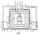
- the transistor is formed in Si islands 14, 15 and 16 which are supported by polycrystalline silicon 13 via silicon oxide layers 33.
- Each Si island is formed of N-type monocrystalline silicon having an impurity concentration of 2.5 x 1014 cm ⁇ 3 and a thickness of 45 ⁇ m and has an N+-type layer 17 having an impurity concentration of 4 x 1017 cm ⁇ 3 and a thickness of 8 ⁇ m on side and bottom surfaces.
- a P-type ring-shape base region 41 having an impurity concentration of 9 x 1016 cm ⁇ 3 and a depth of 6 ⁇ m is formed in the Si island 14.
- An N+-type ring-shape source region 40 having an impurity concentration of 2.5 x 1018 cm ⁇ 3 and a depth of 3 ⁇ m is formed in the base region 41.
- a gate insulator film 48 of SiO2 having a thickness of 1,000 ⁇ is formed to cover portion surrounded by the ring-shape source region 40 with some coverage over the source region 40.
- a gate electrode 49 of polycrystalline silicon having a thickness of 5,000 ⁇ is formed on the gate insulator film 48 and is covered with SiO2 layer having an aperture to expose a part of the gate electrode 49.
- a gate wiring 7-3 of aluminum is connected to the exposed part of the gate electrode 49 to connect with a gate terminal 52.
- Aluminum source electrode 7-2 contacts both of source and base regions 40 and 41 to connect with a source terminal 1.
- a ring-shape P+-type region 45 having an impurity concentration of 3.5 x 1018 cm ⁇ 3 and a depth of 4 ⁇ m is formed in the island 14 so as to surround but isolated from the base
- P-type resistance regions 18 having an impurity concentration of 1.5 x 1018 cm ⁇ 3 are respectively formed in the islands 15 and 16 by impurity diffusion.
- One end of each resistance region 18 is connected to the N+-type region 17 in the island 14 by an aluminum wiring 7-4 which is isolated from the N+-type regions 17 in the islands 15 and 16 by silicon oxide layer 19.
- the other end of each resistance region 18 is connected to the P+-type region 45 with aluminum drain electrode 7-1 which is connected to drain terminal 3. It is noted that, although two drain terminals 3 are shown, those two drain terminals 3 are used in an application by electrically connecting with each other.
- drain-source voltage V DS When the drain-source voltage V DS is small, since the PN-junction between the P+-type region 5 and the N-type island 14 is not biased forward, drain current flows through a route of the drain electrode 7-1-the resistance region 18-the aluminum wiring 7-4-the N+-type region 17 in the island 14-the island 14-the base region 41 under the gate electrode 49-the source region 40-the source electrode 72. Therefore, the transistor operates as a MOS field effect transistor. As the drain-source voltage V DS increases, the drain current rises to increase the voltage drop across the resistance region 18.
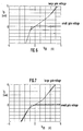
- Fig. 4 shows a relationship between the drain current I D and the drain-source voltage V DS of the prior art IGT in which a one conductivity-type Si substrate has another conductivity-type region on all over the bottom surface as disclosed in IEDM83, pages 83 to 86.
- the drain current I D stops flowing in the drain-source voltage range below 0.7 volts.
- the drain current I D of the transistor shown in Figs. 2 and 3 flows at the drain-source voltage range below 0.7 volts, as shown in Figs. 5, 6 and 7.
- Fig. 4 shows a relationship between the drain current I D and the drain-source voltage V DS of the prior art IGT in which a one conductivity-type Si substrate has another conductivity-type region on all over the bottom surface as disclosed in IEDM83, pages 83 to 86.
- the drain current I D stops flowing in the drain-source voltage range below 0.7 volts.
- the drain current I D of the transistor shown in Figs. 2 and 3 flows at the drain-source
- Fig. 5 is a case of the transistor having the resistance region 18 of 15 ohms and shows a turning point between MOS and IGT operations at the drain-source voltage V DS of about 2.8 volts.
- Fig. 6 is a case having the resistance region 18 of 20 ohms and shows the turning point at about 2.4 volts.
- Fig. 7 is a case having the resistance region 18 of 39 ohms and shows the turning point at about 1.5 volts.
- the turning point between MOS and IGT operations lowers with increment of the resistance of the resistance region 18. This means the turning point may be arbitrarily controlled by adjusting the resistance of the resistance region 18.
- the resistance of the resistance region 18, however, should be selected in a range from 1/10 to 10 times of ON-resistance of the transistor operating as the MOS field effect transistor.
- Figs. 8(a) and 8(b) are input and output waveforms of the prior art IGT as disclosed in IEDM 83 pages 83 to 86.
- the output waveform is deformed at its leading edges corresponding to the off-condition of the IGT just after changed from on-condition. This is because, when the IGT turns off, charges in the island 14 lose their discharging path and disappear by recombination in the island 14.
- the transistor according to the preferred embodiment shows input and output waveforms shown in Figs. 9(a) and 9(b).
- the output waveform has a sharp leading edges. This result shows a high speed operation. More specifically, the drain electrode 7-1 is connected to the N+-type region 17 in the island 14 through the resistance region 18. Therefore, if the transistor turns off, the charges in the island 14 can quickly discharge through the N+-type region 17 in the island 14 and the resistance region 18, resulted in a quick risinging of the output signal.
- the preferred embodiment can be formed in a single monocrystalline silicon chip with using islands isolated from each other by means of PN-junction isolation.
- the resistance regions 18 in the second preferred embodiment may be formed with resistive metal deposited on the field oxide layer.
Landscapes
- Insulated Gate Type Field-Effect Transistor (AREA)
- Bipolar Transistors (AREA)
Applications Claiming Priority (2)
| Application Number | Priority Date | Filing Date | Title |
|---|---|---|---|
| JP248311/87 | 1987-09-30 | ||
| JP62248311A JPH0680832B2 (ja) | 1987-09-30 | 1987-09-30 | 半導体装置 |
Related Parent Applications (1)
| Application Number | Title | Priority Date | Filing Date |
|---|---|---|---|
| EP88116192.1 Division | 1988-09-30 |
Publications (2)
| Publication Number | Publication Date |
|---|---|
| EP0478004A2 true EP0478004A2 (de) | 1992-04-01 |
| EP0478004A3 EP0478004A3 (en) | 1992-05-06 |
Family
ID=17176187
Family Applications (2)
| Application Number | Title | Priority Date | Filing Date |
|---|---|---|---|
| EP19910119868 Withdrawn EP0478004A3 (en) | 1987-09-30 | 1988-09-30 | Insulated gate transistor operable at a low drain-source voltage |
| EP88116192A Expired EP0310112B1 (de) | 1987-09-30 | 1988-09-30 | Isolierter Gate-Transistor, verwendbar bei niedriger Drain-Source-Spannung |
Family Applications After (1)
| Application Number | Title | Priority Date | Filing Date |
|---|---|---|---|
| EP88116192A Expired EP0310112B1 (de) | 1987-09-30 | 1988-09-30 | Isolierter Gate-Transistor, verwendbar bei niedriger Drain-Source-Spannung |
Country Status (4)
| Country | Link |
|---|---|
| US (1) | US5060032A (de) |
| EP (2) | EP0478004A3 (de) |
| JP (1) | JPH0680832B2 (de) |
| DE (1) | DE3876359T2 (de) |
Cited By (1)
| Publication number | Priority date | Publication date | Assignee | Title |
|---|---|---|---|---|
| EP0649175A1 (de) * | 1993-10-15 | 1995-04-19 | Siemens Aktiengesellschaft | Laterales IGBT-Bauteil mit schaltbarer Anodenstruktur |
Families Citing this family (8)
| Publication number | Priority date | Publication date | Assignee | Title |
|---|---|---|---|---|
| JPH0680832B2 (ja) | 1987-09-30 | 1994-10-12 | 日本電気株式会社 | 半導体装置 |
| US5198688A (en) * | 1989-03-06 | 1993-03-30 | Fuji Electric Co., Ltd. | Semiconductor device provided with a conductivity modulation MISFET |
| JP3182262B2 (ja) * | 1993-07-12 | 2001-07-03 | 株式会社東芝 | 半導体装置 |
| US5665988A (en) * | 1995-02-09 | 1997-09-09 | Fuji Electric Co., Ltd. | Conductivity-modulation semiconductor |
| JP2005333055A (ja) * | 2004-05-21 | 2005-12-02 | Toyota Central Res & Dev Lab Inc | 半導体装置 |
| JP2006332199A (ja) * | 2005-05-24 | 2006-12-07 | Shindengen Electric Mfg Co Ltd | SiC半導体装置 |
| JP4937213B2 (ja) * | 2008-08-26 | 2012-05-23 | 三菱電機株式会社 | 電力用半導体装置 |
| JP2012186353A (ja) * | 2011-03-07 | 2012-09-27 | Fuji Electric Co Ltd | 複合半導体装置 |
Citations (2)
| Publication number | Priority date | Publication date | Assignee | Title |
|---|---|---|---|---|
| JPS60170263A (ja) | 1984-02-15 | 1985-09-03 | Nec Corp | 縦型電界効果トランジスタ |
| EP0310112A2 (de) | 1987-09-30 | 1989-04-05 | Nec Corporation | Isolierter Gate-Transistor, verwendbar bei niedriger Drain-Source-Spannung |
Family Cites Families (6)
| Publication number | Priority date | Publication date | Assignee | Title |
|---|---|---|---|---|
| JPS5864059A (ja) * | 1981-10-14 | 1983-04-16 | Hitachi Ltd | 高耐圧抵抗素子 |
| EP0118007B1 (de) * | 1983-02-04 | 1990-05-23 | General Electric Company | Elektrische Schaltung eine hybride Leistungsschalthalbleiteranordnung mit SCR-Struktur enthaltend |
| JPS6017026A (ja) * | 1983-07-08 | 1985-01-28 | Nishimura Watanabe Chiyuushiyutsu Kenkyusho:Kk | 金属チタンの製造方法 |
| DE3628857A1 (de) * | 1985-08-27 | 1987-03-12 | Mitsubishi Electric Corp | Halbleitereinrichtung |
| CA1252225A (en) * | 1985-11-27 | 1989-04-04 | Sel Colak | Lateral insulated gate transistors with coupled anode and gate regions |
| US4901127A (en) * | 1988-10-07 | 1990-02-13 | General Electric Company | Circuit including a combined insulated gate bipolar transistor/MOSFET |
-
1987
- 1987-09-30 JP JP62248311A patent/JPH0680832B2/ja not_active Expired - Lifetime
-
1988
- 1988-09-30 DE DE8888116192T patent/DE3876359T2/de not_active Expired - Fee Related
- 1988-09-30 EP EP19910119868 patent/EP0478004A3/en not_active Withdrawn
- 1988-09-30 EP EP88116192A patent/EP0310112B1/de not_active Expired
-
1990
- 1990-11-13 US US07/611,453 patent/US5060032A/en not_active Expired - Fee Related
Patent Citations (2)
| Publication number | Priority date | Publication date | Assignee | Title |
|---|---|---|---|---|
| JPS60170263A (ja) | 1984-02-15 | 1985-09-03 | Nec Corp | 縦型電界効果トランジスタ |
| EP0310112A2 (de) | 1987-09-30 | 1989-04-05 | Nec Corporation | Isolierter Gate-Transistor, verwendbar bei niedriger Drain-Source-Spannung |
Non-Patent Citations (2)
| Title |
|---|
| M. F. CHANG ET AL., IEDM83, pages 83 - 86 |
| M.R. SIMPSON, IEDM85, pages 740 - 743 |
Cited By (2)
| Publication number | Priority date | Publication date | Assignee | Title |
|---|---|---|---|---|
| EP0649175A1 (de) * | 1993-10-15 | 1995-04-19 | Siemens Aktiengesellschaft | Laterales IGBT-Bauteil mit schaltbarer Anodenstruktur |
| US5519241A (en) * | 1993-10-15 | 1996-05-21 | Siemens Aktiengesellschaft | Circuit structure having at least one bipolar power component and method for the operation thereof |
Also Published As
| Publication number | Publication date |
|---|---|
| DE3876359D1 (de) | 1993-01-14 |
| EP0310112B1 (de) | 1992-12-02 |
| EP0310112A3 (en) | 1989-05-24 |
| EP0478004A3 (en) | 1992-05-06 |
| DE3876359T2 (de) | 1993-04-01 |
| US5060032A (en) | 1991-10-22 |
| EP0310112A2 (de) | 1989-04-05 |
| JPH0680832B2 (ja) | 1994-10-12 |
| JPS6489564A (en) | 1989-04-04 |
Similar Documents
| Publication | Publication Date | Title |
|---|---|---|
| JP4129306B2 (ja) | 電界効果によって制御可能な縦形半導体デバイス及びその製造方法 | |
| US4689647A (en) | Conductivity modulated field effect switch with optimized anode emitter and anode base impurity concentrations | |
| US5801431A (en) | MOS gated semiconductor device with source metal covering the active gate | |
| EP0144909B1 (de) | Integrierte Leistungshalbleiterschaltanordnungen mit IGT- und MOSFET-Strukturen | |
| US4969028A (en) | Gate enhanced rectifier | |
| US6528826B2 (en) | Depletion type MOS semiconductor device and MOS power IC | |
| US8124983B2 (en) | Power transistor | |
| US5777367A (en) | Integrated structure active clamp for the protection of power devices against overvoltages | |
| US5910664A (en) | Emitter-switched transistor structures | |
| US4782379A (en) | Semiconductor device having rapid removal of majority carriers from an active base region thereof at device turn-off and method of fabricating this device | |
| CN117096190A (zh) | 具有高dv/dt能力的功率开关装置及制造这种装置的方法 | |
| EP0503605B1 (de) | Bipolarer Transistor vom isolierten Gatetyp mit Überspannungschutz | |
| CA1225164A (en) | Integrated field controlled thyristor structure with grounded cathode | |
| EP0338312B1 (de) | Bipolarer Transistor mit isolierter Steuerelektrode | |
| EP1044474A1 (de) | Graben-gate-halbleiteranordnung | |
| EP0478004A2 (de) | Transistor mit isolierter Steuerelektrode mit niedriger Drain-Source Betriebsspannung | |
| EP0014080B1 (de) | Halbleiterschaltungs-Vorrichtung mit drei Klemmen | |
| EP0630054A1 (de) | Thyristor mit isolierten Gate und Methode, derselben zu Betreiben | |
| US5587595A (en) | Lateral field-effect-controlled semiconductor device on insulating substrate | |
| CA1173568A (en) | Semiconductor device | |
| US5455442A (en) | COMFET switch and method | |
| JPH09181315A (ja) | 半導体デバイス | |
| EP0540017A1 (de) | MOS-Gate-kontrollierter Thyristor | |
| US20240413229A1 (en) | Semiconductor device having first trenches with a gate electrode and second trenches with a source electrode | |
| US4969024A (en) | Metal-oxide-semiconductor device |
Legal Events
| Date | Code | Title | Description |
|---|---|---|---|
| PUAI | Public reference made under article 153(3) epc to a published international application that has entered the european phase |
Free format text: ORIGINAL CODE: 0009012 |
|
| PUAL | Search report despatched |
Free format text: ORIGINAL CODE: 0009013 |
|
| 17P | Request for examination filed |
Effective date: 19911121 |
|
| AC | Divisional application: reference to earlier application |
Ref document number: 310112 Country of ref document: EP |
|
| AK | Designated contracting states |
Kind code of ref document: A2 Designated state(s): DE FR GB |
|
| AK | Designated contracting states |
Kind code of ref document: A3 Designated state(s): DE FR GB |
|
| 17Q | First examination report despatched |
Effective date: 19941011 |
|
| STAA | Information on the status of an ep patent application or granted ep patent |
Free format text: STATUS: THE APPLICATION HAS BEEN WITHDRAWN |
|
| 18W | Application withdrawn |
Withdrawal date: 19950419 |