EP0478908A1 - Procédé et appareillage pour le traitement réactif d'objets au moyen d'une décharge, luminescente en courant continu - Google Patents
Procédé et appareillage pour le traitement réactif d'objets au moyen d'une décharge, luminescente en courant continu Download PDFInfo
- Publication number
- EP0478908A1 EP0478908A1 EP91112187A EP91112187A EP0478908A1 EP 0478908 A1 EP0478908 A1 EP 0478908A1 EP 91112187 A EP91112187 A EP 91112187A EP 91112187 A EP91112187 A EP 91112187A EP 0478908 A1 EP0478908 A1 EP 0478908A1
- Authority
- EP
- European Patent Office
- Prior art keywords
- arrangement
- recipient
- inlet
- distribution
- suction
- Prior art date
- Legal status (The legal status is an assumption and is not a legal conclusion. Google has not performed a legal analysis and makes no representation as to the accuracy of the status listed.)
- Granted
Links
- 238000000034 method Methods 0.000 title claims abstract description 65
- 238000009826 distribution Methods 0.000 claims abstract description 47
- 238000011282 treatment Methods 0.000 claims abstract description 34
- 238000010891 electric arc Methods 0.000 claims abstract description 32
- 239000002245 particle Substances 0.000 claims abstract description 12
- 239000000463 material Substances 0.000 claims description 30
- 238000006243 chemical reaction Methods 0.000 claims description 24
- 230000000694 effects Effects 0.000 claims description 8
- 239000000203 mixture Substances 0.000 claims description 5
- 230000033228 biological regulation Effects 0.000 claims description 4
- 239000007795 chemical reaction product Substances 0.000 claims description 4
- 230000008878 coupling Effects 0.000 claims description 4
- 238000010168 coupling process Methods 0.000 claims description 4
- 238000005859 coupling reaction Methods 0.000 claims description 4
- 238000007667 floating Methods 0.000 claims description 4
- 238000009434 installation Methods 0.000 claims description 4
- 238000009489 vacuum treatment Methods 0.000 claims description 4
- 239000002800 charge carrier Substances 0.000 claims description 3
- 230000006735 deficit Effects 0.000 claims 1
- 238000009832 plasma treatment Methods 0.000 claims 1
- 210000002381 plasma Anatomy 0.000 abstract description 27
- 238000002347 injection Methods 0.000 abstract description 2
- 239000007924 injection Substances 0.000 abstract description 2
- 238000004381 surface treatment Methods 0.000 abstract 1
- 239000007789 gas Substances 0.000 description 58
- 238000000576 coating method Methods 0.000 description 12
- 239000011248 coating agent Substances 0.000 description 10
- 238000010438 heat treatment Methods 0.000 description 8
- 239000000047 product Substances 0.000 description 5
- 239000000758 substrate Substances 0.000 description 5
- 239000000969 carrier Substances 0.000 description 4
- 238000010926 purge Methods 0.000 description 4
- VYPSYNLAJGMNEJ-UHFFFAOYSA-N Silicium dioxide Chemical compound O=[Si]=O VYPSYNLAJGMNEJ-UHFFFAOYSA-N 0.000 description 3
- XKRFYHLGVUSROY-UHFFFAOYSA-N Argon Chemical compound [Ar] XKRFYHLGVUSROY-UHFFFAOYSA-N 0.000 description 2
- 230000015572 biosynthetic process Effects 0.000 description 2
- 238000001816 cooling Methods 0.000 description 2
- 230000008021 deposition Effects 0.000 description 2
- 230000018109 developmental process Effects 0.000 description 2
- 238000010586 diagram Methods 0.000 description 2
- 238000011010 flushing procedure Methods 0.000 description 2
- 238000009413 insulation Methods 0.000 description 2
- 150000002500 ions Chemical class 0.000 description 2
- 238000004519 manufacturing process Methods 0.000 description 2
- 229910052751 metal Inorganic materials 0.000 description 2
- 239000002184 metal Substances 0.000 description 2
- 229910052756 noble gas Inorganic materials 0.000 description 2
- 239000010453 quartz Substances 0.000 description 2
- 239000000376 reactant Substances 0.000 description 2
- 239000012495 reaction gas Substances 0.000 description 2
- 238000003860 storage Methods 0.000 description 2
- 239000004215 Carbon black (E152) Substances 0.000 description 1
- UFHFLCQGNIYNRP-UHFFFAOYSA-N Hydrogen Chemical compound [H][H] UFHFLCQGNIYNRP-UHFFFAOYSA-N 0.000 description 1
- 229910052786 argon Inorganic materials 0.000 description 1
- 230000004323 axial length Effects 0.000 description 1
- 238000005255 carburizing Methods 0.000 description 1
- 239000000919 ceramic Substances 0.000 description 1
- 229910010293 ceramic material Inorganic materials 0.000 description 1
- 238000001311 chemical methods and process Methods 0.000 description 1
- 239000004020 conductor Substances 0.000 description 1
- 238000011109 contamination Methods 0.000 description 1
- 230000007423 decrease Effects 0.000 description 1
- 230000001419 dependent effect Effects 0.000 description 1
- 239000010432 diamond Substances 0.000 description 1
- 229910003460 diamond Inorganic materials 0.000 description 1
- 238000005516 engineering process Methods 0.000 description 1
- 210000003608 fece Anatomy 0.000 description 1
- 150000004678 hydrides Chemical class 0.000 description 1
- 229930195733 hydrocarbon Natural products 0.000 description 1
- 150000002430 hydrocarbons Chemical class 0.000 description 1
- 239000001257 hydrogen Substances 0.000 description 1
- 229910052739 hydrogen Inorganic materials 0.000 description 1
- 230000007935 neutral effect Effects 0.000 description 1
- 150000002835 noble gases Chemical class 0.000 description 1
- 230000005855 radiation Effects 0.000 description 1
- 239000003870 refractory metal Substances 0.000 description 1
- 229910021332 silicide Inorganic materials 0.000 description 1
- 239000000243 solution Substances 0.000 description 1
- 238000005507 spraying Methods 0.000 description 1
- 229910001220 stainless steel Inorganic materials 0.000 description 1
- 239000010935 stainless steel Substances 0.000 description 1
- 229910052715 tantalum Inorganic materials 0.000 description 1
- GUVRBAGPIYLISA-UHFFFAOYSA-N tantalum atom Chemical compound [Ta] GUVRBAGPIYLISA-UHFFFAOYSA-N 0.000 description 1
- 238000009827 uniform distribution Methods 0.000 description 1
- 238000011144 upstream manufacturing Methods 0.000 description 1
- 238000007740 vapor deposition Methods 0.000 description 1
Images



Classifications
-
- C—CHEMISTRY; METALLURGY
- C23—COATING METALLIC MATERIAL; COATING MATERIAL WITH METALLIC MATERIAL; CHEMICAL SURFACE TREATMENT; DIFFUSION TREATMENT OF METALLIC MATERIAL; COATING BY VACUUM EVAPORATION, BY SPUTTERING, BY ION IMPLANTATION OR BY CHEMICAL VAPOUR DEPOSITION, IN GENERAL; INHIBITING CORROSION OF METALLIC MATERIAL OR INCRUSTATION IN GENERAL
- C23C—COATING METALLIC MATERIAL; COATING MATERIAL WITH METALLIC MATERIAL; SURFACE TREATMENT OF METALLIC MATERIAL BY DIFFUSION INTO THE SURFACE, BY CHEMICAL CONVERSION OR SUBSTITUTION; COATING BY VACUUM EVAPORATION, BY SPUTTERING, BY ION IMPLANTATION OR BY CHEMICAL VAPOUR DEPOSITION, IN GENERAL
- C23C16/00—Chemical coating by decomposition of gaseous compounds, without leaving reaction products of surface material in the coating, i.e. chemical vapour deposition [CVD] processes
- C23C16/44—Chemical coating by decomposition of gaseous compounds, without leaving reaction products of surface material in the coating, i.e. chemical vapour deposition [CVD] processes characterised by the method of coating
- C23C16/455—Chemical coating by decomposition of gaseous compounds, without leaving reaction products of surface material in the coating, i.e. chemical vapour deposition [CVD] processes characterised by the method of coating characterised by the method used for introducing gases into reaction chamber or for modifying gas flows in reaction chamber
- C23C16/45563—Gas nozzles
- C23C16/45565—Shower nozzles
-
- C—CHEMISTRY; METALLURGY
- C23—COATING METALLIC MATERIAL; COATING MATERIAL WITH METALLIC MATERIAL; CHEMICAL SURFACE TREATMENT; DIFFUSION TREATMENT OF METALLIC MATERIAL; COATING BY VACUUM EVAPORATION, BY SPUTTERING, BY ION IMPLANTATION OR BY CHEMICAL VAPOUR DEPOSITION, IN GENERAL; INHIBITING CORROSION OF METALLIC MATERIAL OR INCRUSTATION IN GENERAL
- C23C—COATING METALLIC MATERIAL; COATING MATERIAL WITH METALLIC MATERIAL; SURFACE TREATMENT OF METALLIC MATERIAL BY DIFFUSION INTO THE SURFACE, BY CHEMICAL CONVERSION OR SUBSTITUTION; COATING BY VACUUM EVAPORATION, BY SPUTTERING, BY ION IMPLANTATION OR BY CHEMICAL VAPOUR DEPOSITION, IN GENERAL
- C23C16/00—Chemical coating by decomposition of gaseous compounds, without leaving reaction products of surface material in the coating, i.e. chemical vapour deposition [CVD] processes
- C23C16/44—Chemical coating by decomposition of gaseous compounds, without leaving reaction products of surface material in the coating, i.e. chemical vapour deposition [CVD] processes characterised by the method of coating
- C23C16/50—Chemical coating by decomposition of gaseous compounds, without leaving reaction products of surface material in the coating, i.e. chemical vapour deposition [CVD] processes characterised by the method of coating using electric discharges
- C23C16/503—Chemical coating by decomposition of gaseous compounds, without leaving reaction products of surface material in the coating, i.e. chemical vapour deposition [CVD] processes characterised by the method of coating using electric discharges using DC or AC discharges
-
- Y—GENERAL TAGGING OF NEW TECHNOLOGICAL DEVELOPMENTS; GENERAL TAGGING OF CROSS-SECTIONAL TECHNOLOGIES SPANNING OVER SEVERAL SECTIONS OF THE IPC; TECHNICAL SUBJECTS COVERED BY FORMER USPC CROSS-REFERENCE ART COLLECTIONS [XRACs] AND DIGESTS
- Y10—TECHNICAL SUBJECTS COVERED BY FORMER USPC
- Y10S—TECHNICAL SUBJECTS COVERED BY FORMER USPC CROSS-REFERENCE ART COLLECTIONS [XRACs] AND DIGESTS
- Y10S438/00—Semiconductor device manufacturing: process
- Y10S438/935—Gas flow control
Definitions
- the present invention relates to methods according to the preamble of claim 1 and a system according to the preamble of claim 21.
- a method of the type mentioned or such a system are known from CH-A-664 768.
- US-A-4 851 254 a method for reactive, plasma-supported coating of Gut is known, in which a DC arc discharge is maintained in a vacuum recipient between two immediately adjacent electrodes, with a low voltage below 100 V and relatively high arc currents in the order of magnitude between 50A and 100A.
- the material to be coated is insulated outside the cathode / anode section parallel to the arc discharge.
- a working gas which reacts at least partially, is injected into the plasma through a pipeline, lying opposite the material to be treated with respect to the anode / cathode section.
- reaction space In the case of plasma chemical processes, the reaction space is essentially restricted to an environment of the plasma zone, the extent of which is of the order of the free path length. This in turn is proportional to the reciprocal of the pressure. However, it is generally not possible to lower the pressure to expand the reaction space, since this also reduces the concentration of the reactants.
- the deposition of diamond layers from hydrocarbon / hydrogen mixtures may serve as an example.
- the carburizing of the filaments made of refractory metal is so rapid for such arrangements that they fail due to breakage after 1 to 3 coating cycles. This is unacceptable from a controlled manufacturing standpoint. In other gases, similar problems arise as scaling or the formation of hydrides or silicides.
- a disadvantage of the procedure according to CH-A-664 768 is, on the one hand, that in the treatment recipient in the edge area a linear spraying of working gas with reactive gas to be reacted is carried out or that in the interior of the recipient, viewed over its volume, one inhomogeneous discharge or plasma distribution occurs.
- the present invention now aims to remedy the disadvantages mentioned, starting from the last-mentioned, advantageous sheet production.
- a first method of the type mentioned above is distinguished according to the characterizing part of claim 1, a second method according to that of claim 2 and finally an optimized method according to the wording of claim 3.
- a system according to the invention is distinguished on the one hand according to the characterizing part of claim 21 or that of claim 22, an optimized one according to the wording of claim 23.
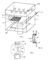
- FIG. 1 schematically shows a first embodiment variant of a treatment chamber according to the invention to explain a first embodiment variant of the procedure according to the invention.
- a vacuum treatment recipient 1 the material 5 to be treated is placed on a holder 3 in the form of one or, as shown, several workpieces.
- the holder 3 defines a storage area for the material to be treated, here a storage level EG.
- the holder 3, and therefore opposite the surface EG, has an inlet arrangement 7 on the recipient 1 for a working gas or gas mixture R with reaction gas or gas mixture.
- the inlet arrangement 7 comprises an area-wide arrangement of inlet openings 9 in a plate 11, which are fed from a pressure compensation chamber 13, which, facing the plate 11 away from the reaction space V of the recipient 1, is itself gas-fed through one or more supply lines 15.
- the holder 3 is designed like a table and is supported on the recipient wall by means of insulation 17. Below the holder 3 there is a suction line 19 for evacuating the recipient 1 and, during the treatment process, for suctioning off gaseous reaction products or used working gas.
- An anode 27 is provided in the recipient 1 opposite the aperture opening 21.
- Hot cathode 25 and anode 27 a DC voltage necessary to maintain an arc discharge B is applied, by means of a DC voltage generator 29.
- the heating of the hot cathode 25 takes place, with electrical heating, by means of a generator 31.
- This generator can be a DC or AC generator, if necessary with a downstream isolating transformer.
- each embodiment is suitable for the cathode of the arc discharge, provided that it is suitable for supplying a sufficiently high current under stable operating conditions.
- the ionization chamber 23 can be replaced by a hollow cathode.
- the ionization chamber is designed as a spark chamber.
- a spark chamber This is shown schematically in Fig. 1. Details of the design of such an assembly are known from vapor deposition technology, where it is already used, for example from DE-OS 34 13 701, which is hereby declared to be an integral part of the present description. 1 schematically shows such a spark chamber with a water-cooled cathode 26, insulation 28, screen 30 and chamber wall 32. The anode is arranged in the chamber.
- the diaphragm 30 or 21, which separates the cathode chamber and the spark chamber from the coating chamber P, must be designed such that on the one hand no metal vapor emerges from the chamber into the coating chamber, and on the other hand the electrons find their way to the anode in the coating chamber.
- the volume of the pressure equalization chamber 13 is so large that there is a uniform pressure distribution of the gas supplied through the line 15 with respect to the inlet openings 9, and by distributing the inlet openings, their flow cross sections and their axial length, and consequently their flow resistance and opening direction specifically effects a desired, essentially directed inflow distribution of the gas into the recipient 1.
- a substantially uniform gas outflow directed against the holder 3 is achieved by uniform distribution and formation of the openings 9 on the plate 11.
- the working gas admitted into the reaction space V partially reacts therein to an increasing extent over time, and used working gas is sucked off through line 19.
- the recipient 1 is preferably formed on all sides from a material which does not impair the treatment process, usually from stainless steel.
- the wall of the recipient 1 can also consist of quartz glass or a ceramic material.
- the holder 3 and consequently the goods are not placed at a specific electrical potential, but, as shown with the insulating supports 17, are operated in a floating manner, so that an electrical potential can be established in accordance with the potential distribution in the reaction space V.
- the treatment temperature of the goods was reduced compared to the case in which the goods were kept at anode potential.
- the arc discharge produced in the manner shown is a long low-voltage discharge which, at pressures of only a few Pa, has a low DC voltage, e.g. below 150V, usually at voltages of the order of magnitude of the ionization energy of the working gas mixture.
- the cathode chamber 23 is preferably, for example, a line 33 , a Purging gas let in.
- the pressure in the cathode chamber 23 can be set so that it is slightly higher than the working pressure in the reaction space V, which results in a gas outflow from the chamber 23.
- a neutral plasma current exits the ionization chamber into the coating chamber, i.e. an equal number of ions as electrons.
- a process-compatible gas usually noble gases, is introduced as the purge gas.
- a plasma with a relatively low gas temperature - at a high electron temperature - can be generated in the range of 2000 C to 1000 ° C. This allows the material to be arranged between the cathode and the anode, as shown in broken lines, which is extremely advantageous for treatment processes which require a high plasma density at low material temperatures.
- the holder 3 is preferably connected to a reference potential, for example anode potential, by a current branch 35, via a resistance element 37. This results in a potential difference based on the impedance conditions in the reaction space V and the value of the resistance element 37 above the latter, and the current 1 driven thereby is used as a temperature control variable for the temperature of the holder and therefore of the material.
- a reference potential for example anode potential
- the potential of the material, decoupled from the arc current can be adjusted by an adjustable voltage source 39 between anode and cathode potential in space V. These procedures are particularly suitable for fine adjustment or regulation of the material temperature.
- the resistance value is adjusted around an operating point.
- the material temperature is also adjusted by adjusting the material potential, decoupled from the discharge.
- the flowing current I is a measure of the electron current; it can be influenced by resistance or direct potential shift on the substrate.
- the temperature of the holder 3 is tapped, as is now clear to the person skilled in the art, an electrical signal corresponding to it is compared with a setpoint value, and the resistance value of the resistance element 37 and / or voltage value at the voltage source 39 are each set as control elements.
- the temperature of the material can be tracked according to a predetermined time characteristic.
- the suction 19 does not have to be carried out centrally, but can also take place peripherally and / or distributed.
- FIG. 2 A further solution according to the invention is shown in FIG. 2, again using a schematically illustrated arrangement according to the invention.
- the gas inlet is not specifically distributed, but the arc discharge.
- a hot cathode chamber arrangement 23 a which extends along a cuboid wall of the recipient 1, is provided on the treatment recipient 1, here of cubic design, to which the working gas R is supplied via a terminally perforated supply line 41, in this case not distributed over an area.
- One or more hot cathodes 25 are provided therein, with a surface distribution.
- the cathode chamber arrangement 23a which can of course also be separate, appropriately distributed chambers, is connected to the reaction space V of the recipient 1 via a plurality of diaphragm openings 21a.
- the rectangular or square-shaped anode 27a is arranged opposite the screens 21a in the recipient.
- a support grid 3 for goods to be coated 5 is provided transversely to the direction of discharge, the suction device 19 on the parallelepiped side facing the working gas supply 41.
- the several arc discharges, here distributed over a wide area result in a coating that is sufficiently uniform for some applications, despite the non-area-distributed working gas supply. Again, the uniformity can the coating can be influenced by targeted distribution of the discharges. Areas are entered with E3 along which the plasma density is essentially constant, with anodes / cathode sections equally distributed and operated in the same way.
- the spatial plasma distribution in the reaction space V is influenced by targeted areal or spatial distribution and / or control of individual or grouped anodes / cathode sections.
- the spatial long-voltage arc discharges can be used to set the spatial effect distribution either by deliberately distributing the working gas inlet over a specific area or by deliberately distributing the arc discharges spatially, so that, with the desired treatment distribution, large-area goods or many can be treated at the same time. this also in three dimensions.
- the arc discharges can be generated in a distributed manner by means of spark chambers of the type shown in connection with FIG. 1.
- FIG. 3 This procedure is shown in principle in FIG. 3, in which an arc discharge B between a hot cathode arrangement 23b and an anode arrangement 27b takes place in a substantial volume area of a reaction space V b of a recipient 1 b in the same direction C as the consumption direction V defined between the working gas inlet and suction R of the reaction gas.
- Such preferred exemplary embodiments are then shown which, combined, show the procedures according to FIGS. 1, 2 and 3.
- the recipient 1 has a cylinder wall 2, for example made of quartz.
- the reaction space V delimited by the wall 2 is closed on the one hand by the inlet arrangement 7 with openings 9 for fresh working gas R.
- an anode plate 27c with an electrically insulating wall section 8 forms the pressure distribution chamber 13, the fresh working gas R being connected through a line connection 15a with center opening 16 is inserted through the anode plate 27c into the pressure distribution chamber 13.
- a plurality of good carriers or substrate carrier grids 3a are arranged on planes which are essentially perpendicular to the recipient axis A.
- the reaction space V is closed off by an orifice plate 24, with outlet orifices 21 c for the schematically entered arc discharges B.
- the hot cathode chamber 25c is provided adjoining the diaphragm plate 24, in which, for example, a hot cathode coil 25c directly heated with heating current I H rotates on the periphery.
- a low-voltage generator is connected between anode plate 27c and hot cathode 25c.
- flushing gas lines 33c open, whereby a flushing gas, such as argon, is let into the hot cathode area.
- the gas that is let into the area of the hot cathode 25c protects the cathode from the effects of the treatment process. This results in a much longer service life for the hot cathode.
- the hot cathode 25c is surrounded by a coaxial diaphragm 40 with radially directed openings 42. This enables a pressure gradation towards the center.
- the cathode chamber 23c is closed off by a cover part 44, with a central suction line 19c.
- the aperture plate 24 is cooled (not shown), but can also be made of a high-temperature resistant material, such as tantalum or a high-temperature resistant ceramic.
- the diaphragm screen 40 is preferably also made from the same material.
- the plate 7 can be connected directly as an anode, namely when the process allows the plate 7 to be made of metal.
- working gas R is admitted into the reaction space V through the inlet openings 9, preferably uniformly distributed.
- the arc discharge is maintained from, for example, the equally distributed diaphragm openings 21 and, via the openings 9 of the arrangement 7, the anode 27c.
- gaseous reaction products flow through the orifices 21c in countercurrent to the electron flow of the arc outlet dung, and through the central region of the cathode chamber 23c from the suction line 29c.
- the workpieces are e.g. potential-free operated substrate support grid 3a deposited or, for temperature control or regulation via a current branch, as explained with reference to FIG. 1, connected to a reference potential or a control voltage source.
- FIG. 5 shows a currently preferred embodiment variant of a treatment chamber according to the invention in greater detail.
- the reference symbols previously used are used for parts or units already described.
- the actual recipient 1 with wall 2 is closed on one side by the inlet arrangement 7.
- a relatively large-diameter perforated, cooled anode plate 50 is arranged, spaced apart and insulated from the plate 11. Again offset from the anode perforated plate 50, a further perforated plate 52 is arranged for better gas distribution.
- the electrical supply 54 for the anode is provided centrally.
- the pressure distribution chamber is formed here by two pressure stages between the two distribution plates 52 and 11.
- the anode plate 50 is designed to be as little disruptive as possible for the working gas, so as to be “transparent” so as not to disturb its flow on the one hand and to be as little affected by this gas as possible on the other.
- heating elements 58 can be provided outside the recipient 1 or, depending on the power requirement, also cooled shielding plates.
- magnetic coils 60 can optionally be provided outside the recipient and coaxially to the anode / cathode section in order to optimize the plasma distribution in the reaction space V with the product carriers 3a by means of magnetic DC or AC fields.
- the actual recipient with possibly provided heaters 58 is closed off by an outer wall 62.
- FIG. 6 schematically shows a treatment chamber according to the invention, in which both the purge gas, let in through the schematically illustrated inlet 68, and also the working gas, as described, are drawn in peripherally through the feed 15.
- the reference symbols already used are used, with which the arrangement shown here can be readily understood by the person skilled in the art.
- a higher pressure is set in the ionization chamber or cathode chamber than in the treatment room. A particularly effective ionization of the gas is thereby achieved. Because the gas in the ionization chamber 23 is essentially a noble gas, the life of the cathode is significantly increased.
- FIG. 4 schematically shows goods to be treated arranged on the crop carriers 3a, and 70 denotes flow regulators, on the one hand for the working gas supplied via connection 15 and on the other hand for the purge gas supplied via the supply 68.
- the suction takes place at the suction connections 72.
- FIG. 7 shows, schematically, the electrically operated system parts of the arrangement according to the invention. These comprise one or, as shown, a plurality of hot cathodes 25, one or more anodes 27, one or more crop carriers 3 for the crop to be treated.
- the treatment systems shown for reactive, low-voltage arc plasma-assisted processes work with low anode / cathode voltages, for example below 150 V, can be operated with high discharge currents per well carrier area, for example over 4000 A / m 2 , and result in low treatment temperatures, essentially below 900 ° C.
- the high used plasma densities at low treatment temperatures result in a multitude of applications.
Landscapes
- Chemical & Material Sciences (AREA)
- Engineering & Computer Science (AREA)
- Metallurgy (AREA)
- Organic Chemistry (AREA)
- General Chemical & Material Sciences (AREA)
- Chemical Kinetics & Catalysis (AREA)
- Materials Engineering (AREA)
- Mechanical Engineering (AREA)
- Physics & Mathematics (AREA)
- Plasma & Fusion (AREA)
- Physical Or Chemical Processes And Apparatus (AREA)
- Chemical Vapour Deposition (AREA)
- ing And Chemical Polishing (AREA)
- Arc Welding Control (AREA)
- Nonmetallic Welding Materials (AREA)
- Discharge Heating (AREA)
Applications Claiming Priority (2)
| Application Number | Priority Date | Filing Date | Title |
|---|---|---|---|
| DE4029268 | 1990-09-14 | ||
| DE4029268A DE4029268C2 (de) | 1990-09-14 | 1990-09-14 | Verfahren zur gleichspannungs-bogenentladungs-unterstützten, reaktiven Behandlung von Gut und Vakuumbehandlungsanlage zur Durchführung |
Publications (2)
| Publication Number | Publication Date |
|---|---|
| EP0478908A1 true EP0478908A1 (fr) | 1992-04-08 |
| EP0478908B1 EP0478908B1 (fr) | 1995-01-25 |
Family
ID=6414297
Family Applications (1)
| Application Number | Title | Priority Date | Filing Date |
|---|---|---|---|
| EP91112187A Expired - Lifetime EP0478908B1 (fr) | 1990-09-14 | 1991-07-20 | Procédé et appareillage pour le traitement réactif d'objets au moyen d'une décharge, luminescente en courant continu |
Country Status (6)
| Country | Link |
|---|---|
| US (2) | US5336326A (fr) |
| EP (1) | EP0478908B1 (fr) |
| JP (1) | JP3318336B2 (fr) |
| AT (1) | ATE117739T1 (fr) |
| DE (2) | DE4029268C2 (fr) |
| ES (1) | ES2067098T3 (fr) |
Cited By (2)
| Publication number | Priority date | Publication date | Assignee | Title |
|---|---|---|---|---|
| EP0717126A3 (fr) * | 1994-12-16 | 1996-12-18 | Hwang Chul Ju | Appareil de dépÔt chimique en phase vapeur à basse pression |
| EP0863227A1 (fr) * | 1997-03-04 | 1998-09-09 | Tokyo Electron Limited | Méthode et dispositif pour la production des couches minces laminées |
Families Citing this family (48)
| Publication number | Priority date | Publication date | Assignee | Title |
|---|---|---|---|---|
| US5565249A (en) * | 1992-05-07 | 1996-10-15 | Fujitsu Limited | Method for producing diamond by a DC plasma jet |
| CH687111A5 (de) * | 1992-05-26 | 1996-09-13 | Balzers Hochvakuum | Verfahren zum Erzeugen einer Niederspannungsentladung, Vakuumbehandlungsanlage hierfuer sowie Anwendung des Verfahrens. |
| US7264850B1 (en) | 1992-12-28 | 2007-09-04 | Semiconductor Energy Laboratory Co., Ltd. | Process for treating a substrate with a plasma |
| US6001431A (en) * | 1992-12-28 | 1999-12-14 | Semiconductor Energy Laboratory Co., Ltd. | Process for fabricating a magnetic recording medium |
| CA2126731A1 (fr) * | 1993-07-12 | 1995-01-13 | Frank Jansen | Reseau de cathodes creuses et methode de nettoyage de feuilles avec ce reseau |
| JP3146112B2 (ja) * | 1993-12-24 | 2001-03-12 | シャープ株式会社 | プラズマcvd装置 |
| US6200389B1 (en) | 1994-07-18 | 2001-03-13 | Silicon Valley Group Thermal Systems Llc | Single body injector and deposition chamber |
| TW359943B (en) * | 1994-07-18 | 1999-06-01 | Silicon Valley Group Thermal | Single body injector and method for delivering gases to a surface |
| US6022414A (en) * | 1994-07-18 | 2000-02-08 | Semiconductor Equipment Group, Llc | Single body injector and method for delivering gases to a surface |
| EP0724026B1 (fr) * | 1995-01-25 | 1999-10-13 | Balzers Aktiengesellschaft | Procédé de dépÔt réactif |
| US5753045A (en) * | 1995-01-25 | 1998-05-19 | Balzers Aktiengesellschaft | Vacuum treatment system for homogeneous workpiece processing |
| US5772770A (en) * | 1995-01-27 | 1998-06-30 | Kokusai Electric Co, Ltd. | Substrate processing apparatus |
| US5660639A (en) * | 1995-10-17 | 1997-08-26 | Ford Motor Company | Method and apparatus for plasma treating an article |
| TW356554B (en) * | 1995-10-23 | 1999-04-21 | Watkins Johnson Co | Gas injection system for semiconductor processing |
| CH692446A5 (de) | 1996-04-15 | 2002-06-28 | Esec Sa | Verfahren zur Herstellung von Werkstücken und von Teilen hierfür |
| US5906683A (en) * | 1996-04-16 | 1999-05-25 | Applied Materials, Inc. | Lid assembly for semiconductor processing chamber |
| DE19705884A1 (de) * | 1997-02-15 | 1998-08-20 | Leybold Ag | Plasma-Zündvorrichtung |
| US20020011215A1 (en) | 1997-12-12 | 2002-01-31 | Goushu Tei | Plasma treatment apparatus and method of manufacturing optical parts using the same |
| US6892669B2 (en) * | 1998-02-26 | 2005-05-17 | Anelva Corporation | CVD apparatus |
| US5997649A (en) * | 1998-04-09 | 1999-12-07 | Tokyo Electron Limited | Stacked showerhead assembly for delivering gases and RF power to a reaction chamber |
| DE19958016B4 (de) * | 1998-12-02 | 2013-07-18 | Stefan Laure | Plasmagenerator |
| US6250250B1 (en) * | 1999-03-18 | 2001-06-26 | Yuri Maishev | Multiple-cell source of uniform plasma |
| JP3366301B2 (ja) * | 1999-11-10 | 2003-01-14 | 日本電気株式会社 | プラズマcvd装置 |
| US6502530B1 (en) * | 2000-04-26 | 2003-01-07 | Unaxis Balzers Aktiengesellschaft | Design of gas injection for the electrode in a capacitively coupled RF plasma reactor |
| KR100419756B1 (ko) * | 2000-06-23 | 2004-02-21 | 아넬바 가부시기가이샤 | 박막 형성 장치 |
| JP4791637B2 (ja) * | 2001-01-22 | 2011-10-12 | キヤノンアネルバ株式会社 | Cvd装置とこれを用いた処理方法 |
| US6444945B1 (en) | 2001-03-28 | 2002-09-03 | Cp Films, Inc. | Bipolar plasma source, plasma sheet source, and effusion cell utilizing a bipolar plasma source |
| US6537928B1 (en) * | 2002-02-19 | 2003-03-25 | Asm Japan K.K. | Apparatus and method for forming low dielectric constant film |
| US20030124842A1 (en) * | 2001-12-27 | 2003-07-03 | Applied Materials, Inc. | Dual-gas delivery system for chemical vapor deposition processes |
| US6902774B2 (en) | 2002-07-25 | 2005-06-07 | Inficon Gmbh | Method of manufacturing a device |
| US20040031565A1 (en) * | 2002-08-13 | 2004-02-19 | Taiwan Semiconductor Manufacturing Co., Ltd. | Gas distribution plate for processing chamber |
| US7855513B2 (en) * | 2004-09-28 | 2010-12-21 | Old Dominion University Research Foundation | Device and method for gas treatment using pulsed corona discharges |
| US7298092B2 (en) * | 2004-09-28 | 2007-11-20 | Old Dominion University Research Foundation | Device and method for gas treatment using pulsed corona discharges |
| JP2007191792A (ja) * | 2006-01-19 | 2007-08-02 | Atto Co Ltd | ガス分離型シャワーヘッド |
| JPWO2007123102A1 (ja) | 2006-04-18 | 2009-09-03 | 株式会社アルバック | 成膜装置、バリア膜製造方法 |
| JP4867995B2 (ja) * | 2006-12-20 | 2012-02-01 | 株式会社島津製作所 | イオン化装置 |
| WO2009057223A1 (fr) * | 2007-11-02 | 2009-05-07 | Canon Anelva Corporation | Appareil de traitement de surface et procédé de traitement de substrat |
| US8721836B2 (en) * | 2008-04-22 | 2014-05-13 | Micron Technology, Inc. | Plasma processing with preionized and predissociated tuning gases and associated systems and methods |
| JP5274918B2 (ja) | 2008-07-07 | 2013-08-28 | 東京エレクトロン株式会社 | プラズマ処理装置のチャンバー内部材の温度制御方法、チャンバー内部材及び基板載置台、並びにそれを備えたプラズマ処理装置 |
| US8168268B2 (en) * | 2008-12-12 | 2012-05-01 | Ovishinsky Innovation, LLC | Thin film deposition via a spatially-coordinated and time-synchronized process |
| US9761424B1 (en) | 2011-09-07 | 2017-09-12 | Nano-Product Engineering, LLC | Filtered cathodic arc method, apparatus and applications thereof |
| US10304665B2 (en) | 2011-09-07 | 2019-05-28 | Nano-Product Engineering, LLC | Reactors for plasma-assisted processes and associated methods |
| JP2014070233A (ja) * | 2012-09-28 | 2014-04-21 | Toppan Printing Co Ltd | 成膜装置、ガスバリア性積層体および光学部材 |
| US9416450B2 (en) * | 2012-10-24 | 2016-08-16 | Applied Materials, Inc. | Showerhead designs of a hot wire chemical vapor deposition (HWCVD) chamber |
| DE102013225608A1 (de) * | 2013-12-11 | 2015-06-11 | Apo Gmbh Massenkleinteilbeschichtung | Vorrichtung und Verfahren zur Oberflächenbehandlung von Kleinteilen mittels Plasma |
| DE102015101294A1 (de) * | 2015-01-29 | 2016-08-04 | Fraunhofer-Gesellschaft zur Förderung der angewandten Forschung e.V. | Vorrichtung zum Erzeugen eines Hohlkathodenbogenentladungsplasmas |
| KR20170127724A (ko) * | 2016-05-12 | 2017-11-22 | 삼성전자주식회사 | 플라즈마 처리 장치 |
| US11834204B1 (en) | 2018-04-05 | 2023-12-05 | Nano-Product Engineering, LLC | Sources for plasma assisted electric propulsion |
Citations (4)
| Publication number | Priority date | Publication date | Assignee | Title |
|---|---|---|---|---|
| EP0115970A1 (fr) * | 1983-01-05 | 1984-08-15 | Commissariat A L'energie Atomique | Enceinte pour le traitement et notamment la gravure de substrats par la méthode du plasma réactif |
| GB2176808A (en) * | 1985-06-20 | 1987-01-07 | Balzers Hochvakuum | A method of coating substrates in a vacuum chamber |
| GB2178228A (en) * | 1985-07-01 | 1987-02-04 | Balzers Hochvakuum | An arrangement for the treating of workpieces |
| US4731255A (en) * | 1984-09-26 | 1988-03-15 | Applied Materials Japan, Inc. | Gas-phase growth process and an apparatus for the same |
Family Cites Families (10)
| Publication number | Priority date | Publication date | Assignee | Title |
|---|---|---|---|---|
| FR2397067A1 (fr) * | 1977-07-06 | 1979-02-02 | Commissariat Energie Atomique | Dispositif d'injection de gaz pour gravure ou depot reactifs sous decharge luminescente |
| JPS5893241A (ja) * | 1981-11-30 | 1983-06-02 | Sony Corp | 半導体装置 |
| JPS6063919A (ja) * | 1983-09-17 | 1985-04-12 | Anelva Corp | 表面処理装置 |
| US4556471A (en) * | 1983-10-14 | 1985-12-03 | Multi-Arc Vacuum Systems Inc. | Physical vapor deposition apparatus |
| US4859490A (en) * | 1986-07-23 | 1989-08-22 | Sumitomo Electric Industries, Ltd. | Method for synthesizing diamond |
| US4851254A (en) * | 1987-01-13 | 1989-07-25 | Nippon Soken, Inc. | Method and device for forming diamond film |
| DE3820249A1 (de) * | 1988-06-14 | 1989-12-21 | Swarovski & Co | Fassung fuer schmucksteine |
| DE3830249A1 (de) * | 1988-09-06 | 1990-03-15 | Schott Glaswerke | Plasmaverfahren zum beschichten ebener substrate |
| JPH02101740A (ja) * | 1988-10-11 | 1990-04-13 | Anelva Corp | プラズマエッチング装置 |
| JPH03207859A (ja) * | 1990-01-10 | 1991-09-11 | Hitachi Ltd | イオン源装置およびイオンビーム処理装置 |
-
1990
- 1990-09-14 DE DE4029268A patent/DE4029268C2/de not_active Expired - Fee Related
-
1991
- 1991-07-20 DE DE59104387T patent/DE59104387D1/de not_active Expired - Lifetime
- 1991-07-20 AT AT91112187T patent/ATE117739T1/de not_active IP Right Cessation
- 1991-07-20 EP EP91112187A patent/EP0478908B1/fr not_active Expired - Lifetime
- 1991-07-20 ES ES91112187T patent/ES2067098T3/es not_active Expired - Lifetime
- 1991-09-11 JP JP23204991A patent/JP3318336B2/ja not_active Expired - Fee Related
- 1991-09-11 US US07/757,712 patent/US5336326A/en not_active Expired - Fee Related
-
1994
- 1994-04-04 US US08/222,378 patent/US5554255A/en not_active Expired - Lifetime
Patent Citations (4)
| Publication number | Priority date | Publication date | Assignee | Title |
|---|---|---|---|---|
| EP0115970A1 (fr) * | 1983-01-05 | 1984-08-15 | Commissariat A L'energie Atomique | Enceinte pour le traitement et notamment la gravure de substrats par la méthode du plasma réactif |
| US4731255A (en) * | 1984-09-26 | 1988-03-15 | Applied Materials Japan, Inc. | Gas-phase growth process and an apparatus for the same |
| GB2176808A (en) * | 1985-06-20 | 1987-01-07 | Balzers Hochvakuum | A method of coating substrates in a vacuum chamber |
| GB2178228A (en) * | 1985-07-01 | 1987-02-04 | Balzers Hochvakuum | An arrangement for the treating of workpieces |
Non-Patent Citations (1)
| Title |
|---|
| PATENT ABSTRACTS OF JAPAN vol. 9, no. 271 (C-311)(1994) 29. Oktober 1985 & JP-A-60 118 693 ( MITSUBISHI KINZOKU K.K. ) 26. Juni 1985 * |
Cited By (8)
| Publication number | Priority date | Publication date | Assignee | Title |
|---|---|---|---|---|
| EP0717126A3 (fr) * | 1994-12-16 | 1996-12-18 | Hwang Chul Ju | Appareil de dépÔt chimique en phase vapeur à basse pression |
| US5928427A (en) * | 1994-12-16 | 1999-07-27 | Hwang; Chul-Ju | Apparatus for low pressure chemical vapor deposition |
| US6009831A (en) * | 1994-12-16 | 2000-01-04 | Hwang; Chul-Ju | Apparatus for low pressure chemical vapor deposition |
| US6026764A (en) * | 1994-12-16 | 2000-02-22 | Hwang; Chul-Ju | Apparatus for low pressure chemical vapor deposition |
| US6190460B1 (en) | 1994-12-16 | 2001-02-20 | Chul-Ju Hwang | Apparatus for low pressure chemical vapor depostion |
| EP0863227A1 (fr) * | 1997-03-04 | 1998-09-09 | Tokyo Electron Limited | Méthode et dispositif pour la production des couches minces laminées |
| US6022586A (en) * | 1997-03-04 | 2000-02-08 | Tokyo Electron Limited | Method and apparatus for forming laminated thin films or layers |
| US6251188B1 (en) | 1997-03-04 | 2001-06-26 | Tokyo Electron Limited | Apparatus for forming laminated thin films or layers |
Also Published As
| Publication number | Publication date |
|---|---|
| JPH04232276A (ja) | 1992-08-20 |
| US5554255A (en) | 1996-09-10 |
| JP3318336B2 (ja) | 2002-08-26 |
| ES2067098T3 (es) | 1995-03-16 |
| DE59104387D1 (de) | 1995-03-09 |
| DE4029268A1 (de) | 1992-03-19 |
| US5336326A (en) | 1994-08-09 |
| DE4029268C2 (de) | 1995-07-06 |
| ATE117739T1 (de) | 1995-02-15 |
| EP0478908B1 (fr) | 1995-01-25 |
Similar Documents
| Publication | Publication Date | Title |
|---|---|---|
| EP0478908B1 (fr) | Procédé et appareillage pour le traitement réactif d'objets au moyen d'une décharge, luminescente en courant continu | |
| EP0478909B1 (fr) | Procédé et appareillage pour la fabrication d'une couche de diamant | |
| DE3875815T2 (de) | Methode zur behandlung der substratoberflaechen mit hilfe von plasma und reaktor fuer die durchfuehrung dieser methode. | |
| EP0275018B1 (fr) | Procédé et appareil pour le revêtement de pièces conductrices par une décharge à arc | |
| EP0727508B1 (fr) | Procédé et appareil de traitement de surfaces de substrats | |
| DE4345602B4 (de) | Verfahren zum Zünden und Betreiben einer Niederspannungs-Bogenentladung, Vakuumbehandlungsanlage und Kathodenkammer hierfür sowie Verwendung des Verfahrens | |
| DE3614384A1 (de) | Verfahren zur beschichtung von substraten in einer vakuumkammer | |
| EP2633543A1 (fr) | Dispositif de production d'un faisceau électronique | |
| EP0881865B1 (fr) | Dispositif de production d'une pluralité de jets de plasma basse température | |
| DE19943064A1 (de) | Verfahren und Vorrichtung zur epitaktischen Abscheidung von Atomen oder Molekülen aus einem Reaktivgas auf einer Abscheidungsoberfläche eines Substrats | |
| WO2000016374A1 (fr) | Dispositif de separation au plasma d'un diamant polycristallin | |
| DE19546827C2 (de) | Einrichtung zur Erzeugung dichter Plasmen in Vakuumprozessen | |
| EP0938595A1 (fr) | Procede et dispositif pour l'enduction de substrats par pulverisation d'un flux gazeux | |
| DE69110547T2 (de) | Plasma-CVD-Anlage. | |
| EP0867036B1 (fr) | Procede et dispositif pour le pretraitement de substrats | |
| DE102013107659B4 (de) | Plasmachemische Beschichtungsvorrichtung | |
| EP0647961A1 (fr) | Dispositif pour le revêtement de produits allongés et susceptibles d'être courbés | |
| DE19727857C1 (de) | Plasmarektor mit Prallströmung zur Oberflächenbehandlung | |
| DE102005049266B4 (de) | Vorrichtung und Verfahren zur Plasmabehandlung von Objekten | |
| EP0791226B1 (fr) | Dispositif pour le recouvrement de substrats au moyen d'un materiau en phase vapeur, sous pression reduite ou sous vide | |
| DE3303677A1 (de) | Plasmakanone | |
| DE10141142B4 (de) | Einrichtung zur reaktiven Plasmabehandlung von Substraten und Verfahren zur Anwendung | |
| DE102014112671A1 (de) | Magnetronanordnung, Prozessieranordnung und Verfahren zum reaktiven Sputtern | |
| DE3222327A1 (de) | Einrichtung zur vakuumbedampfung | |
| CH633729A5 (en) | Device for coating products |
Legal Events
| Date | Code | Title | Description |
|---|---|---|---|
| PUAI | Public reference made under article 153(3) epc to a published international application that has entered the european phase |
Free format text: ORIGINAL CODE: 0009012 |
|
| AK | Designated contracting states |
Kind code of ref document: A1 Designated state(s): AT CH DE ES FR GB IT LI NL SE |
|
| 17P | Request for examination filed |
Effective date: 19920320 |
|
| 17Q | First examination report despatched |
Effective date: 19931013 |
|
| GRAA | (expected) grant |
Free format text: ORIGINAL CODE: 0009210 |
|
| AK | Designated contracting states |
Kind code of ref document: B1 Designated state(s): AT CH DE ES FR GB IT LI NL SE |
|
| REF | Corresponds to: |
Ref document number: 117739 Country of ref document: AT Date of ref document: 19950215 Kind code of ref document: T |
|
| GBT | Gb: translation of ep patent filed (gb section 77(6)(a)/1977) |
Effective date: 19950124 |
|
| REF | Corresponds to: |
Ref document number: 59104387 Country of ref document: DE Date of ref document: 19950309 |
|
| REG | Reference to a national code |
Ref country code: ES Ref legal event code: FG2A Ref document number: 2067098 Country of ref document: ES Kind code of ref document: T3 |
|
| ET | Fr: translation filed | ||
| ITF | It: translation for a ep patent filed | ||
| PLBE | No opposition filed within time limit |
Free format text: ORIGINAL CODE: 0009261 |
|
| STAA | Information on the status of an ep patent application or granted ep patent |
Free format text: STATUS: NO OPPOSITION FILED WITHIN TIME LIMIT |
|
| 26N | No opposition filed | ||
| REG | Reference to a national code |
Ref country code: GB Ref legal event code: IF02 |
|
| PGFP | Annual fee paid to national office [announced via postgrant information from national office to epo] |
Ref country code: AT Payment date: 20030711 Year of fee payment: 13 |
|
| PGFP | Annual fee paid to national office [announced via postgrant information from national office to epo] |
Ref country code: NL Payment date: 20030730 Year of fee payment: 13 |
|
| PGFP | Annual fee paid to national office [announced via postgrant information from national office to epo] |
Ref country code: ES Payment date: 20030813 Year of fee payment: 13 |
|
| PG25 | Lapsed in a contracting state [announced via postgrant information from national office to epo] |
Ref country code: AT Free format text: LAPSE BECAUSE OF NON-PAYMENT OF DUE FEES Effective date: 20040720 |
|
| PG25 | Lapsed in a contracting state [announced via postgrant information from national office to epo] |
Ref country code: ES Free format text: LAPSE BECAUSE OF NON-PAYMENT OF DUE FEES Effective date: 20040721 |
|
| PG25 | Lapsed in a contracting state [announced via postgrant information from national office to epo] |
Ref country code: NL Free format text: LAPSE BECAUSE OF NON-PAYMENT OF DUE FEES Effective date: 20050201 |
|
| NLV4 | Nl: lapsed or anulled due to non-payment of the annual fee |
Effective date: 20050201 |
|
| PGFP | Annual fee paid to national office [announced via postgrant information from national office to epo] |
Ref country code: SE Payment date: 20050706 Year of fee payment: 15 |
|
| PGFP | Annual fee paid to national office [announced via postgrant information from national office to epo] |
Ref country code: FR Payment date: 20050708 Year of fee payment: 15 |
|
| PG25 | Lapsed in a contracting state [announced via postgrant information from national office to epo] |
Ref country code: IT Free format text: LAPSE BECAUSE OF NON-PAYMENT OF DUE FEES;WARNING: LAPSES OF ITALIAN PATENTS WITH EFFECTIVE DATE BEFORE 2007 MAY HAVE OCCURRED AT ANY TIME BEFORE 2007. THE CORRECT EFFECTIVE DATE MAY BE DIFFERENT FROM THE ONE RECORDED. Effective date: 20050720 |
|
| PGFP | Annual fee paid to national office [announced via postgrant information from national office to epo] |
Ref country code: GB Payment date: 20050720 Year of fee payment: 15 |
|
| REG | Reference to a national code |
Ref country code: ES Ref legal event code: FD2A Effective date: 20040721 |
|
| PGFP | Annual fee paid to national office [announced via postgrant information from national office to epo] |
Ref country code: CH Payment date: 20051017 Year of fee payment: 15 |
|
| PG25 | Lapsed in a contracting state [announced via postgrant information from national office to epo] |
Ref country code: GB Free format text: LAPSE BECAUSE OF NON-PAYMENT OF DUE FEES Effective date: 20060720 |
|
| PG25 | Lapsed in a contracting state [announced via postgrant information from national office to epo] |
Ref country code: SE Free format text: LAPSE BECAUSE OF NON-PAYMENT OF DUE FEES Effective date: 20060721 |
|
| PG25 | Lapsed in a contracting state [announced via postgrant information from national office to epo] |
Ref country code: CH Free format text: LAPSE BECAUSE OF NON-PAYMENT OF DUE FEES Effective date: 20060731 Ref country code: LI Free format text: LAPSE BECAUSE OF NON-PAYMENT OF DUE FEES Effective date: 20060731 |
|
| REG | Reference to a national code |
Ref country code: CH Ref legal event code: PL |
|
| EUG | Se: european patent has lapsed | ||
| GBPC | Gb: european patent ceased through non-payment of renewal fee |
Effective date: 20060720 |
|
| REG | Reference to a national code |
Ref country code: FR Ref legal event code: ST Effective date: 20070330 |
|
| PG25 | Lapsed in a contracting state [announced via postgrant information from national office to epo] |
Ref country code: FR Free format text: LAPSE BECAUSE OF NON-PAYMENT OF DUE FEES Effective date: 20060731 |
|
| PGFP | Annual fee paid to national office [announced via postgrant information from national office to epo] |
Ref country code: DE Payment date: 20100714 Year of fee payment: 20 |
|
| REG | Reference to a national code |
Ref country code: DE Ref legal event code: R071 Ref document number: 59104387 Country of ref document: DE |
|
| REG | Reference to a national code |
Ref country code: DE Ref legal event code: R071 Ref document number: 59104387 Country of ref document: DE |
|
| PG25 | Lapsed in a contracting state [announced via postgrant information from national office to epo] |
Ref country code: DE Free format text: LAPSE BECAUSE OF EXPIRATION OF PROTECTION Effective date: 20110721 |