EP0479213A2 - Méthode et dispositif de traitement non-linéaire - Google Patents
Méthode et dispositif de traitement non-linéaire Download PDFInfo
- Publication number
- EP0479213A2 EP0479213A2 EP91116707A EP91116707A EP0479213A2 EP 0479213 A2 EP0479213 A2 EP 0479213A2 EP 91116707 A EP91116707 A EP 91116707A EP 91116707 A EP91116707 A EP 91116707A EP 0479213 A2 EP0479213 A2 EP 0479213A2
- Authority
- EP
- European Patent Office
- Prior art keywords
- output
- amplifiers
- nonlinear processing
- processing apparatus
- input signal
- Prior art date
- Legal status (The legal status is an assumption and is not a legal conclusion. Google has not performed a legal analysis and makes no representation as to the accuracy of the status listed.)
- Granted
Links
Images





Classifications
-
- H—ELECTRICITY
- H03—ELECTRONIC CIRCUITRY
- H03G—CONTROL OF AMPLIFICATION
- H03G7/00—Volume compression or expansion in amplifiers
- H03G7/001—Volume compression or expansion in amplifiers without controlling loop
-
- H—ELECTRICITY
- H04—ELECTRIC COMMUNICATION TECHNIQUE
- H04N—PICTORIAL COMMUNICATION, e.g. TELEVISION
- H04N9/00—Details of colour television systems
- H04N9/64—Circuits for processing colour signals
- H04N9/68—Circuits for processing colour signals for controlling the amplitude of colour signals, e.g. automatic chroma control circuits
- H04N9/69—Circuits for processing colour signals for controlling the amplitude of colour signals, e.g. automatic chroma control circuits for modifying the colour signals by gamma correction
Definitions
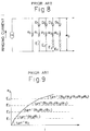
- the frequency responses for the operating portions corresponding to individual line segments which constitute the input/output characteristic cannot be determined independently. For instance, if one tries to perform adjustment to provide the best frequency response in a black level region where the signal lever is low, the adjustment will affect the frequency response in a region where the signal level is high. Therefore this necessitates setting the frequency response in light of a balance over the whole level range, making it difficult to provide the optimal frequency response for each level range.
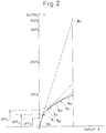
- This method can provide an arbitrary nonlinear output characteristic and can permit independent adjustment of the output characteristic for each selected output signal.
- the frequency responses for the individual line segments cannot independently be determined as is apparent from the above formula of the line inclination. For instance, if one tries to perform adjustment to provide the best frequency response in a black level region where the signal level is low, the adjustment will affect the frequency response in a region where the signal level is high. It is therefore necessary to set the frequency response in light of a balance over the whole level range, so that the optimal frequency response for each level cannot be acquired.
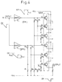
- the characteristics of the individual line segments can be obtained by selectively switching and outputting the outputs of the individual amplifiers from one to another (unlike the prior art wherein the individual outputs of the amplifiers are added to be a final output), the characteristics of the individual line segments can independently be set or adjusted and the dynamic range can be designed narrower even though the circuit is designed as having a same output level.
Landscapes
- Engineering & Computer Science (AREA)
- Multimedia (AREA)
- Signal Processing (AREA)
- Picture Signal Circuits (AREA)
- Processing Of Color Television Signals (AREA)
- Tone Control, Compression And Expansion, Limiting Amplitude (AREA)
- Amplifiers (AREA)
Applications Claiming Priority (2)
| Application Number | Priority Date | Filing Date | Title |
|---|---|---|---|
| JP2263203A JP2554955B2 (ja) | 1990-10-02 | 1990-10-02 | 非線形処理回路 |
| JP263203/90 | 1990-10-02 |
Publications (3)
| Publication Number | Publication Date |
|---|---|
| EP0479213A2 true EP0479213A2 (fr) | 1992-04-08 |
| EP0479213A3 EP0479213A3 (en) | 1992-07-01 |
| EP0479213B1 EP0479213B1 (fr) | 1996-05-01 |
Family
ID=17386214
Family Applications (1)
| Application Number | Title | Priority Date | Filing Date |
|---|---|---|---|
| EP91116707A Expired - Lifetime EP0479213B1 (fr) | 1990-10-02 | 1991-09-30 | Méthode et dispositif de traitement non-linéaire |
Country Status (4)
| Country | Link |
|---|---|
| US (1) | US5335068A (fr) |
| EP (1) | EP0479213B1 (fr) |
| JP (1) | JP2554955B2 (fr) |
| DE (1) | DE69119174T2 (fr) |
Cited By (7)
| Publication number | Priority date | Publication date | Assignee | Title |
|---|---|---|---|---|
| GB2258782A (en) * | 1991-07-30 | 1993-02-17 | Samsung Electronics Co Ltd | Television signal gamma correction |
| GB2273626A (en) * | 1992-12-21 | 1994-06-22 | Hitachi Ltd | White Balance Correction Circuit |
| EP0606061A3 (fr) * | 1993-01-05 | 1995-11-02 | Nec Corp | Circuit analogique produisant une caractéristique luminance/tension de commande non-linéaire, pour dispositifs d'affichage à cristaux liquides. |
| WO1996037073A1 (fr) * | 1995-05-18 | 1996-11-21 | Polaroid Corporation | Circuit de traitement de signaux video |
| WO1997046005A1 (fr) * | 1996-05-28 | 1997-12-04 | Philips Electronics N.V. | Amelioration du rendu de couleur de recepteurs de television couleur |
| WO2009120201A1 (fr) * | 2008-03-25 | 2009-10-01 | Qualcomm Incorporated | Système et procédé permettant de réaliser une opération de compression-extension sur un signal d'entrée d'un récepteur à détection d'énergie |
| US9237276B2 (en) | 2008-12-22 | 2016-01-12 | Thomson Licensing | Method and device to capture images by emulating a mechanical shutter |
Families Citing this family (3)
| Publication number | Priority date | Publication date | Assignee | Title |
|---|---|---|---|---|
| DE4432844A1 (de) * | 1994-09-15 | 1996-03-21 | Philips Patentverwaltung | Schaltungsanordnung zur Ansteuerung einer Bildröhre |
| JP2001506837A (ja) * | 1997-04-07 | 2001-05-22 | コーニンクレッカ フィリップス エレクトロニクス エヌ ヴィ | ガンマ補正 |
| JP4812276B2 (ja) * | 2003-11-21 | 2011-11-09 | オリンパス株式会社 | 光検出回路および該光検出回路を備えたレーザ顕微鏡 |
Family Cites Families (12)
| Publication number | Priority date | Publication date | Assignee | Title |
|---|---|---|---|---|
| NL280623A (fr) * | 1961-07-06 | |||
| US3358130A (en) * | 1963-02-19 | 1967-12-12 | Hitachi Ltd | Function generator |
| US4000366A (en) * | 1975-03-25 | 1976-12-28 | The United States Of America As Represented By The Secretary Of The Air Force | Adaptive gray scale control circuit for television video signals |
| US4217574A (en) * | 1976-08-09 | 1980-08-12 | Gte Laboratories Incorporated | Analog to digital converter having nonlinear amplitude transformation |
| CH620555A5 (en) * | 1977-01-14 | 1980-11-28 | Hoeglund Lennart H E | Electrical amplifier |
| JPS5945775A (ja) * | 1982-09-09 | 1984-03-14 | Sharp Corp | ガンマ補正回路 |
| US4578715A (en) * | 1983-02-14 | 1986-03-25 | Ricoh Company, Ltd. | Picture signal quantizing circuit |
| JPS6392171A (ja) * | 1986-10-07 | 1988-04-22 | Matsushita Electric Ind Co Ltd | 液晶テレビ用ガンマ補正回路 |
| JP2645859B2 (ja) * | 1988-05-20 | 1997-08-25 | 三洋電機株式会社 | 撮像装置 |
| JPH027552A (ja) * | 1988-06-27 | 1990-01-11 | Toshiba Corp | 半導体集積回路の製造方法 |
| JPH02206283A (ja) * | 1989-02-06 | 1990-08-16 | Canon Inc | ガンマ補正装置 |
| JP2696378B2 (ja) * | 1989-02-06 | 1998-01-14 | キヤノン株式会社 | 非線形処理装置 |
-
1990
- 1990-10-02 JP JP2263203A patent/JP2554955B2/ja not_active Expired - Fee Related
-
1991
- 1991-09-30 US US07/767,587 patent/US5335068A/en not_active Expired - Lifetime
- 1991-09-30 DE DE69119174T patent/DE69119174T2/de not_active Expired - Lifetime
- 1991-09-30 EP EP91116707A patent/EP0479213B1/fr not_active Expired - Lifetime
Cited By (11)
| Publication number | Priority date | Publication date | Assignee | Title |
|---|---|---|---|---|
| GB2258782A (en) * | 1991-07-30 | 1993-02-17 | Samsung Electronics Co Ltd | Television signal gamma correction |
| GB2258782B (en) * | 1991-07-30 | 1995-04-12 | Samsung Electronics Co Ltd | Method and apparatus for gamma correction |
| GB2273626A (en) * | 1992-12-21 | 1994-06-22 | Hitachi Ltd | White Balance Correction Circuit |
| US5493342A (en) * | 1992-12-21 | 1996-02-20 | Naito; Yasushi | White balance correction circuit |
| GB2273626B (en) * | 1992-12-21 | 1997-04-30 | Hitachi Ltd | White balance correction circuit |
| EP0606061A3 (fr) * | 1993-01-05 | 1995-11-02 | Nec Corp | Circuit analogique produisant une caractéristique luminance/tension de commande non-linéaire, pour dispositifs d'affichage à cristaux liquides. |
| WO1996037073A1 (fr) * | 1995-05-18 | 1996-11-21 | Polaroid Corporation | Circuit de traitement de signaux video |
| WO1997046005A1 (fr) * | 1996-05-28 | 1997-12-04 | Philips Electronics N.V. | Amelioration du rendu de couleur de recepteurs de television couleur |
| WO2009120201A1 (fr) * | 2008-03-25 | 2009-10-01 | Qualcomm Incorporated | Système et procédé permettant de réaliser une opération de compression-extension sur un signal d'entrée d'un récepteur à détection d'énergie |
| US8254595B2 (en) | 2008-03-25 | 2012-08-28 | Qualcomm Incorporated | System and method of companding an input signal of an energy detecting receiver |
| US9237276B2 (en) | 2008-12-22 | 2016-01-12 | Thomson Licensing | Method and device to capture images by emulating a mechanical shutter |
Also Published As
| Publication number | Publication date |
|---|---|
| US5335068A (en) | 1994-08-02 |
| DE69119174T2 (de) | 1996-08-29 |
| EP0479213A3 (en) | 1992-07-01 |
| JPH04142194A (ja) | 1992-05-15 |
| JP2554955B2 (ja) | 1996-11-20 |
| DE69119174D1 (de) | 1996-06-05 |
| EP0479213B1 (fr) | 1996-05-01 |
Similar Documents
| Publication | Publication Date | Title |
|---|---|---|
| EP0479213B1 (fr) | Méthode et dispositif de traitement non-linéaire | |
| CS269964B2 (en) | Renewal direct-current component circuit | |
| EP0501452B1 (fr) | Circuit d'alignement cathodique à commande numérique | |
| US6281943B1 (en) | Cut-off control circuit for adjusting white balance | |
| US5148055A (en) | Holding circuit for providing a large time constant by using a base current to charge the capacitor | |
| EP0487037B1 (fr) | Circuit de maintien | |
| JPH11225028A (ja) | 可変利得増幅器 | |
| JP3524115B2 (ja) | 輪郭補正装置 | |
| JPH0391375A (ja) | 非線形増幅器 | |
| KR100244668B1 (ko) | 컬러 텔레비젼 장치에서의 색차신호 매트릭스 및 버퍼회로 | |
| JP3035929B2 (ja) | テレビジョンカメラの映像信号出力回路 | |
| JP2769054B2 (ja) | 画像信号の階調補正回路 | |
| JPS62136190A (ja) | 色信号出力回路 | |
| JPH05110896A (ja) | 階調補正回路 | |
| JPH0832989A (ja) | レベルシフト回路 | |
| JPH09266410A (ja) | ピーク検出回路 | |
| JP2915620B2 (ja) | ガンマ補正回路 | |
| JPH0738550B2 (ja) | 利得制御回路 | |
| JPH02218207A (ja) | 利得制御回路 | |
| KR100209901B1 (ko) | 가변감마보정회로 | |
| JPS61105628A (ja) | クランプ回路 | |
| JP3109128B2 (ja) | シャープネス回路 | |
| EP1292157A1 (fr) | Reglage automatique du niveau de noir | |
| JP2986177B2 (ja) | 投写型ビデオプロジェクター | |
| JPH07104698A (ja) | ディスプレイのドライブ回路 |
Legal Events
| Date | Code | Title | Description |
|---|---|---|---|
| PUAI | Public reference made under article 153(3) epc to a published international application that has entered the european phase |
Free format text: ORIGINAL CODE: 0009012 |
|
| AK | Designated contracting states |
Kind code of ref document: A2 Designated state(s): DE FR GB |
|
| PUAL | Search report despatched |
Free format text: ORIGINAL CODE: 0009013 |
|
| AK | Designated contracting states |
Kind code of ref document: A3 Designated state(s): DE FR GB |
|
| 17P | Request for examination filed |
Effective date: 19920819 |
|
| 17Q | First examination report despatched |
Effective date: 19941227 |
|
| GRAH | Despatch of communication of intention to grant a patent |
Free format text: ORIGINAL CODE: EPIDOS IGRA |
|
| GRAA | (expected) grant |
Free format text: ORIGINAL CODE: 0009210 |
|
| AK | Designated contracting states |
Kind code of ref document: B1 Designated state(s): DE FR GB |
|
| REF | Corresponds to: |
Ref document number: 69119174 Country of ref document: DE Date of ref document: 19960605 |
|
| ET | Fr: translation filed | ||
| PLBE | No opposition filed within time limit |
Free format text: ORIGINAL CODE: 0009261 |
|
| STAA | Information on the status of an ep patent application or granted ep patent |
Free format text: STATUS: NO OPPOSITION FILED WITHIN TIME LIMIT |
|
| 26N | No opposition filed | ||
| REG | Reference to a national code |
Ref country code: GB Ref legal event code: IF02 |
|
| PGFP | Annual fee paid to national office [announced via postgrant information from national office to epo] |
Ref country code: FR Payment date: 20080909 Year of fee payment: 18 |
|
| REG | Reference to a national code |
Ref country code: FR Ref legal event code: ST Effective date: 20100531 |
|
| PG25 | Lapsed in a contracting state [announced via postgrant information from national office to epo] |
Ref country code: FR Free format text: LAPSE BECAUSE OF NON-PAYMENT OF DUE FEES Effective date: 20090930 |
|
| PGFP | Annual fee paid to national office [announced via postgrant information from national office to epo] |
Ref country code: GB Payment date: 20100823 Year of fee payment: 20 |
|
| PGFP | Annual fee paid to national office [announced via postgrant information from national office to epo] |
Ref country code: DE Payment date: 20101117 Year of fee payment: 20 |
|
| REG | Reference to a national code |
Ref country code: DE Ref legal event code: R071 Ref document number: 69119174 Country of ref document: DE |
|
| REG | Reference to a national code |
Ref country code: DE Ref legal event code: R071 Ref document number: 69119174 Country of ref document: DE |
|
| REG | Reference to a national code |
Ref country code: GB Ref legal event code: PE20 Expiry date: 20110929 |
|
| PG25 | Lapsed in a contracting state [announced via postgrant information from national office to epo] |
Ref country code: GB Free format text: LAPSE BECAUSE OF EXPIRATION OF PROTECTION Effective date: 20110929 |
|
| PG25 | Lapsed in a contracting state [announced via postgrant information from national office to epo] |
Ref country code: DE Free format text: LAPSE BECAUSE OF EXPIRATION OF PROTECTION Effective date: 20111001 |