EP0480145B1 - Etage modulateur et mélangeur - Google Patents
Etage modulateur et mélangeur Download PDFInfo
- Publication number
- EP0480145B1 EP0480145B1 EP91113801A EP91113801A EP0480145B1 EP 0480145 B1 EP0480145 B1 EP 0480145B1 EP 91113801 A EP91113801 A EP 91113801A EP 91113801 A EP91113801 A EP 91113801A EP 0480145 B1 EP0480145 B1 EP 0480145B1
- Authority
- EP
- European Patent Office
- Prior art keywords
- modulator
- carrier
- modulator stage
- signal
- stage according
- Prior art date
- Legal status (The legal status is an assumption and is not a legal conclusion. Google has not performed a legal analysis and makes no representation as to the accuracy of the status listed.)
- Expired - Lifetime
Links
- 239000004065 semiconductor Substances 0.000 claims description 22
- 230000010363 phase shift Effects 0.000 claims 1
- 230000005540 biological transmission Effects 0.000 description 8
- 238000005516 engineering process Methods 0.000 description 8
- 238000004804 winding Methods 0.000 description 7
- 239000003990 capacitor Substances 0.000 description 5
- 230000001629 suppression Effects 0.000 description 5
- 230000008878 coupling Effects 0.000 description 3
- 238000010168 coupling process Methods 0.000 description 3
- 238000005859 coupling reaction Methods 0.000 description 3
- 230000001934 delay Effects 0.000 description 3
- 238000004519 manufacturing process Methods 0.000 description 3
- 230000003071 parasitic effect Effects 0.000 description 3
- 230000000903 blocking effect Effects 0.000 description 1
- 238000011960 computer-aided design Methods 0.000 description 1
- 239000004020 conductor Substances 0.000 description 1
- 238000010586 diagram Methods 0.000 description 1
- 230000000694 effects Effects 0.000 description 1
- 238000005457 optimization Methods 0.000 description 1
Images



Classifications
-
- H—ELECTRICITY
- H03—ELECTRONIC CIRCUITRY
- H03C—MODULATION
- H03C1/00—Amplitude modulation
- H03C1/52—Modulators in which carrier or one sideband is wholly or partially suppressed
- H03C1/54—Balanced modulators, e.g. bridge type, ring type or double balanced type
- H03C1/56—Balanced modulators, e.g. bridge type, ring type or double balanced type comprising variable two-pole elements only
-
- H—ELECTRICITY
- H03—ELECTRONIC CIRCUITRY
- H03C—MODULATION
- H03C7/00—Modulating electromagnetic waves
- H03C7/02—Modulating electromagnetic waves in transmission lines, waveguides, cavity resonators or radiation fields of antennas
- H03C7/025—Modulating electromagnetic waves in transmission lines, waveguides, cavity resonators or radiation fields of antennas using semiconductor devices
- H03C7/027—Modulating electromagnetic waves in transmission lines, waveguides, cavity resonators or radiation fields of antennas using semiconductor devices using diodes
-
- H—ELECTRICITY
- H03—ELECTRONIC CIRCUITRY
- H03D—DEMODULATION OR TRANSFERENCE OF MODULATION FROM ONE CARRIER TO ANOTHER
- H03D9/00—Demodulation or transference of modulation of modulated electromagnetic waves
- H03D9/06—Transference of modulation using distributed inductance and capacitance
- H03D9/0608—Transference of modulation using distributed inductance and capacitance by means of diodes
- H03D9/0633—Transference of modulation using distributed inductance and capacitance by means of diodes mounted on a stripline circuit
-
- H—ELECTRICITY
- H03—ELECTRONIC CIRCUITRY
- H03D—DEMODULATION OR TRANSFERENCE OF MODULATION FROM ONE CARRIER TO ANOTHER
- H03D2200/00—Indexing scheme relating to details of demodulation or transference of modulation from one carrier to another covered by H03D
- H03D2200/0001—Circuit elements of demodulators
- H03D2200/0023—Balun circuits
-
- H—ELECTRICITY
- H03—ELECTRONIC CIRCUITRY
- H03D—DEMODULATION OR TRANSFERENCE OF MODULATION FROM ONE CARRIER TO ANOTHER
- H03D7/00—Transference of modulation from one carrier to another, e.g. frequency-changing
- H03D7/14—Balanced arrangements
- H03D7/1408—Balanced arrangements with diodes
Definitions
- the invention relates to a modulator stage according to the preamble of claim 1 and its use as a mixer stage.
- the signals are modulated on a carrier using a modulator.
- a known principle of a direct modulator that works in transmission has a carrier and signal input and a signal output, which are linked as follows.
- the carrier input and the signal output are connected to one another via two paths, one phase delay element being arranged on one path.
- a nonlinear semiconductor component is arranged in each of the two ways in such a way that the nonlinear semiconductor components are in common mode due to their polarity and the arrangement of the phase delay element, which causes a phase delay of 180 °, with respect to the carrier switch. This suppresses the carrier at the signal output.
- a modulator can also be used as a mixer.
- a special structure of a modulator operating according to the above principle and its use as a mixer is described in DE-PS 29 44 642.
- the phase delay element of the modulator described consists of a length of conductor ⁇ 2nd the center frequency of the carrier.
- the known amplitude modulator now has a predetermined length, namely due to the fixedly predetermined length of the phase delay element ⁇ 2nd of the wearer.
- the invention has for its object to provide a modulator stage in which the length and shape of the phase delay element is geometrically and electrically flexibly adaptable to the remaining part of the modulator circuit.
- a particular advantage of the invention is that parasitic components can also be taken into account when designing the low-pass filter.
- the modulator stage 70 shown in FIG. 1 is constructed using planar stripline technology and has a carrier input 2, a signal input 4 and a signal output 3.
- the carrier with the voltage U c is present at the carrier input 2, the modulated carrier with the voltage U mc at the signal output 3 and a digital signal with the modulation voltage U m at the signal input 4.
- the Modulator stage 70 From carrier input 2 to signal output 3 the Modulator stage 70 have two paths, an electrically short path 7 and a phase delay path 6, on which there is a phase delay element which ideally delays the phase of the carrier U c by 180 ° or an odd, whole multiple of 180 °.
- the same power with the same phase position is supplied from the carrier input 2 to each of the two paths.
- a semiconductor diode D1, D2 is arranged, which have opposite polarity with respect to the signal output 3.
- the semiconductor diode D2 on the phase delay path 7 is arranged in relation to the direction of propagation of the carrier behind the phase delay element, so that the two semiconductor diodes D1 and D2 switch in common mode with respect to the carrier.
- the modulator stage 70 has a controllable resistance R R for adjustment in the unmodulated state, which is present at the potential U g and is connected to the signal input 4 (not shown).
- the signal input 4 is connected, through which the modulation voltage U m is applied, which causes a switching of the two semiconductor diodes D1 and D2 in push-pull. How such an effect can be achieved is made clear from the description of the exemplary embodiments.
- the signal input 4 is provided with a low-pass filter 18, 19 and the signal output 3 with a high-pass filter 20.
- the amount of the modulated carrier voltage U mc depends on the amount of the modulation voltage U m and the phase on the sign of the modulation voltage U m . For example, if there is a positive modulation voltage U m at the signal input 4, the semiconductor diode D 1 is more conductive than the semiconductor diode D 2, which means that the electrically short path 7 is lower-impedance than the phase delay path 6, and the transmission via the electrically short path 7 dominates. If the modulation voltage U m has a negative amount, it is the other way round.
- the phase delay element is designed as a low-pass filter 39.
- Low-pass filter 39 consists of three inductors 50, 51, 52, which are connected in series and two capacitors 53, 54, each connected between two inductors and coupled to ground potential, as can also be seen in the equivalent circuit diagram from FIG. 2.
- the low-pass filter 39 described above has proven to be advantageous for a carrier frequency of 1 to 10 GHz.
- a cut-off frequency f G in the region of the second harmonic of the carrier frequency is particularly advantageous.
- the five-stage low-pass filter 39 described above still has the particular advantage that, on the one hand, the frequency dependence of the low-pass filter is relatively low due to the small number of components and, on the other hand, the flexibility of the geometric design leaves sufficient scope, the electrically short path 7 and the phase delay path 6 with the Low pass 39 to connect.
- the circuit of the modulator stage is made using planar stripline technology
- the circuit is dimensioned with the aid of a computer (computer aided design: CAD).
- CAD computer aided design
- the circuit structure is also suitable for production using MMIC technology (monolithic microwave integrated circuit).
- MMIC technology monolithic microwave integrated circuit.
- the exemplary embodiments of the technology must be modified accordingly.
- the low-pass filter will be dimensioned such that there is a delay of 180 ° in the phase delay path 6 compared to the electrically short path 7.
- the phase delay only results in the ideal case exclusively via the low-pass filter 39.
- the low-pass filter can also be constructed with discrete parts; this will preferably be the case for carrier frequencies in the upper MHz range.
- the described modulator stage 70 thus represents a simple phase switch operated in transmission mode, which is operated as part of a digital direct modulator.
- the double modulator stage 1 is composed of two identical modulator stages 1 'and 1 ⁇ , which are constructed in principle like the modulator stage 70 and which are linked as follows. Identical parts of the modulator stages are provided with the same reference symbols. If the reference number of a feature also has a dash, this feature belongs to modulator level 1 ', if the reference number of a feature has two bars, it belongs to modulator level 1 ⁇ .
- the two carrier inputs 2 ', 2 ⁇ are combined via a 0 ° power divider 37 to form a common carrier input 2 of the double modulator stage 1 and galvanically decoupled by the capacitors C K1 ', C K1 ⁇ .
- the two signal outputs 3 ', 3 ⁇ are combined in a power combiner, for example a transformer 11, whose secondary winding form the output 3 of the push-pull modulator stage 1.
- the two signal inputs 4 ', 4 ⁇ are supplied with the same modulation signal, a signal inverter (not shown) being arranged in front of one of the two signal inputs 4' or 4 ⁇ , which ensures that a modulation voltage U m with the same at each of the two signal inputs Amount and opposite sign.
- the carrier input 2 of the double modulator stage 1 is the amount of the modulation voltage M corresponding to U, such as m for positive modulating voltage U at the signal input 4 'and a negative modulating voltage U m at the signal input 4 ⁇ via the electrically short path 7' of the partial modulator 1 'and on the phase delay path 6
- the connection is made via the phase delay path 6' of the partial modulator stage 1 'and the electrically short path 7' of the partial modulator stage 1 ⁇ .
- the transmission takes place via an electrically short path 7 ', 7 ⁇ and a phase delay path 6 ⁇ , 6'.
- the group delays are almost the same in each switching state and the double modulator stage 1 behaves largely temperature-stable and within the carrier frequencies provided for the directional radio, amplitude-linear and frequency-independent.
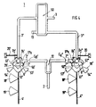
- a second exemplary embodiment, a double modulator stage 1, is shown in FIG. 4. It has the same functional units as the double modulator stage 1 shown in FIG. 3, but is specifically designed for a carrier U c with a frequency in the gigahertz range and for a modulation voltage U m with a frequency in the megahertz range using planar stripline technology.
- the arrangement of the functional units corresponds to that of FIG. 3. Compared to FIG. 3, the same functional units are also provided with the same reference numerals.
- the double modulator stage 1 has two partial modulator stages 1 ', 1 ⁇ with a common carrier input 2 and a common signal output 3.
- the carrier voltage U c is present at the carrier input 2 ', 2 ⁇ of the two partial modulator stages 1', 1 ⁇ via a so-called Wilkinson coupler 12.
- the two carrier inputs 2 ', 2 ⁇ are each electrically isolated from the Wilkinson coupler 12', 12 ⁇ via a capacitance C K1 ', C K1 ⁇ .
- the signal outputs 3 ', 3 ⁇ are brought together via a 180 ° power combiner 50 in the form of a so-called rate race ring.
- the Rate Race Ring 50 has as an input the two signal outputs 3 ', 3 ⁇ of the partial modulator stages 1', 1 ⁇ , as an output the output 3 of the double modulator stage 1 and a 50 ohm termination 13 to ground, it causes another shift of the phases of the from the partial modulator stage 1 'emerging modulated carrier voltage U mc ' compared to the emerging from the partial modulator stage 1 ⁇ carrier voltage U mc ⁇ of 180 ° and thus brings them together in phase.
- the two partial modulator stages 1 ', 1 ⁇ are constructed like the modulator stage 70, the partial modulator stage 1' being mirror-symmetrical with respect to the partial modulator stage 1 ⁇ .
- the second embodiment is constructed in planar stripline technology and equipped with the diodes D1 ', D1 ⁇ , D2', D2 ⁇ .
- FIG. 5 A third embodiment is shown in FIG. 5.
- the double modulator stage 1 shown as for the double modulator stage from FIG. 4, it applies that it has the same functional units as that shown in FIG. 3.
- the same features are therefore provided with the same reference numerals. Specifically, it is designed for a carrier U c with a wavelength in the upper megahertz range and a correspondingly lower frequency of the modulation signal U m .
- the double modulator stage 1 has two partial modulator stages 1 ', 1 ⁇ with a common signal output 3.
- the carrier U c is generated in the oscillator 21, which is on one side to ground 22 and is connected via the other side to the carrier inputs 2 ', 2 ⁇ .
- An autotransformer 23 is located between the oscillator 21 and the carrier inputs 2 'and 2'.
- the oscillator 21 is connected to the tap 24 and the two winding ends 25 'and 25' are via coupling capacitors C K1 'and C K1 ⁇ with the carrier inputs 2 ', 2 ⁇ connected.
- the autotransformer 23 represents a 0 ° power divider and the resistance R21 represents the internal resistance of the oscillator 21.
- the signal outputs 3 ', 3 ⁇ are connected to the two winding ends of the primary winding 26 of a transformer 27, which serves as a transformer 11.
- the winding ends of the secondary winding represent the signal output 3 of the double modulator stage 1.
- high-impedance parallel resonant circuits 29 ', 29' are between the winding ends of the primary coil 26 and the signal outputs 3 'and 3' for the modulation signal U m arranged.
- Each of the two partial modulator stages 1 ', 1 ⁇ has a phase delay path 6', 6 ⁇ and an electrically short path 7 ', 7 ⁇ .
- the phase delay path 6 ', 6 ⁇ has a low pass 60', 60 ⁇ and a semiconductor diode D2 ', D2 ⁇ .
- the low pass 60 ', 60 is made up of discrete components and consists of three series connected inductors 61', 61 ⁇ , 62 ', 62 63, 63', 63 ⁇ and capacitors 64 ', 64 ⁇ between the inductors, 65 ', 65 ⁇ , which are coupled to ground.
- the middle inductance 62 ', 62 ⁇ has a tap 66', 66 ⁇ for feeding in the modulation signal U m ', U m ⁇ .
- the electrically short path 7 ', 7 ⁇ has a semiconductor diode D1' D1 ⁇ . The polarity of the diodes corresponds to that of the other versions.
- the modulation signal is generated in a generator 34 ', 34 ⁇ , which is present at the output 3', 3 ⁇ and via a parallel resonant circuit 35 ', 35 ⁇ with the tap 33 ', 33 ⁇ is connected.
- the resistors R34 ', R34 ⁇ represent the internal resistances of the oscillators 34', 34 ⁇ .
- the parallel resonant circuit 35 ', 35 ⁇ is high-resistance for the carrier U c .
- the low pass 60 ', 60 ⁇ and the two semiconductor diodes D1' D2 '; D1 ⁇ , D2 ⁇ act like a Wheatstone bridge, in which there is equilibrium between the output 3 ', 3 ⁇ and the tap 66', 66 ⁇ as long as there is no modulation voltage U m . However, if there is a modulation voltage U m , the balance of the bridge is removed and the modulated carrier voltage U mc is present at the output 3 ', 3 ⁇ .
- a low-pass filter 39 ', 39 60, 60', 60 ⁇ is of particular importance since it allows many degrees of freedom in the arrangement and design as part of this more complex circuit.
- FIG. 6 known in itself schematic representation of a 16 QAM modulator 49 (Q uadratur A mplituden M odulation) for a bit rate of 140 MBit / s displayed. It essentially consists of two double modulator stages 40, 41, one double modulator stage 40 providing the signal for the I component and the double modulator stage 41 providing the signal for the Q component. The two components are brought together orthogonally in the power combiner 42.
- the output 43 of the power combiner 42 forms the output of the 16 QAM modulator 49.
- the carrier U c is applied to the carrier inputs 2 of the two modulator stages 40, 41 via a so-called Wilkinson coupler 45.
- the modulation signals for the I and Q components are located at the signal inputs 46, 47 of the two double modulator stages 40, 41, a modulation signal U m of the same amount being present at each of the double modulator stages 40, 41 for the I and Q components and opposite signs.
- Schottky diodes are particularly suitable as semiconductor diodes D1 ', D1 ⁇ , D2', D2 ⁇ , which have shorter delay times, for example, compared to pin diodes.
- the temperature dependence of the diodes is compensated for by the arrangement in pairs in the bridge circuit. Production-related differences in the diodes can be compensated for, for example, by applying a DC voltage via the adjustable resistor at the signal input and thus optimizing carrier suppression.
- the controllable resistors R R ', R R ⁇ are each set so that there is no bridge equilibrium in each submodulator stage 1', 1 ⁇ , 70 when the modulation voltage U m is not applied.
- the modulator stage 1 described can also be operated as a transmit or receive mixer stage (not shown).
- the use of modulator stage 1 of the first exemplary embodiment is used as a transmission mixer stage.
- the signal inputs 4 'and 4 ⁇ described in the first embodiment are provided for coupling the frequency to be converted signal.
- the frequency of the signal to be converted must be at one of the two Signal inputs are inverted.
- the two signal inputs can be connected directly to one another.
- the 16 QAM modulator 49 as a mixer, which on the receiving end as Mirror suppressing mixer and can be operated on the transmission side as a single sideband mixer. To do this, however, when utilizing both coupling branches I and Q, it is necessary to connect them to one another via a 90 ° power combiner.
Landscapes
- Physics & Mathematics (AREA)
- Electromagnetism (AREA)
- Engineering & Computer Science (AREA)
- Power Engineering (AREA)
- Digital Transmission Methods That Use Modulated Carrier Waves (AREA)
- Transmitters (AREA)
- Networks Using Active Elements (AREA)
Claims (12)
- Etage modulateur (1) pour la formation d′un signal de porteuse modulé à partir d'une porteuse et d'un signal de modulation, comportant une entrée de porteuse et une entrée de signal (2, 2′, 2˝; 4, 4′, 4˝) et une sortie de signal (3, 3′, 3˝),- selon lequel un chemin électriquement court (7, 7′, 7˝) et un chemin à retard de phase (6, 6′, 6˝) conduisent de l'entrée de porteuse (2, 2′, 2˝) à la sortie de signal (3, 3′, 3˝);- selon lequel la phase de la porteuse subit dans le chemin à retard de phase (6, 6′, 6˝) contrairement à la phase dans le chemin électriquement court (7, 7' 7˝) un déphasage d'environ 180° ou d'un multiple entier impair de 180°;- selon lequel un opérateur à retard de phase est disposé sur le chemin à retard de phase (6, 6′, 6˝);- selon lequel un élément à semi-conducteur non-linéaire (D₁, D₂) se trouve sur chacun des deux chemins (6, 6′, 6˝; 7, 7′, 7˝), lesquels éléments présentent par rapport au sens de propagation de la porteuse, une polarité inversée et sont disposés sur les deux chemins de façon telle qu'ils puissent fonctionner en mode commun par rapport à la porteuse.
- Etage modulateur selon la revendication 1, caractérisé en ce que le passe-bas (39) comporte un nombre impair d'éléments et en ce qu'une inductance (50, 52) est disposée à chaque extrémité du chemin à retard de phase (6).
- Etage modulateur selon la revendication 2, caractérisé en ce que le passe-bas (39) comporte trois inductances (50, 51, 52) montées en série, entre lesquelles une capacité (53, 54) mise à la masse est chaque fois disposée.
- Etage modulateur selon l'une des revendications 1 à 3, caractérisé en ce que la fréquence limite (fG) du passe-bas (39) correspond sensiblement au deuxième harmonique de la fréquence porteuse (fc).
- Etage modulateur selon l'une des revendications précitées 1 à 4, caractérisé en ce qu'il est prévu comme circuit intégré monolithique à micro-ondes (MMIC).
- Etage modulateur selon l'une des revendications précitées 1 à 4, caractérisé en ce qu'il est connu au moins principalement comme une structure planaire à microbandes.
- Etage modulateur selon l'une des revendications précitées 1 à 6, caractérisé- en ce que l'étage modulateur est conçu sous forme d'étage modulateur double (1) comportant deux étages modulateurs partiels (1′, 1˝),- en ce que les deux entrées de porteuse (2′, 2˝) et les deux sorties de signal (3′, 3˝) des deux étages modulateurs partiels (1′, 1˝) sont reliées entre elles,- en ce que les mêmes signaux de valeur identique mais à signe inverse sont placés sur les entrées de signal (4′, 4˝), et- en ce qu'un dispositif (11, 23) est prévu pour l'addition scalaire de la tension de porteuse (Umc′, Umc˝) modulée et déphasée de 180° des étages modulateurs partiels 1′ et 1˝.
- Etage modulateur selon la revendication 7, caractérisé en que le dispositif (11) pour l'addition scalaire est un coupleur de 180° (11) qui est disposé entre les sorties (3′, 3˝) des étages modulateurs partiels (1′, 1˝) et la sortie (3) de l'étage modulateur double (1).
- Etage modulateur selon la revendication 1, caractérisé en ce que chaque entrée de signal (4, 4′, 4˝) des étages modulateurs (39, 1′, 1˝) est pourvue d'une résistance réglable (RR′, RR˝) pour l'équilibrage de l'étage modulateur.
- Etage modulateur selon la revendication 1, caractérisé en ce que l'élément à semi-conducteur non linéaire (D₁, D₂, D₁′, D₂′, D₁˝, D₂˝) est une diode de Schottky.
- Etage modulateur selon la revendication 1, caractérisé en ce que les étages modulateurs (39, 1′, 1˝) se présentent sous forme d'inverseurs de phase linéaires en amplitude.
- Etage modulateur selon l'une des revendications précédentes 1 à 11, caractérisé en ce qu'il est utilisé comme étage mélangeur.
Applications Claiming Priority (2)
| Application Number | Priority Date | Filing Date | Title |
|---|---|---|---|
| DE4028371 | 1990-09-07 | ||
| DE4028371A DE4028371A1 (de) | 1990-09-07 | 1990-09-07 | Modulator- und mischstufe |
Publications (2)
| Publication Number | Publication Date |
|---|---|
| EP0480145A1 EP0480145A1 (fr) | 1992-04-15 |
| EP0480145B1 true EP0480145B1 (fr) | 1995-06-14 |
Family
ID=6413769
Family Applications (1)
| Application Number | Title | Priority Date | Filing Date |
|---|---|---|---|
| EP91113801A Expired - Lifetime EP0480145B1 (fr) | 1990-09-07 | 1991-08-17 | Etage modulateur et mélangeur |
Country Status (6)
| Country | Link |
|---|---|
| US (1) | US5214397A (fr) |
| EP (1) | EP0480145B1 (fr) |
| JP (1) | JP3188734B2 (fr) |
| CA (1) | CA2050756C (fr) |
| DE (2) | DE4028371A1 (fr) |
| ES (1) | ES2076431T4 (fr) |
Families Citing this family (5)
| Publication number | Priority date | Publication date | Assignee | Title |
|---|---|---|---|---|
| DE4028370A1 (de) * | 1989-12-14 | 1991-06-20 | Standard Elektrik Lorenz Ag | Modulator- und mischstufe |
| FI90165C (fi) * | 1991-12-13 | 1993-12-27 | Nokia Mobile Phones Ltd | I/q-modulator och demodulator |
| GB2281830B (en) * | 1993-09-11 | 1998-08-12 | Nokia Mobile Phones Ltd | I/q-modulator and i/q-demodulator |
| GB2282287B (en) * | 1993-09-25 | 1998-01-28 | Nokia Mobile Phones Ltd | A mixer |
| US6759742B2 (en) * | 1999-10-12 | 2004-07-06 | The Whitaker Corporation | Interchangeable bond-wire interconnects |
Family Cites Families (5)
| Publication number | Priority date | Publication date | Assignee | Title |
|---|---|---|---|---|
| JPS5563106A (en) * | 1978-11-06 | 1980-05-13 | Hitachi Ltd | Mixer circuit |
| DE3117080A1 (de) * | 1981-04-29 | 1982-11-18 | Siemens AG, 1000 Berlin und 8000 München | Mikrowellen-gegentaktmischerschaltung in streifenleitungstechnik |
| US4528526A (en) * | 1983-05-31 | 1985-07-09 | Motorola, Inc. | PSK modulator with noncollapsable output for use with a PLL power amplifier |
| US4607394A (en) * | 1985-03-04 | 1986-08-19 | General Electric Company | Single balanced planar mixer |
| US4612518A (en) * | 1985-05-28 | 1986-09-16 | At&T Bell Laboratories | QPSK modulator or demodulator using subharmonic pump carrier signals |
-
1990
- 1990-09-07 DE DE4028371A patent/DE4028371A1/de not_active Withdrawn
-
1991
- 1991-08-17 EP EP91113801A patent/EP0480145B1/fr not_active Expired - Lifetime
- 1991-08-17 ES ES91113801T patent/ES2076431T4/es not_active Expired - Lifetime
- 1991-08-17 DE DE59105701T patent/DE59105701D1/de not_active Expired - Fee Related
- 1991-09-05 CA CA002050756A patent/CA2050756C/fr not_active Expired - Fee Related
- 1991-09-06 JP JP25457791A patent/JP3188734B2/ja not_active Expired - Fee Related
- 1991-09-06 US US07/756,183 patent/US5214397A/en not_active Expired - Fee Related
Non-Patent Citations (1)
| Title |
|---|
| Mai 1982 & JP-A-57 011 506 ( HITACHI SEISAKUSHO K.K. ) 21. Januar 1982 * |
Also Published As
| Publication number | Publication date |
|---|---|
| EP0480145A1 (fr) | 1992-04-15 |
| DE59105701D1 (de) | 1995-07-20 |
| ES2076431T3 (es) | 1995-11-01 |
| JPH04257147A (ja) | 1992-09-11 |
| JP3188734B2 (ja) | 2001-07-16 |
| CA2050756A1 (fr) | 1992-03-08 |
| DE4028371A1 (de) | 1992-03-12 |
| ES2076431T4 (es) | 1997-01-16 |
| CA2050756C (fr) | 1994-05-03 |
| US5214397A (en) | 1993-05-25 |
Similar Documents
| Publication | Publication Date | Title |
|---|---|---|
| DE4420377C2 (de) | Verfahren zum Erzeugen von Quadratursignalen | |
| DE69623292T2 (de) | Bipolarer analogmultiplizierer für niederspannungsanwendungen | |
| DE102006017189B4 (de) | Integrierte Oszillatorschaltung mit wenigstens zwei Schwingkreisen | |
| DE3916406C2 (de) | Doppelt-symmetrischer Mischer | |
| EP0432674B1 (fr) | Modulateur d'amplitude en quadrature à suppression améliorée de la porteuse | |
| DE69609998T2 (de) | Symmetrische Phasenteilerschaltung | |
| EP0360916A1 (fr) | Atténuateur à micro-ondes monolithique en circuit intégré | |
| DE10344876B3 (de) | Signalverarbeitungseinrichtung, insbesondere für den Mobilfunk | |
| EP0480145A1 (fr) | Etage modulateur et mélangeur | |
| EP0728391B1 (fr) | Circuit d'extraction de signal d'horloge | |
| DE60101089T2 (de) | Multifunktionelle integrierte schaltungsanordnung hoher frequenz | |
| DE3246295C2 (de) | Frequenzmodulierbarer Oszillator | |
| EP0614273B1 (fr) | Circuit de filtrage comportant un résonateur fonctionnant comme circuit résonant en série | |
| DE3324540C2 (de) | Breitbandiger Mikrowellenverstärker | |
| EP0133618A1 (fr) | Circuit oscillateur haute fréquence à quartz sous forme de circuit intégré monolithique | |
| DE2646035C3 (de) | Wechselspannungsschaltung mit mehreren in Basis-(Gate-) Schaltung betriebenen Halbleiterverstärkerelementen | |
| EP0142182A2 (fr) | Montage pour la conversion d'un signal d'entrée numérique en un signal de sortie analogique | |
| DE19754114C2 (de) | Mischvorrichtung zum Mischen eines ersten und eines zweiten Signals mit gegenseitig verschiedenen Frequenzen | |
| DE102012208529A1 (de) | Elektronischer Schalter mit Kompensation nichtlinearer Verzerrungen | |
| DE69907324T2 (de) | Oszillator mit zwei Quadraturausgängen | |
| EP0687062A1 (fr) | Déphaseur analogue pour petites tensions de commande | |
| DE2436647A1 (de) | Antennensystem fuer eine hf-einrichtung zur erzeugung verschiedener antennencharakteristiken | |
| DE1952135B1 (de) | Nichtreziproke Reaktanzverstaerkeranordnung | |
| EP1509996B1 (fr) | Convertisseur de frequence vers le haut | |
| DE102004002826B4 (de) | Schaltung zur Änderung einer Frequenz |
Legal Events
| Date | Code | Title | Description |
|---|---|---|---|
| PUAI | Public reference made under article 153(3) epc to a published international application that has entered the european phase |
Free format text: ORIGINAL CODE: 0009012 |
|
| AK | Designated contracting states |
Kind code of ref document: A1 Designated state(s): DE ES FR GB IT NL SE |
|
| 17P | Request for examination filed |
Effective date: 19920819 |
|
| RAP3 | Party data changed (applicant data changed or rights of an application transferred) |
Owner name: ALCATEL N.V. Owner name: ALCATEL SEL AKTIENGESELLSCHAFT |
|
| 17Q | First examination report despatched |
Effective date: 19940425 |
|
| GRAA | (expected) grant |
Free format text: ORIGINAL CODE: 0009210 |
|
| AK | Designated contracting states |
Kind code of ref document: B1 Designated state(s): DE ES FR GB IT NL SE |
|
| ITF | It: translation for a ep patent filed | ||
| REF | Corresponds to: |
Ref document number: 59105701 Country of ref document: DE Date of ref document: 19950720 |
|
| GBT | Gb: translation of ep patent filed (gb section 77(6)(a)/1977) |
Effective date: 19950703 |
|
| ET | Fr: translation filed | ||
| REG | Reference to a national code |
Ref country code: ES Ref legal event code: FG2A Ref document number: 2076431 Country of ref document: ES Kind code of ref document: T4 |
|
| PLBE | No opposition filed within time limit |
Free format text: ORIGINAL CODE: 0009261 |
|
| STAA | Information on the status of an ep patent application or granted ep patent |
Free format text: STATUS: NO OPPOSITION FILED WITHIN TIME LIMIT |
|
| 26N | No opposition filed | ||
| PGFP | Annual fee paid to national office [announced via postgrant information from national office to epo] |
Ref country code: NL Payment date: 19990719 Year of fee payment: 9 |
|
| PG25 | Lapsed in a contracting state [announced via postgrant information from national office to epo] |
Ref country code: NL Free format text: LAPSE BECAUSE OF NON-PAYMENT OF DUE FEES Effective date: 20010301 |
|
| NLV4 | Nl: lapsed or anulled due to non-payment of the annual fee |
Effective date: 20010301 |
|
| PGFP | Annual fee paid to national office [announced via postgrant information from national office to epo] |
Ref country code: SE Payment date: 20010802 Year of fee payment: 11 |
|
| PGFP | Annual fee paid to national office [announced via postgrant information from national office to epo] |
Ref country code: ES Payment date: 20010803 Year of fee payment: 11 |
|
| REG | Reference to a national code |
Ref country code: GB Ref legal event code: IF02 |
|
| PG25 | Lapsed in a contracting state [announced via postgrant information from national office to epo] |
Ref country code: SE Free format text: LAPSE BECAUSE OF NON-PAYMENT OF DUE FEES Effective date: 20020818 Ref country code: ES Free format text: LAPSE BECAUSE OF NON-PAYMENT OF DUE FEES Effective date: 20020818 |
|
| EUG | Se: european patent has lapsed | ||
| PGFP | Annual fee paid to national office [announced via postgrant information from national office to epo] |
Ref country code: GB Payment date: 20030728 Year of fee payment: 13 |
|
| PGFP | Annual fee paid to national office [announced via postgrant information from national office to epo] |
Ref country code: DE Payment date: 20030805 Year of fee payment: 13 |
|
| PGFP | Annual fee paid to national office [announced via postgrant information from national office to epo] |
Ref country code: FR Payment date: 20030813 Year of fee payment: 13 |
|
| REG | Reference to a national code |
Ref country code: ES Ref legal event code: FD2A Effective date: 20030912 |
|
| PG25 | Lapsed in a contracting state [announced via postgrant information from national office to epo] |
Ref country code: GB Free format text: LAPSE BECAUSE OF NON-PAYMENT OF DUE FEES Effective date: 20040817 |
|
| PG25 | Lapsed in a contracting state [announced via postgrant information from national office to epo] |
Ref country code: DE Free format text: LAPSE BECAUSE OF NON-PAYMENT OF DUE FEES Effective date: 20050301 |
|
| GBPC | Gb: european patent ceased through non-payment of renewal fee |
Effective date: 20040817 |
|
| PG25 | Lapsed in a contracting state [announced via postgrant information from national office to epo] |
Ref country code: FR Free format text: LAPSE BECAUSE OF NON-PAYMENT OF DUE FEES Effective date: 20050429 |
|
| REG | Reference to a national code |
Ref country code: FR Ref legal event code: ST |
|
| PG25 | Lapsed in a contracting state [announced via postgrant information from national office to epo] |
Ref country code: IT Free format text: LAPSE BECAUSE OF NON-PAYMENT OF DUE FEES;WARNING: LAPSES OF ITALIAN PATENTS WITH EFFECTIVE DATE BEFORE 2007 MAY HAVE OCCURRED AT ANY TIME BEFORE 2007. THE CORRECT EFFECTIVE DATE MAY BE DIFFERENT FROM THE ONE RECORDED. Effective date: 20050817 |