EP0480165A2 - Digitale Taktgewinnungsschaltung vom Integratortyp - Google Patents
Digitale Taktgewinnungsschaltung vom Integratortyp Download PDFInfo
- Publication number
- EP0480165A2 EP0480165A2 EP91114698A EP91114698A EP0480165A2 EP 0480165 A2 EP0480165 A2 EP 0480165A2 EP 91114698 A EP91114698 A EP 91114698A EP 91114698 A EP91114698 A EP 91114698A EP 0480165 A2 EP0480165 A2 EP 0480165A2
- Authority
- EP
- European Patent Office
- Prior art keywords
- data
- retiming
- data edge
- retiming signal
- signal
- Prior art date
- Legal status (The legal status is an assumption and is not a legal conclusion. Google has not performed a legal analysis and makes no representation as to the accuracy of the status listed.)
- Withdrawn
Links
Images


Classifications
-
- H—ELECTRICITY
- H04—ELECTRIC COMMUNICATION TECHNIQUE
- H04L—TRANSMISSION OF DIGITAL INFORMATION, e.g. TELEGRAPHIC COMMUNICATION
- H04L7/00—Arrangements for synchronising receiver with transmitter
- H04L7/02—Speed or phase control by the received code signals, the signals containing no special synchronisation information
- H04L7/033—Speed or phase control by the received code signals, the signals containing no special synchronisation information using the transitions of the received signal to control the phase of the synchronising-signal-generating means, e.g. using a phase-locked loop
- H04L7/0337—Selecting between two or more discretely delayed clocks or selecting between two or more discretely delayed received code signals
- H04L7/0338—Selecting between two or more discretely delayed clocks or selecting between two or more discretely delayed received code signals the correction of the phase error being performed by a feed forward loop
Definitions
- This invention relates in general to communication systems and information and data processing systems, and more particularly, to digital phase locked logic circuits for extracting a retiming signal from a received serial data stream.
- PLLs Phase locked loops
- PLLs are a critical component in many data communication networks. PLLs are used for locally maintaining in remote stations a clock signal that corresponds in frequency and phase to the clock of data signals transmitted through the network and received by the station. The difference between a VCO generated signal and the clock signal recovered from the received data is monitored and the phase and frequency of the VCO signal is adapted and "locked" to that of the received data signal.
- the evaluation means which instantaneously corrects the output clock signal on every data edge transition, typically includes an encoder and a look-up table. Although somewhat successful under jitter conditions, the technique experiences difficulty in differentiating between noise and valid data transitions, especially in a high jitter environment.
- the DPLL clock extractor as claimed is designed to address and expand upon the performance limitations of existing digital data retiming circuit technology, and in particular, to allow for higher accuracy in data retiming under high jitter and/or high noise conditions.
- this invention comprises in one aspect a method for selecting a retiming signal for a received serial data stream from a plurality of local clock signals of different phase.
- the method includes the steps of: sorting in time M data edge transitions of the serial stream; and selecting a retiming signal from the plurality of local clock signals which coincides in time with a minimum number of the M sorted data edge transitions.
- subsequent selection of the initial retiming signal includes: sorting in time N additional data edge transitions of the serial stream; and selecting a new retiming signal from the plurality of local clock signals such that the new retiming signal coincides in time with a minimum number of the N (or M + N) sorted data edge transitions. Additional method features are also described and claimed herein.
- the invention comprises apparatus for selecting a retiming signal for a serial data stream.
- a data edge sorting circuit which is coupled to receive the serial data stream, operates to phase sort a plurality of data edge transitions of the serial stream.
- Generating means is provided for producing a plurality of local clock signals of different phase from which a retiming signal is selected.
- Integrating means is coupled to the data edge sorting circuit to receive the sorted data edge transitions and comparison means is coupled to the integrating means for identifying a proper retiming clock phase from the plurality of generated local clock signals by comparison thereof with the integrated data edge transitions.
- the comparison means comprises clock selection logic
- the integration means includes time slot counters
- the relative time slot counter values are output to the clock selection logic for identification of a compatible retiming clock phase.
- the present inventive technique features the creation of a histogram of a preselected number of data edge transitions and use thereof to select an appropriate data retiming signal from a plurality of locally available DPLL clock signals.
- the histogram is re-examined after every N data edge sorts and a new data edge retiming signal is chosen based thereon.
- the integrated approach described herein allows accurate data retiming even of highly jittered and/or noisy data streams.
- the technique is suitable for high speed applications and can be realized in hardware or in hardware/software combinations.
- the present invention comprises a control technique for selecting an appropriate clock signal, from a plurality of locally generated clock signals of different phase, for use in retiming of a serial data stream.
- the technique is based on the integration and periodic analysis of a plurality of sorted data edge transitions.
- a retiming clock selection is preferably re-evaluated after every N data edge transition sorts.
- the resultant data edge histogram can be cumulative of all sorted transitions or merely cumulative of the last N sorted transitions.
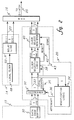
- Retiming circuit 10 includes a digital phase locked logic circuit (DPLL) 12, a clock phase generator 14, a multiplexer 16 and an edge triggered D-latch 18.
- DPLL digital phase locked logic circuit
- DPLLs are now well known in the art and will therefore not be described in detail herein.
- a serial stream of clock and data signals to be retimed, and subsequently deserialized is received on line 13 which is coupled to an input of a DPLL front end circuit 15.
- DPLL front end circuit 15 results from a somewhat arbitrary division of DPLL 12. Circuit 15 receives from generator 14 on lines 17 a plurality of clock signals of different phase.
- Generator 14 and circuit 15 components may include, for example, a local clock generator, a clock delay line and data edge sorting circuitry. Such components are described in the referenced U.S. Patent No. 4,677,648, the entirely of which is hereby incorporated herein by reference.
- DPLL front end circuit 15 through its data edge sorting circuitry (see Figure 2), outputs a plurality of pulse signals C(1), C(2)...C(S-1) & C(S) on an equivalent number of lines 19, which are coupled to a choose correct clock circuit 20.
- Circuits 15 & 20 essentially comprise digital phase lock logic circuit 12, shown in phantom in Figure 1.
- the S outputs C(1), C(2)... C(S-1) & C(S) from circuit 15 represent discrete time intervals relative to the DPLL local clock. The leading edge of one time interval occurs precisely at the trailing edge of the previous interval.
- a pulse signal for each data edge transition of the serial stream is provided on a corresponding one of the S outputs to signify the location in time of the transition relative to the DPLL local clock.
- Choose correct clock circuit 20 operates to select a proper local clock phase for use in data retiming from a plurality of local clocks of identical frequency but different phase.
- the present invention is specifically directed to this DPLL function. Again, pursuant to the invention, clock selection is made based upon an analysis of the historical distribution of a predefined number of sorted data edge transitions.
- An identification of a selected clock signal is output from DPLL 12 on line 21 to a multiplexer 16 which also receives as input (on line 23) a plurality of local clock signals of different phase produced by clock phase generator 14.
- the output (on line 25) of multiplexer 16 is fed to the clock input "C" of edge triggered data latch 18.
- a second, data input "D" to latch 18 is coupled to line 13 for receiving the serial data stream. Data is latched on either the rising or falling clock edge.
- Retimed data is output from latch 18 on line 27, for example, to a deserialization circuit (not shown).
- a data edge sorting circuit 30 in DPLL front end circuit 15 provides circuit 20 with an instantaneous indication of the approximate location in time of a data edge transition relative to the DPLL local clock produced by generator 14. Successive location indications are transmitted from circuit 30 via S lines 19 to a corresponding number of time slot counters 32 located in circuit 20.
- the local reference clock produced by generator 14 and used by DPLL circuit 12 is configured to cover one period or more of the input data clock. This guarantees that each data edge transition will be detected and sorted into one of the S time intervals or slots.
- two time slot counters will initially (and thereafter periodically) accumulate counts at a faster rate than the remaining counters, even under a high jitter or high noise condition. This information can be beneficially used to select an appropriate clock signal phase.
- Counters 32 thus integrate (accumulate a historical overview of) the locations of successive sorted data edge transitions.
- the present technique employs this histogram to initially select and then re-select a proper retiming clock phase.
- a preferred retiming signal will occur at a flat or null in the histogram, i.e., at a time interval containing a relative "minimum number" (herein defined to be zero or a nonzero minimum number) of sorted data edge transition representations.
- minimum number herein defined to be zero or a nonzero minimum number
- data edge sorting circuit 30 may signal a constantly changing timing of data edge transitions relative to the local clock.
- the data edge transition locations will slowly roll through the time slot counters, which produces a slowly shifting histogram.
- lines 19 are mutually exclusive in that only one is active in any given data cycle. The active line indicates the location in time of a present data edge transition relative to the local DPLL clock.
- Counters block 32 also includes a total counter which outputs a signal on line 35 to a clock selection logic 38.
- the total counter functions to provide logic 38 with an indication of when a prechosen number (M or N, discussed below) of data transitions have occurred, i.e., have been counted by the time slot counters.
- the outputs 33 of the time slot counters are coupled to logic 38 and to a modification logic 34.
- Logic 34 which outputs to the time slot counters an attenuate signal on line 36, operates to prevent overflow of the time slot counters and therefore loss of information, and in a preferred embodiment described below, to provide better continuity between data sort samples. This logic maintains the time slot counters at a reasonable level relative to their capacity. For example, logic 34 typically operates to proportionately reduce, e.g. by some constant value, each time slot counter should the value of any one counter exceed a predefined threshold. Modification logic 34 includes appropriate comparative circuitry to accomplish this function.
- clock selection logic 38 which is broadly used herein to include any circuit components, such as registers, necessary to accomplish the functions described below.
- Clock selection logic 38 has two primary functions. First, the circuit confirms that the histogram stored in time slot counters 32 meets certain predefined specification requirements for selection of a retiming clock and, second, the circuit decides on an appropriate retiming clock phase from the plurality of available local DPLL signals of different phase.
- clock selection logic 38 can be replaced by a processor, and counters 32 by a set of registers readable by the processor. This alternate embodiment is preferred for low frequency operation, e.g. less than 20 MHz., but for higher frequency operation the clock selection logic is preferred.
- Logic 38 outputs on lines 41 a clock address indication K bits in length which comprises an identification of a selected retiming clock signal.
- This address identifier is sent to a clock select register 40 where the signal is latched on lines 21 to a multiplexer 16, which multiplexes the address with 1 through K local clocks of the same frequency but different phase produced by generator 14, for example, through a delay line 50 supplied by local clock 48.
- the output of multiplexer 16 is connected to the clock input "C" of D-latch 18 ( Figure 1) via line 25.
- Clock selection logic 38 also outputs to a reset line 42 coupled to register 40 for resetting the register, for example, should the input signal become lost.
- a reset line 42 coupled to register 40 for resetting the register, for example, should the input signal become lost.
- the store signal on line 43 which is also coupled to register 40, directs the register to begin latching information from logic 38, thereby simultaneously result in outputting of the retiming clock.
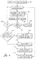
- a preferred processing technique for clock selection logic 38 utilizes two fundamental modes: an acquiring mode ( Figure 3) and a tracking mode ( Figure 4). Each of these modes will now be described.
- processing is begun, 60 "Start,” by clearing the S time slot counters and the total counter, 62 “Reset Time Slot Counters and Total Counter.” Thereafter, the time slot counters are incremented with each sorted data edge transition, 64 "Increment Time Slot Counters With n-th Data Edge Sort,” along with the total counter, 66 “Increment Total Counter.” After a sorted transition is stored in the appropriate counter, inquiry is made as to whether any counter has reached a predefined upper limit, 68 "Is Any Counter Full?" If "yes”, all counters are attenuated, e.g., by a predefined constant, so as to maintain the same ratios therebetween. Thereafter, processing is continued and the next sorted data edge is stored in the appropriate time slot counter.
- the predefined specification requirements are needed to insure that the compiled data edge transition history is truly indicative of a coherent data stream.
- specification requirements might be that (1) at least one counter has a count greater than 10 data edge sorts; and (2) at least one counter has a count less than or equal to one data edge sort.
- the specification requirements are selected to ensure that there exists some significant ratio between the time slot counts, i.e., that a relative minimum or a null in the time slot counts is identifiable.
- a principal object hereof is to select a retiming signal which coincides with a minimum number of accumulated data edge transitions and, thus, to select a signal which least interferes with future data edge transitions.
- an initial data retiming clock phase is selected, 76 "Select Best Initial Data Retiming Clock.”
- the clock is selected from the plurality of local DPLL clocks of different phase generated, for example, by delay line 50 ( Figure 2).
- Figure 2 Various mathematical techniques exist for dealing with a grouped sample statistic which can be used to identify the best retiming clock phase. For example, see W. Cramer, Mathematical Methods of Statistics , published by the University of Swedish, 1946, and references cited therein. Again the object is to select a time slot where a relative minimum number of the M integrated data edge transitions have occurred.
- At least one time slot counter should be below a predefined lower threshold count level to ensure that the selected retiming clock will not interfere with future data transitions of the received signal.
- One technique for selecting a clock signal is to split the difference between the two closest time slot counters with counts above a preselected upper threshold. Alternatively, if only one time slot counter is above the upper threshold, then one-half a local clock cycle could be added to the one counter to identify a preferred retiming clock phase. In practice, the resultant histogram should also be evaluated to detect any unexpected count build ups of the time slot counter values.
- An address identifying the selected retiming clock is next stored in the clock select register 40, 78 "Store Selected Data Retiming Clock I.D.,” and data retiming is begun with the selected clock, 80 "Start Data Retiming With Initial Clock,” after which, the system proceeds to the second mode, or normal mode, 82 "Go To Tracking Mode.”
- sample size N used in the tracking mode may be smaller than sample size M of the acquiring mode.
- M In the acquiring mode, M must be sufficiently large so that the distribution of data edge transitions provides a sufficient sampling basis to select an initial retiming clock.
- the sample size N is selected based upon the maximum frequency difference between the local DPLL clock and the input stream clock. (Preferably, the N tracking mode data sorts are added to the M acquiring mode sorts, rather than beginning a new history with each new sample interval.)
- a large frequency difference between the DPLL clock and the input clock implies a constantly changing phase and therefore a constantly changing retiming clock signal is needed. Again, except for the sample size, the operation is substantially the same as in the acquiring mode.
- sample size M of the acquiring mode is defined to be relatively small to allow quick locking to an acceptable clock phase and sample size N of the tracking mode is defined to be relatively large (assuming that the local clock frequency is close to the data signal frequency) to desensitize the clock selection operations from input jitter.
- the retimed data is inhibited and a new attempt at acquisition is initiated, 106 "Stop Data Retiming and Go To Acquiring Mode.” If the sample distribution is acceptable, the best data retiming clock is again selected, 108 "Select Best Data Retiming Clock,” stored, 110 "Store Selected Retiming Clock I.D.,” and data retiming is begun using the new clock, 112 "Start Data Retiming With New Clock.” In tracking mode, the entire process is repeated for each set of N data edge transitions. As noted, the time slot counters may be reset at the beginning of each group of N sorts or remain as compiled to provide continuity between groups.
- the present invention contains the features initially set forth herein.
- the described method and apparatus each require a histogram of a prechosen number of data edge transitions for analysis and comparison thereof with a plurality of generated local clocks of different phase.
- a retiming signal is selected to coincide with a relative minimum number of past transitions, thereby optimizing retiming of received data.
- the histogram is re-examined after every N data edge sorts and a new retiming signal is chosen based thereon.
- the technique allows accurate data retiming even for a highly jittered and/or noisy data stream and is suitable for high speed applications.
- the method and apparatus can be realized in hardware or in hardware/software combinations.
Landscapes
- Engineering & Computer Science (AREA)
- Computer Networks & Wireless Communication (AREA)
- Signal Processing (AREA)
- Synchronisation In Digital Transmission Systems (AREA)
Applications Claiming Priority (2)
| Application Number | Priority Date | Filing Date | Title |
|---|---|---|---|
| US07/594,242 US5185768A (en) | 1990-10-09 | 1990-10-09 | Digital integrating clock extractor |
| US594242 | 1990-10-09 |
Publications (2)
| Publication Number | Publication Date |
|---|---|
| EP0480165A2 true EP0480165A2 (de) | 1992-04-15 |
| EP0480165A3 EP0480165A3 (en) | 1993-06-16 |
Family
ID=24378112
Family Applications (1)
| Application Number | Title | Priority Date | Filing Date |
|---|---|---|---|
| EP19910114698 Withdrawn EP0480165A3 (en) | 1990-10-09 | 1991-08-31 | Digital integrating clock extractor |
Country Status (3)
| Country | Link |
|---|---|
| US (1) | US5185768A (de) |
| EP (1) | EP0480165A3 (de) |
| JP (1) | JPH0795732B2 (de) |
Cited By (4)
| Publication number | Priority date | Publication date | Assignee | Title |
|---|---|---|---|---|
| WO1998033292A1 (en) * | 1997-01-23 | 1998-07-30 | Ericsson Inc. | Digital phase aquisition with delay-locked loop |
| US6456677B1 (en) | 1996-06-04 | 2002-09-24 | Matsushita Electric Industrial Co., Ltd. | Synchronization equipment |
| EP1351429A1 (de) * | 2002-03-27 | 2003-10-08 | Kabushiki Kaisha Toshiba | Taktrückgewinnungsschaltung |
| WO2004105303A1 (en) | 2003-04-29 | 2004-12-02 | Telefonaktiebolaget Lm Ericsson (Publ) | Multiphase clock recovery |
Families Citing this family (18)
| Publication number | Priority date | Publication date | Assignee | Title |
|---|---|---|---|---|
| JPH0778774B2 (ja) * | 1991-02-22 | 1995-08-23 | インターナショナル・ビジネス・マシーンズ・コーポレイション | 短待ち時間データ回復装置及びメッセージデータの同期化方法 |
| WO1995001021A1 (en) * | 1993-06-25 | 1995-01-05 | Xircom, Incorporated | Nrz clock recovery with instant lock |
| KR970002949B1 (ko) * | 1994-05-25 | 1997-03-13 | 삼성전자 주식회사 | 디지탈 통신시스템의 클럭발생방법 및 그 회로 |
| US5654988A (en) * | 1995-09-29 | 1997-08-05 | Intel Corporation | Apparatus for generating a pulse clock signal for a multiple-stage synchronizer |
| US5761254A (en) * | 1996-01-31 | 1998-06-02 | Advanced Micro Devices, Inc. | Digital architecture for recovering NRZ/NRZI data |
| JP2806863B2 (ja) * | 1996-02-27 | 1998-09-30 | 日本電気エンジニアリング株式会社 | ビット同期回路 |
| US6570916B1 (en) | 1997-03-04 | 2003-05-27 | Semiconductor Components Industries Llc | Adaptive equalization circuit and method |
| US5910742A (en) * | 1997-06-16 | 1999-06-08 | Cypress Semiconductor Corp. | Circuit and method for data recovery |
| US6181757B1 (en) * | 1998-04-27 | 2001-01-30 | Motorola Inc. | Retiming method and means |
| US6359479B1 (en) * | 1998-08-04 | 2002-03-19 | Juniper Networks, Inc. | Synchronizing data transfers between two distinct clock domains |
| US6366307B1 (en) * | 2000-03-24 | 2002-04-02 | Hewlett-Packard Co. | Clock independent pulse width modulation |
| US6593791B1 (en) * | 2002-04-03 | 2003-07-15 | Applied Micro Circuits Corporation | Precision digital delay element having stable operation over varied manufacturing processes and environmental operating conditions |
| US6597213B1 (en) * | 2002-04-03 | 2003-07-22 | Applied Micro Circuits Corporation | Cascadable frequency doubler having stable operation over varied manufacturing processes and environmental operating conditions |
| US20050013396A1 (en) * | 2003-07-15 | 2005-01-20 | Adtran, Inc. | Digital clock recovery circuit employing fixed clock oscillator driving fractional delay line |
| US7397876B2 (en) * | 2004-08-11 | 2008-07-08 | International Business Machines Corporation | Methods and arrangements for link power reduction |
| US7856283B2 (en) * | 2005-12-13 | 2010-12-21 | Sigmatel, Inc. | Digital microphone interface, audio codec and methods for use therewith |
| US9128643B2 (en) * | 2012-05-17 | 2015-09-08 | Silicon Motion Inc. | Method and apparatus performing clock extraction utilizing edge analysis upon a training sequence equalization pattern |
| US9112655B1 (en) * | 2013-07-30 | 2015-08-18 | Altera Corporation | Clock data recovery circuitry with programmable clock phase selection |
Family Cites Families (20)
| Publication number | Priority date | Publication date | Assignee | Title |
|---|---|---|---|---|
| US3504340A (en) * | 1967-05-08 | 1970-03-31 | Ibm | Triple error correction circuit |
| US3986126A (en) * | 1975-05-15 | 1976-10-12 | International Business Machines Corporation | Serial pulse-code-modulated retiming system |
| US4305045A (en) * | 1979-11-14 | 1981-12-08 | Bell Telephone Laboratories, Incorporated | Phase locked loop clock synchronizing circuit with programmable controller |
| JPS6074745A (ja) * | 1983-09-30 | 1985-04-27 | Hitachi Ltd | タイミング抽出回路 |
| US4584695A (en) * | 1983-11-09 | 1986-04-22 | National Semiconductor Corporation | Digital PLL decoder |
| US4672639A (en) * | 1984-05-24 | 1987-06-09 | Kabushiki Kaisha Toshiba | Sampling clock pulse generator |
| EP0185779B1 (de) * | 1984-12-21 | 1990-02-28 | International Business Machines Corporation | Digitale Phasenregelschleife |
| US4653074A (en) * | 1985-01-24 | 1987-03-24 | Sperry Corporation | Bit sync generator |
| IT1200896B (it) * | 1985-12-18 | 1989-01-27 | Sgs Microelettronica Spa | Circuito di risincronizzazione di segnali impulsivi,particolarmente per periferiche di microprocessori |
| US4841551A (en) * | 1987-01-05 | 1989-06-20 | Grumman Aerospace Corporation | High speed data-clock synchronization processor |
| US5022057A (en) * | 1988-03-11 | 1991-06-04 | Hitachi, Ltd. | Bit synchronization circuit |
| US4819251A (en) * | 1988-05-06 | 1989-04-04 | Rockwell International Corporation | High speed non-return-to-zero digital clock recovery apparatus |
| US4972444A (en) * | 1988-07-14 | 1990-11-20 | International Business Machines Corporation | Digital phase-locked device and method |
| US5034967A (en) * | 1988-11-14 | 1991-07-23 | Datapoint Corporation | Metastable-free digital synchronizer with low phase error |
| US5095498A (en) * | 1989-02-06 | 1992-03-10 | Motorola, Inc. | Bit synchronizer |
| US4908842A (en) * | 1989-02-14 | 1990-03-13 | Galen Collins | Flash synchronized gated sample clock generator |
| ATE110505T1 (de) * | 1989-02-23 | 1994-09-15 | Siemens Ag | Verfahren und anordnung zum anpassen eines taktes an ein plesiochrones datensignal und zu dessen abtakten mit dem angepassten takt. |
| US4959846A (en) * | 1989-09-11 | 1990-09-25 | Raynet Corporation | Clock recovery apparatus including a clock frequency adjuster |
| US5022056A (en) * | 1989-10-23 | 1991-06-04 | National Semiconductor Corporation | Method and structure for digital phase synchronization |
| US5036528A (en) * | 1990-01-29 | 1991-07-30 | Tandem Computers Incorporated | Self-calibrating clock synchronization system |
-
1990
- 1990-10-09 US US07/594,242 patent/US5185768A/en not_active Expired - Fee Related
-
1991
- 1991-08-31 EP EP19910114698 patent/EP0480165A3/en not_active Withdrawn
- 1991-09-24 JP JP27055091A patent/JPH0795732B2/ja not_active Expired - Lifetime
Cited By (7)
| Publication number | Priority date | Publication date | Assignee | Title |
|---|---|---|---|---|
| US6456677B1 (en) | 1996-06-04 | 2002-09-24 | Matsushita Electric Industrial Co., Ltd. | Synchronization equipment |
| EP0812079A3 (de) * | 1996-06-04 | 2003-02-19 | Matsushita Electric Industrial Co., Ltd. | Vorrichtung zur Synchronisierung |
| WO1998033292A1 (en) * | 1997-01-23 | 1998-07-30 | Ericsson Inc. | Digital phase aquisition with delay-locked loop |
| US6044122A (en) * | 1997-01-23 | 2000-03-28 | Ericsson, Inc. | Digital phase acquisition with delay locked loop |
| EP1351429A1 (de) * | 2002-03-27 | 2003-10-08 | Kabushiki Kaisha Toshiba | Taktrückgewinnungsschaltung |
| US7206370B2 (en) | 2002-03-27 | 2007-04-17 | Kabushiki Kaisha Toshiba | Clock recovery circuit |
| WO2004105303A1 (en) | 2003-04-29 | 2004-12-02 | Telefonaktiebolaget Lm Ericsson (Publ) | Multiphase clock recovery |
Also Published As
| Publication number | Publication date |
|---|---|
| EP0480165A3 (en) | 1993-06-16 |
| JPH0795732B2 (ja) | 1995-10-11 |
| US5185768A (en) | 1993-02-09 |
| JPH04264838A (ja) | 1992-09-21 |
Similar Documents
| Publication | Publication Date | Title |
|---|---|---|
| US5185768A (en) | Digital integrating clock extractor | |
| US5245637A (en) | Phase and frequency adjustable digital phase lock logic system | |
| US5512860A (en) | Clock recovery phase locked loop control using clock difference detection and forced low frequency startup | |
| US5212716A (en) | Data edge phase sorting circuits | |
| US5483558A (en) | Method and apparatus for detecting phase or frequency lock | |
| US6320469B1 (en) | Lock detector for phase-locked loop | |
| US6765444B2 (en) | Cross clocked lock detector circuit for phase locked loop | |
| JP3466738B2 (ja) | 非同期シリアルデータ受信装置 | |
| US8675797B2 (en) | Real time processing supported by programmable control unit | |
| US20100001769A1 (en) | Method and Apparatus for Synchronizing Time Stamps | |
| US20230013802A1 (en) | Clock and data recovery lock detection circuit for verifying lock condition in presence of imbalanced early to late vote ratios | |
| JP2002009723A (ja) | 電子システムのパラメータを測定する方法及び装置 | |
| JP3697158B2 (ja) | クロック信号周波数を追従調整するための周波数検出方法および該方法を実施するための周波数検出回路 | |
| DE69527321T2 (de) | PLL-Oszillator, Schaltung zur fortlaufenden Mittelwertbildung sowie Teilerverhältnis-Entzerrerschaltung | |
| JP3248164B2 (ja) | 位相専用検出を有するフェーズ・ロック・インジケータ回路 | |
| CN120691879A (zh) | 滤波电路、时钟数据恢复方法、电路及接收器 | |
| EP0247720A2 (de) | Einrichtung zum Ableiten eines Taktsignals | |
| US20040120352A1 (en) | Differential error detection with data stream analysis | |
| US7251296B2 (en) | System for clock and data recovery | |
| US7375591B2 (en) | Robust false locking prevention in referenceless frequency acquisition | |
| US7023944B2 (en) | Method and circuit for glitch-free changing of clocks having different phases | |
| US6614863B1 (en) | Bit synchronization method and bit synchronization device | |
| US20030179014A1 (en) | Frequency comparator with malfunction reduced and phase-locked state detecting circuit using the same | |
| US5268653A (en) | Digital phase-locked loop operating mode control method and device | |
| US6771727B1 (en) | Method and arrangement for synchronizing into a digital signal and maintaining synchronization |
Legal Events
| Date | Code | Title | Description |
|---|---|---|---|
| PUAI | Public reference made under article 153(3) epc to a published international application that has entered the european phase |
Free format text: ORIGINAL CODE: 0009012 |
|
| AK | Designated contracting states |
Kind code of ref document: A2 Designated state(s): DE FR GB |
|
| 17P | Request for examination filed |
Effective date: 19920817 |
|
| PUAL | Search report despatched |
Free format text: ORIGINAL CODE: 0009013 |
|
| AK | Designated contracting states |
Kind code of ref document: A3 Designated state(s): DE FR GB |
|
| STAA | Information on the status of an ep patent application or granted ep patent |
Free format text: STATUS: THE APPLICATION HAS BEEN WITHDRAWN |
|
| 18W | Application withdrawn |
Withdrawal date: 19960820 |