EP0480178A2 - Procédé de préparation d'un composant semi-conducteur - Google Patents
Procédé de préparation d'un composant semi-conducteur Download PDFInfo
- Publication number
- EP0480178A2 EP0480178A2 EP91115132A EP91115132A EP0480178A2 EP 0480178 A2 EP0480178 A2 EP 0480178A2 EP 91115132 A EP91115132 A EP 91115132A EP 91115132 A EP91115132 A EP 91115132A EP 0480178 A2 EP0480178 A2 EP 0480178A2
- Authority
- EP
- European Patent Office
- Prior art keywords
- layer
- impurity
- preparing
- semiconductor device
- heat treatment
- Prior art date
- Legal status (The legal status is an assumption and is not a legal conclusion. Google has not performed a legal analysis and makes no representation as to the accuracy of the status listed.)
- Withdrawn
Links
Images










Classifications
-
- H—ELECTRICITY
- H10—SEMICONDUCTOR DEVICES; ELECTRIC SOLID-STATE DEVICES NOT OTHERWISE PROVIDED FOR
- H10P—GENERIC PROCESSES OR APPARATUS FOR THE MANUFACTURE OR TREATMENT OF DEVICES COVERED BY CLASS H10
- H10P14/00—Formation of materials, e.g. in the shape of layers or pillars
- H10P14/20—Formation of materials, e.g. in the shape of layers or pillars of semiconductor materials
- H10P14/24—Formation of materials, e.g. in the shape of layers or pillars of semiconductor materials using chemical vapour deposition [CVD]
-
- H—ELECTRICITY
- H10—SEMICONDUCTOR DEVICES; ELECTRIC SOLID-STATE DEVICES NOT OTHERWISE PROVIDED FOR
- H10D—INORGANIC ELECTRIC SEMICONDUCTOR DEVICES
- H10D64/00—Electrodes of devices having potential barriers
- H10D64/01—Manufacture or treatment
- H10D64/011—Manufacture or treatment of electrodes ohmically coupled to a semiconductor
- H10D64/0111—Manufacture or treatment of electrodes ohmically coupled to a semiconductor to Group IV semiconductors
- H10D64/0113—Manufacture or treatment of electrodes ohmically coupled to a semiconductor to Group IV semiconductors the conductive layers comprising highly doped semiconductor materials, e.g. polysilicon layers or amorphous silicon layers
-
- H—ELECTRICITY
- H10—SEMICONDUCTOR DEVICES; ELECTRIC SOLID-STATE DEVICES NOT OTHERWISE PROVIDED FOR
- H10P—GENERIC PROCESSES OR APPARATUS FOR THE MANUFACTURE OR TREATMENT OF DEVICES COVERED BY CLASS H10
- H10P14/00—Formation of materials, e.g. in the shape of layers or pillars
- H10P14/20—Formation of materials, e.g. in the shape of layers or pillars of semiconductor materials
- H10P14/29—Formation of materials, e.g. in the shape of layers or pillars of semiconductor materials characterised by the substrates
- H10P14/2901—Materials
- H10P14/2902—Materials being Group IVA materials
- H10P14/2905—Silicon, silicon germanium or germanium
-
- H—ELECTRICITY
- H10—SEMICONDUCTOR DEVICES; ELECTRIC SOLID-STATE DEVICES NOT OTHERWISE PROVIDED FOR
- H10P—GENERIC PROCESSES OR APPARATUS FOR THE MANUFACTURE OR TREATMENT OF DEVICES COVERED BY CLASS H10
- H10P14/00—Formation of materials, e.g. in the shape of layers or pillars
- H10P14/20—Formation of materials, e.g. in the shape of layers or pillars of semiconductor materials
- H10P14/29—Formation of materials, e.g. in the shape of layers or pillars of semiconductor materials characterised by the substrates
- H10P14/2926—Crystal orientations
-
- H—ELECTRICITY
- H10—SEMICONDUCTOR DEVICES; ELECTRIC SOLID-STATE DEVICES NOT OTHERWISE PROVIDED FOR
- H10P—GENERIC PROCESSES OR APPARATUS FOR THE MANUFACTURE OR TREATMENT OF DEVICES COVERED BY CLASS H10
- H10P14/00—Formation of materials, e.g. in the shape of layers or pillars
- H10P14/20—Formation of materials, e.g. in the shape of layers or pillars of semiconductor materials
- H10P14/32—Formation of materials, e.g. in the shape of layers or pillars of semiconductor materials characterised by intermediate layers between substrates and deposited layers
- H10P14/3202—Materials thereof
- H10P14/3204—Materials thereof being Group IVA semiconducting materials
- H10P14/3211—Silicon, silicon germanium or germanium
-
- H—ELECTRICITY
- H10—SEMICONDUCTOR DEVICES; ELECTRIC SOLID-STATE DEVICES NOT OTHERWISE PROVIDED FOR
- H10P—GENERIC PROCESSES OR APPARATUS FOR THE MANUFACTURE OR TREATMENT OF DEVICES COVERED BY CLASS H10
- H10P14/00—Formation of materials, e.g. in the shape of layers or pillars
- H10P14/20—Formation of materials, e.g. in the shape of layers or pillars of semiconductor materials
- H10P14/32—Formation of materials, e.g. in the shape of layers or pillars of semiconductor materials characterised by intermediate layers between substrates and deposited layers
- H10P14/3202—Materials thereof
- H10P14/3238—Materials thereof being insulating materials
-
- H—ELECTRICITY
- H10—SEMICONDUCTOR DEVICES; ELECTRIC SOLID-STATE DEVICES NOT OTHERWISE PROVIDED FOR
- H10P—GENERIC PROCESSES OR APPARATUS FOR THE MANUFACTURE OR TREATMENT OF DEVICES COVERED BY CLASS H10
- H10P14/00—Formation of materials, e.g. in the shape of layers or pillars
- H10P14/20—Formation of materials, e.g. in the shape of layers or pillars of semiconductor materials
- H10P14/32—Formation of materials, e.g. in the shape of layers or pillars of semiconductor materials characterised by intermediate layers between substrates and deposited layers
- H10P14/3242—Structure
- H10P14/3244—Layer structure
-
- H—ELECTRICITY
- H10—SEMICONDUCTOR DEVICES; ELECTRIC SOLID-STATE DEVICES NOT OTHERWISE PROVIDED FOR
- H10P—GENERIC PROCESSES OR APPARATUS FOR THE MANUFACTURE OR TREATMENT OF DEVICES COVERED BY CLASS H10
- H10P14/00—Formation of materials, e.g. in the shape of layers or pillars
- H10P14/20—Formation of materials, e.g. in the shape of layers or pillars of semiconductor materials
- H10P14/32—Formation of materials, e.g. in the shape of layers or pillars of semiconductor materials characterised by intermediate layers between substrates and deposited layers
- H10P14/3242—Structure
- H10P14/3244—Layer structure
- H10P14/3248—Layer structure consisting of two layers
-
- H—ELECTRICITY
- H10—SEMICONDUCTOR DEVICES; ELECTRIC SOLID-STATE DEVICES NOT OTHERWISE PROVIDED FOR
- H10P—GENERIC PROCESSES OR APPARATUS FOR THE MANUFACTURE OR TREATMENT OF DEVICES COVERED BY CLASS H10
- H10P14/00—Formation of materials, e.g. in the shape of layers or pillars
- H10P14/20—Formation of materials, e.g. in the shape of layers or pillars of semiconductor materials
- H10P14/34—Deposited materials, e.g. layers
- H10P14/3402—Deposited materials, e.g. layers characterised by the chemical composition
- H10P14/3404—Deposited materials, e.g. layers characterised by the chemical composition being Group IVA materials
- H10P14/3411—Silicon, silicon germanium or germanium
-
- H—ELECTRICITY
- H10—SEMICONDUCTOR DEVICES; ELECTRIC SOLID-STATE DEVICES NOT OTHERWISE PROVIDED FOR
- H10P—GENERIC PROCESSES OR APPARATUS FOR THE MANUFACTURE OR TREATMENT OF DEVICES COVERED BY CLASS H10
- H10P14/00—Formation of materials, e.g. in the shape of layers or pillars
- H10P14/20—Formation of materials, e.g. in the shape of layers or pillars of semiconductor materials
- H10P14/38—Formation of materials, e.g. in the shape of layers or pillars of semiconductor materials characterised by treatments done after the formation of the materials
- H10P14/3802—Crystallisation or recrystallisation of non-monocrystalline semiconductor materials, e.g. regrowth
-
- H—ELECTRICITY
- H10—SEMICONDUCTOR DEVICES; ELECTRIC SOLID-STATE DEVICES NOT OTHERWISE PROVIDED FOR
- H10P—GENERIC PROCESSES OR APPARATUS FOR THE MANUFACTURE OR TREATMENT OF DEVICES COVERED BY CLASS H10
- H10P32/00—Diffusion of dopants within, into or out of wafers, substrates or parts of devices
- H10P32/10—Diffusion of dopants within, into or out of semiconductor bodies or layers
- H10P32/14—Diffusion of dopants within, into or out of semiconductor bodies or layers within a single semiconductor body or layer in a solid phase; between different semiconductor bodies or layers, both in a solid phase
- H10P32/1408—Diffusion of dopants within, into or out of semiconductor bodies or layers within a single semiconductor body or layer in a solid phase; between different semiconductor bodies or layers, both in a solid phase from or through or into an external applied layer, e.g. photoresist or nitride layers
- H10P32/1414—Diffusion of dopants within, into or out of semiconductor bodies or layers within a single semiconductor body or layer in a solid phase; between different semiconductor bodies or layers, both in a solid phase from or through or into an external applied layer, e.g. photoresist or nitride layers the applied layer being silicon, silicide or SIPOS, e.g. polysilicon or porous silicon
-
- H—ELECTRICITY
- H10—SEMICONDUCTOR DEVICES; ELECTRIC SOLID-STATE DEVICES NOT OTHERWISE PROVIDED FOR
- H10P—GENERIC PROCESSES OR APPARATUS FOR THE MANUFACTURE OR TREATMENT OF DEVICES COVERED BY CLASS H10
- H10P32/00—Diffusion of dopants within, into or out of wafers, substrates or parts of devices
- H10P32/10—Diffusion of dopants within, into or out of semiconductor bodies or layers
- H10P32/17—Diffusion of dopants within, into or out of semiconductor bodies or layers characterised by the semiconductor material
- H10P32/171—Diffusion of dopants within, into or out of semiconductor bodies or layers characterised by the semiconductor material being group IV material
-
- H—ELECTRICITY
- H10—SEMICONDUCTOR DEVICES; ELECTRIC SOLID-STATE DEVICES NOT OTHERWISE PROVIDED FOR
- H10P—GENERIC PROCESSES OR APPARATUS FOR THE MANUFACTURE OR TREATMENT OF DEVICES COVERED BY CLASS H10
- H10P32/00—Diffusion of dopants within, into or out of wafers, substrates or parts of devices
- H10P32/30—Diffusion for doping of conductive or resistive layers
- H10P32/302—Doping polycrystalline silicon or amorphous silicon layers
-
- Y—GENERAL TAGGING OF NEW TECHNOLOGICAL DEVELOPMENTS; GENERAL TAGGING OF CROSS-SECTIONAL TECHNOLOGIES SPANNING OVER SEVERAL SECTIONS OF THE IPC; TECHNICAL SUBJECTS COVERED BY FORMER USPC CROSS-REFERENCE ART COLLECTIONS [XRACs] AND DIGESTS
- Y10—TECHNICAL SUBJECTS COVERED BY FORMER USPC
- Y10S—TECHNICAL SUBJECTS COVERED BY FORMER USPC CROSS-REFERENCE ART COLLECTIONS [XRACs] AND DIGESTS
- Y10S148/00—Metal treatment
- Y10S148/123—Polycrystalline diffuse anneal
-
- Y—GENERAL TAGGING OF NEW TECHNOLOGICAL DEVELOPMENTS; GENERAL TAGGING OF CROSS-SECTIONAL TECHNOLOGIES SPANNING OVER SEVERAL SECTIONS OF THE IPC; TECHNICAL SUBJECTS COVERED BY FORMER USPC CROSS-REFERENCE ART COLLECTIONS [XRACs] AND DIGESTS
- Y10—TECHNICAL SUBJECTS COVERED BY FORMER USPC
- Y10S—TECHNICAL SUBJECTS COVERED BY FORMER USPC CROSS-REFERENCE ART COLLECTIONS [XRACs] AND DIGESTS
- Y10S438/00—Semiconductor device manufacturing: process
- Y10S438/914—Doping
- Y10S438/923—Diffusion through a layer
Definitions
- This invention relates to a process for preparing a semiconductor device.
- Process for forming the emitter region of a bipolar transistor has the two steps of window opening, such as window opening of emitter diffusion region, impurity diffusion, window opening for electrode withdrawal, electrode formation.
- BPT bipolar transistor
- Such DOPOS BPT is used also as the wiring element, and as the method for injecting an impurity into a polycrystalline silicon, there is the ion injection method.
- heat treatment has been practiced for activation at 900 °C to 1000 °C.
- the heat treatment temperature is required to be made lower, and for example in the process corresponding to the minimum line width 0.5 am, a low temperature process of 800 to 900 °C has been employed.
- Fig. 2 is a sectional view of the substrate when the diffused layer is formed in the Si substrate for illustration of the preparation process of the semiconductor device as described above.
- 201 is an Si monocrystalline substrate (hereinafter referred to as substrate)
- 202, 203 are diffused layers
- 210 is a polycrystalline Si deposited layer
- 210A a crystal grain boundary (hereinafter referred to as grain boundary).
- the diffused layer 202 is formed by injecting directly an impurity into the substrate 201 before formation of the polycrystalline deposited layer 210, and the diffused layer 203 formed by injecting the impurity through the polycrystalline Si deposited layer 201.
- the diffused layer 203 is formed by injecting first an impurity into the polycrystalline silicon deposited layer 210 by ion injection, and thereafter diffusing the impurity from the polycrystalline Si deposited layer 210 into the substrate 201 by the heat treatment.
- the diffused layer 203 thus formed by the method of the prior art has for example a deep junction 210D formed in the junctioned region 210B between the substrate 201 and the crystal grain boundary 210A. Accordingly, the junctioned face as a whole becomes nonuniform. This may cause variance in collector current and current amplification ratio in the case of the bipolar transistor in an integrated circuit.
- a naturally oxidized film (ca. 5A) is formed between the substrate 1 in the step of depositing the polycrystalline Si, and the oxidized film may be partially destroyed by the heat treatment in the impurity diffusion to the substrate 1.
- This may cause the effective diffusion distance of small number of carriers injected into the emitter to be changed depending on the respective places in the emitter when the emitter junction is shallow, whereby variance of base current may be caused.
- the junctioned face is caused to become nonuniform, and this is a particularly important problem when the circuit formed on the substrate is highly integrated to make the thicknesses of the emitter layer and the base layer thinner.
- the self-matching technique such as DOPOS (Doped Poly-Si) process, etc. as described above has been particularly widely applied.
- DOPOS Doped Poly-Si
- many problems are accompanied. For example, there may sometimes ensue such problems as follows: (1) due to grain boundary diffusion accompanied with polycrystalline silicon, the diffused layer becomes nonuniform; (2) naturally oxidized film exists at the interface between polycrystalline silicon and monocrystalline silicon; (3) channeling occurs when an impurity is ion-injected into polycrystalline silicon; (4) resistance value is large as the property of polycrystalline silicon.
- a self-matching technique by use of a monocrystalline silicon in place of polycrystalline silicon has been also developed.
- a monocrystalline silicon can be formed only on a monocrystalline silicon, and since the technique of growing a monocrystalline on Si/Si0 2 is still insufficient, when a monocrystalline region is desired to be obtained sufficiently, there is the problem that finer formation and lowering of temperature can be effected with difficulty. What inconveniences will be caused to occur in practical IC and devices by such problems will now be shown by referring to the emitter diffusion of bipolar transistor as an example.
- An object of the present invention is to provide a process for preparing a semiconductor device which has solved the problems as mentioned above.
- an object of the present invention is to provide a process for preparing a semiconductor device which can form uniformly the diffused layer of an emitter region of a bipolar transistor (particularly finely formed bipolar transistor), and also can obtain a semiconductor device capable of obtaining transistors with uniform and stable characteristics.
- Another object of the present invention is to provide a process for preparing a semiconductor device which can prepare the device without use of a special preparation device and is excellent in bulk productivity.
- Still another object of the present invention is to provide a process for preparing a semiconductor device by which the resistance of a polycrystalline silicon does not become larger even when heat treatment step at a low temperature may be practiced and a shallow junction can be formed.
- Still another object of the present invention is to provide a process for preparing a semiconductor device which can form a diffused layer having a uniform junctioned face.
- the present invention can provide a process for preparing a semiconductor device which can prevent abnormal diffusion of impurity and polycrystal recrystallization, effect uniformization of characteristics, prevent leak of base current and enlarge the current amplification ratio.
- Still another object of the present invention is to provide a process for preparing easily a semiconductor device comprising a monocrystalline silicon with uniform crystallinity even without use of a polycrystalline silicon.
- Still another object of the present invention is to provide a process for preparing a semiconductor device, which can reduce variance of the characteristics when the present invention is applied to preparation of a photosensor as the semiconductor device and can provide a photoelectric converting device of high performance with good S/N ratio.
- One of the processes for preparing semiconductor devices accomplishing the above objects is a process for preparing a semiconductor device, comprising the step of exposing at least a part of the main surface of a semiconductor substrate, the step of forming a layer comprising the same main components as the above substrate, the step of forming a flattening agent layer on the surface of said layer, the step of removing the above layer and the flattening agent layer at the same time, and the step of effecting impurity injection after said removing step.
- the above objects can be accomplished by the preparation process of a semiconductor device which forms the above flattening agent layer by coating a flattening agent, or by the preparation process of the semiconductor device by use of Si0 2 as the above flattening agent.
- the distance from the polycrystalline silicon surface to the substrate can be made uniform.
- etching is effected before introduction of impurity, etching can be done uniformly to give a uniform film quality in the longitudinal direction.
- the conditions to be employed give a selection ratio of Si0 2 /poly-Si of 1:1 and therefore can be easily controlled.
- Another preparation process of the semiconductor device of the present invention which accomplishes the above objects carries out the heat treatment after injection of impurity by the ion injection into the polycrystalline silicon in at least two steps.
- the first heat treatment is carried out at a low temperature of 600 to 650 °C, whereby the grains size of the polycrystalline silicon can made larger.
- the second treatment is carried out at 800 °C to 900 °C to have the impurity diffused.
- the resistance value of the polycrystalline silicon can be made lower, whereby a junction which is low in sheet resistance and shallow can be formed.
- Another preparation process of the semiconductor device of the present invention accomplishing the above objects has made the whole polycrystalline silicon amorphous by increasing the acceleration voltage during ion injection of impurity into the polycrystalline silicon in DOPOS BPT by use of a polycrystalline silicon emitter, and also made it possible to make smaller the resistance of the polycrystalline silicon by optimizing the heat treatment temperature for crystal restoration thereafter. That is, by making the whole polycrystalline silicon amorphous, during heat treatment, solid phase growth takes place from the substrate side, and therefore a region with large crystal grain size and high activation ratio can be obtained.
- the relationship between the thickness of the polycrystalline silicon region and the thickness of the amorphous region formed when an impurity is injected into the polycrystalline silicon region is extremely important, and the above action can be realized only when the relationship is within a predetermined range.
- a semiconductor device having excellent characteristics can be obtained when the impurity is ion injected so that the thickness t of the polycrystalline semiconductor region and the thickness Xc of the above amorphous region become the relationship of 0.8t Xc.
- the impurity injected from the polycrystalline layer surface by the first heat treatment is diffused into the polycrystalline layer to form a uniform or substantially uniform impurity layer at the grain boundary layer between the polycrystalline layer and the thin film.
- the impurity in the above uniform or substantially uniform impurity layer is diffused through a thin film into the substrate, whereby diffused layers having a uniform junctioned face which become the respective parts of the device can be formed.
- the grain boundary diffusion can be inhibited, and also the problem of channeling can be avoided. Also by ion injection of an impurity into an amorphous silicon, its resistance value can be lowered to about 1/5 of an ordinary polycrystal.
- Amorphous silicon becomes lower in resistance as compared with polycrystalline silicon, because of the nucleation density in the film, and a polycrystalline or monocrystalline silicon with large grain sizes can be obtained by recrystallization after the heat treatment.
- the amorphous layer can be also formed by ion injecting an impurity of the group IV at a predetermined concentration into a polycrystalline silicon, and thereafter applying heat treatment to effect monocrystal formation by recrystallization. Since channeling exists in a substrate in which planar direction exists, an amorphous layer is formed by injecting electrically inactive ions such as Si, Ge, etc. The critical concentration for forming an amorphous layer is about 2E19cm- 3 for both Si and Ge. By such ion injection, the region before reaching the substrate excellent in crystallinity is made amorphous, whereby recrystallization from the substrate will readily take place. For amorphous silicon, since nucleus exists within the amorphous region, by effecting amorphous formation by ion injection, recrystallization further excellent in crystallinity will take place.
- Figs. 3A - 3E are respectively schematic sectional views for illustration of the preparation step of the bipolar transistor utilizing the present invention, and Fig. 3E is the Figure showing schematically the whole constitution of the bipolar transistor prepared in this Example.
- 301 is a P-type silicon substrate, 302 an N-type embedded region provided for collector resistance reduction, 303 an N-type epitaxial region, 304 a P-type element separation region, 305 a collector region, 306 a base region, 307 an interlayer insulating film, 308 a P-type DOPOS region, 309, 310 are respectively N-type DOPOS regions, 311 an emitter region, 312, 313, 314 are respectively wiring metals.
- the P-type silicon substrate 301 of ⁇ 111> is thermally oxidized to open a window at the desired region. Subsequently, As was ion injected and heat treatment was applied to form the embedded region 302.
- the thermally oxidized film (not shown) was peeled off from the whole surface, and epitaxial growth was effected.
- the growth conditions were under normal pressure, with the substrate temperature being made 1050 to 1100 °C, and SiH 2 Cl 2 as the starting gas being pyrolyzed, to form the epitaxial layer 303 with a film thickness of about 1 to 2 ⁇ m (Fig. 3A).
- window opening was effected at the collector region 305, followed by ion injection of Ph + .
- the element separation region 304 and the collector region 305 were formed.
- window opening of the base region 306 was effected again with a resist, followed by ion injection of B and heat treatment was applied to form the base region 306 (Fig. 3B).
- the interlayer insulating film 307 was formed by CVD to 5000 to 10000 ⁇ .
- This film may be either Si0 2 or a PSG (Phospho-Silicate Glass) film with an impurity added. Subsequently, this was subjected to heat treatment (800 to 1100 °C) to improve the film quality, and then window opening effected at a desired position.
- the film thickness of the flattening agent can be made thinner if the window opening dimensions are made as small as possible.
- a polycrystalline silicon was formed by LP-CVD. This was done by pyrolyzing SiH 4 at 500 to 650 °C, about 0.1 to 10 Torr, whereby the polycrystalline silicon film 323 with good coverage was formed. The film thickness was made about 500 to 10000 ⁇ . When openings of 0.1 ⁇ m square were to be embedded with the progress of finer formation, 500 A was sufficient.
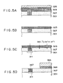
- the flattening agent 326 was coated.
- a resist of 1 to 5cp, or an inorganic type SOG was employed, and coated to about 2000 A (Fig. 3C).
- the peripheral portion is separated with an oxidized film, and therefore the alignment margin can be also made larger.
- Fig. 4 shows h FE for the emitter size of the bipolar transistor formed by use of this Example, and for that of the prior art type bipolar transistor.
- the emitter size dependency has become smaller by use of this Example. Further, when compared with the bipolar transistor of the same size, h FE variance becomes smaller.
- the emitter of the bipolar transistor is made finer, by utilizing the present invention, it becomes possible to form polycrystalline silicon with different film thicknesses on the emitter portion and the field.
- Fig. 6A and Fig. 6B are schematic sectional views for illustration of the Example when the simultaneous preparation process of the present invention was used in the case of forming two kinds of transistors with different window opening dimensions, respectively.
- the present invention can be expected to give further greater effect in the bipolar transistor utilizing the potential barrier in the polycrystalline silicon.
- etching since impurity is introduced after etching, etching can be performed unifomly, and also the polycrystalline silicon remains only in the grooves subjected to window opening, and therefore the problem as mentioned above can be solved.
- Fig. 7A is a schematic partial sectional view of a transistor according to the preparation process of the prior art, in which 306 is the base region, 307 the interlayer insulating film, 353 the DOPOS region having low concentration impurity, 354 the DOPOS region having high concentration impurity, and 355 the resist.
- the sectional shape becomes disturbed by the grain size of the polycrystalline silicon, the impurity concentration.
- Fig. 7B is a schematic partial sectional view of a transistor according to the preparation process of the present invention, and as shown in the Figure, so far as the preparation process of the present invention is utilized, there exists no section as shown in Fig. 7A and therefore there is no problem as mentioned above.
- Fig. 8 is a schematic sectional view for illustration of an example in which the present invention is used for the emitter of a bipolar transistor.
- This Example as shown in the Figure, has the n embedded layer 402 for reducing the collector resistance of an NPN bipolar transistor formed on the silicon substrate 401, and the n- epitaxial layer 403 which becomes the collector formed thereafter.
- n layer 404 and the p layer 405 which becomes the element separation region in the same meaning as the n embedded layer 402 a thick oxidized layer 406 was formed on the surface, and subjected to patterning according to the photoetching method.
- a thin oxidized film 408 was formed.
- the polycrystalline silicon 409 was formed to about 0.2 ⁇ m at about 600 °C according to the low pressure CVD method.
- the heat treatment in the first step was conducted at 650 °C for one hour, and the heat treatment in the second step at about 800 °C to 900 °C for one hour, to form the n layer 410 which becomes the emitter.
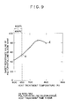
- Fig. 9 shows the heat treatment temperature and the sheet resistance value of the polycrystalline silicon when the heat treatment was carried out only once.
- a very low temperature of 650 °C by carrying out the heat treatment at a very low temperature of 650 °C, a low sheet resistance value is exhibited. This may be considered to be because the crystal grains become larger in this temperature region.
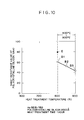
- Fig. 10 shows the relationship between the heat treatment temperature for the second time and the sheet resistance value of the polycrystalline silicon obtained from the Example. Also, for the purpose reference, the values when the heat treatment was carried out only once (800 °C, one hour) are shown by the point E.
- the points B1 to B3 in the Figure respectively show the results of the present embodiment, but as shown in the Figure, according to this Example, the sheet resistance value of the polycrystalline silicon could be reduced.
- arsenic was employed as the impurity in the polycrystalline silicon, but it may be also phosphorus. Also, the present invention is effective as the means for lowering resistance when the polycrystalline silicon is used as wiring or the gate electrode of MOS transistor.
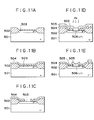
- the base of p 503 was formed by ion injection through the gate oxidized film region (Fig. 11A).
- the Si0 2 film 504 was deposited with a thickness of about 1000 A or more at a temperature of about 400 °C (Fig. 11 B). The thickness of the Si0 2 film 504 was set at a thickness to the extent which can prevent the thickness of the base surface from changing by thrusting the impurity (As in this example) ion injected into the polycrystalline silicon in the subsequent steps.
- the injected amount of As was made the condition of making the polycrystalline silicon amorphous, and in the case of As, 3E14/cm 2 or higher. Then, by patterning of the polycrystalline silicon layer, the emiter 506 of DOPOS BPT was formed (Fig. 11 E).
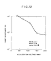
- Fig. 12 shows the relationship between the acceleration voltage of As ion injection and the sheet resistance value of the polycrystalline silicon.
- the injected amount is 5E15/cm 2 or more, the film thickness of the polycrystalline silicon 2000A, the heat treatment conditions 800 °C, one hour.
- a device having a sheet resistance value lower to great exent than the conditions of low acceleration voltage of the prior art was obtained.
- amorphous formation is effected to a depth of the As concentration of about 2E19/cm 2.
- the depth of the amorphous layer Xc is about 1600 ⁇ , and therefore when the film thickness of the polycrystalline silicon is made t, the sheet resistance will be abruptly reduced if the condition of 0.8t Xc is satisfied.
- Fig. 13 shows the relationship between the heat treatment temperature after As ion injection and the sheet resistance value of the polycrystalline silicon.
- the injected amount is 5E15/cm 2 , the acceleration voltage 150 keV, the film thickness of the polycrystalline silicon 2000 ⁇ , the heat treatment conditions 800 °C, 1 hour.
- a low sheet resistance value was obtained at a low temperature of 650 °C.
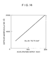
- Fig. 14 shows the relationship between the acceleration voltage and the depth Xc of the amorphous layer in the case of As(Ge) ion injection.
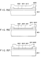
- Figs. 15A to 15F are respectively schematic sectional views for illustration of the primary preparation steps of the silicon-npn bipolar transistor which is an example of the present invention.
- Figs. 16 to 18 are respectively graphs showing the temperatures states in the first heat treatment and the second heat treatment.
- the above preparation steps can be also carried out without separation into the step (e) and the step (f), but successively according to continuous temperature elevation as shown in Fig. 17 or according to stepwise temperature elevation as shown in Fig. 18.
- the first heat treatment is carried out on the lower temperature side in the Figure and the second heat treatment on the higher temperature side in the Figure.
- step (f) may be also replaced with the heat treatment at a high temperature (for example, 1000 °C), within a short time (for example 10 seconds) according to the Rapid Thermal Anneal (RTA) method.
- a high temperature for example, 1000 °C
- RTA Rapid Thermal Anneal
- the polycrystal is a mass of monocrystals having a distribution in sizes, with the crystal grain having no constant crystal direction. And, the respective crystal grains have a crystal grain boundary which is the mutual grain boundary, having there a remarkable disturbance of lattice there. The presence of such crystal grain boundary is a cause for the polycrystal having different characteristics from monocrystal.
- diffusion in the polycrystal can be classified largely into the diffusion through the crystal grain boundary (diffusion constant Dg b ) and the diffusion within each crystal grain (diffusion constant Dg), and the whole effective diffusion constant Dell is represented by the following formula.
- f is the ratio of the impurity species existing in the crystal grain boundary, and as a model, in the case of a cubic grain size, In the formula, k: segregation coefficient to grain boundary, delta:crystal grain boundary width, Lg:crystal grain size.
- the value of k is generally 1 or more, namely a value of about 20 to 1250.
- delta is ca. 5A
- Lg is determined on the polycrystal deposition conditions, being 100 A to some 1000 ⁇ .
- Dg b » Dg In the case of a polycrystal, ordinarily Dg b » Dg.
- the relationship between Dell and D is Dell » D.
- Fig. 19 is a graph showing the diffusion coefficient for the n-type impurity.
- the axis of abscissa is 1000/T (°K) and the axis of ordinate the diffusion coefficient ( ) (um/hr 1/2 ).
- the diffusion coefficient (D) in the monocrystal is shown for the impurities As, Bi and P
- the effective diffusion coefficient (D eff ) represented by the mark x
- the diffusion coefficient of the grain boundary (D g ) represented by the mark A
- the diffusion coefficient (D) in the monocrystal of As and the effective diffusion coefficient (D eff and the grain boundary diffusion coefficient (D g ) in the polycrystal are respectively different by about 10-fold.
- Fig. 20 is a graph showing the diffusion coefficients of the p-type impurity.
- the diffusion coefficient (D) in the monocrystal is shown for the impurities Al, B, Ga, In, TI, and the effective diffusion coefficient (D eff ) (indicated by the mark x) and the grain boundary diffusion coefficient (D g ) (indicated by the mark A) in the polycrystal are shown for the impurity B.
- the respective diffusion coefficients for the impurity B are also clearly different by about 1 figure in the order of (D « D eff « D gb ).
- the segregation coefficient k is the ratio of the impurity occupying the site of the grain boundary to the ratio of the impurity occupying the site in the crystal grain, and depends on the kind, the concentration, the temperature, the grain size, etc. of the impurity, but qualitatively becomes smaller in the case of high concentration and in the case of high temperature. As, P, etc. have larger coefficients, while B has smaller coefficient. An example is shown in Table 1 (which is, however, different depending on the literature).
- Fig. 21 is a graph showing the coefficients of the impurities in the Si0 2 monocrystal, this showing an example when the diffusion constant speed is slow.
- the axis of abscissa is 1000/T ( O K- 1 ), and the axis of ordinate (D) (u/hr 1/2 ).
- the impurities shown are As and P.
- the grain boundary is necessarily formed between the Si0 2 and the polycrystalline silicon Si.
- Fig. 22 is an enlarged view of the polycrystalline Si deposited layer 610, the tunnel oxidied film 601 and the monocrystalline Si substrate 601 shown in Fig. 15.
- the impuriy ion injected into the polycrystalline Si deposited layer 610 will be mostly diffused along the grain boundary 607A (shown by the arrowhead V), because the diffusion coefficient of the boundary ( v lDg b ) is larger by 10-fold or more as compared with the diffusion coefficient within the crystal grain ( v lDg). Also, since the segregation coefficient is also large in the grain boundary 607A, high concentration region is formed along the grain boundary 607A. Since there is similarly a grain boundary also between the tunnel oxidized film 601 and the polycrystalline Si deposited layer 610, the impurity will be quickly diffused also into the grain boundary 607C (shown by the arrowhead H).
- Fig. 23 is a graph showing the relationship between the film thickness of the oxidized film and the time when forming an oxidized film by injection of oxygen according to the Rapid Thermal Anneal method (RTA).
- RTA Rapid Thermal Anneal method
- the axis of abscissa is time (sec.) and the axis of ordinate is film thickness (A).
- the parameter is temperature (°C)
- the film can be formed with good reproducibility at a film thickness of 10 A or more, and therefore formed stably.
- the material which can be made the diffusion barrier as described above not only Si0 2 , but also Sb N 4 , SiC, etc. with smaller impurity diffusion speed than the polycrystalline Si similarly as Si0 2 may be employed.
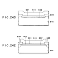
- Figs. 24A to 24E are respectively schematic sectional views for illustration of the preparation steps of the silicon-npn bipolar transistor of Example 8 of the present invention.
- the base and emitter layer could be formed self-matchingly.
- various diffused layers could be formed.
- the electrode can be also taken out by preparing previously the external base region 620 at the peripheral of the base.
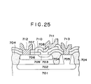
- Example 9 is now described by referring to Fig. 25.
- 701 is a p-type silicon substrate, 702 an n-type impurity region such as As or Sb, 703 an n-type epitaxial region, 704 an element separation region, 705 an n-type impurity region provided for collector resistance reduction, 706 a base region, 707 an interlayer insulating layer, 708 a polycrystalline silicon region with large grain size containing an n-type impurity, 709 an n-type emitter region formed by the polycrystalline silicon region 708, 710 an interlayer insulating film, 711 an electrode wiring of emitter, 712 an electrode wiring of base, 713 an electrode wiring of collector.
- 701 is a p-type silicon substrate
- 702 an n-type impurity region such as As or Sb
- 703 an n-type epitaxial region
- 704 an element separation region
- 705 an n-type impurity region provided for collector resistance reduction
- 706 a base
- a p-type silicon substrate containing a p-type impurity such as boron etc. at a concentration of about 1 E15 to 1 E17 cm-3 was thermally oxidized to form an oxidized film with a thickness of about 3000 A to 1 ⁇ m.
- photholithographic treatment was applied and the oxidized film at the desired site was removed by etching.
- oxidation treatment was again applied to form an oxidized film with a thickness of about 1000 ⁇ .
- heat treatment for activation was applied.
- the epitaxial layer had a thickness of about 2 to 10 ⁇ m, containing P, As, etc. at a concentration of about lEl4 to 1E16 cm- 3 .
- the substantial epitaxial layer thickness which depends also on its formation conditions, is 5 ⁇ m or less (Fig. 26A).
- the substrate is thermally oxidized to be coated with a nitrided film, and then the nitrided film and the oxidized film at the desired sites were removed. With the remaining nitrided film as the mask, the substrate was etched and subsequently thermal oxidizing treatment was applied, whereby a thick oxidized film 704 was formed only at the element separation region. Then, by repeating resist mask patterning, ion injection and resist peeling, the regions 705 and 706 were formed (Fig. 26B).
- the polycrystalline region 708 and the emitter region 709 were formed.
- the oxidized film at the desired site was removed by etching and the polycrystalline silicon coated with a thickness of about 1000 to 5000 ⁇ . Formation of the polycrystalline silicon at this time could be done by use of an He-SiH 4 system gas at a temperature of 600 to 700 °C. When formed in this temperature region, the growth speed could be taken sufficiently great (about 100 A/min.) and a stable polycrystalline silicon obtained.
- the next steps is the step of ion injection at a concentration of about 1E18 to 1E20 cm- 3 for introduction of an impurity.
- the ion species may be of the n-type, and As or P can be advantageously used.
- a uniform diffusion depth could be obtained.
- the amorphous layer film thickness is 2000 ⁇
- the tail of the imprity is penetrated into the substrate at 130 KeV or higher for As, and at 80 KeV or higher for P.
- the region 708 comprising a polycrystalline silicon with large grain sizes could be formed (Fig. 26C).
- a film such as of nitrided sulfur glass (NSG), phosphorus glass (PSG) was formed by use of the CVD method, applied with window opening, followed by electrode formation. By doing so, the semiconductor device shown in Fig. 25 is obtained.
- the region 709 may be also formed by first forming an amorphous silicon layer with a thickness of, for example, 1000 A to 5000 ⁇ , and then injecting inactive ions into the layer.
- the acceleration voltage during ion injection may be chosen to an appropriate value depending on the thickness of the amorphous layer.
- Fig. 28 shows the relationship between the thickness of the amorphous layer and the acceleration voltage when the ion species is Si 28. For example, if it is a polycrystalline silicon with a thickness of 2000 ⁇ , the appropriate acceleration voltage is about 200 KeV.
- the treatments of heat treatment et seq are performed in the same manner as in the foregoing Examples. Since the nucleus density is further reduced by injection of such inactive ions, recrystallization from the substrate will more readily occur. Amorphous formation to substantially the same extent is effected when Ge or C is employed other than Si as the inactive ions.
- the diffused layer of the emitter region becomes uniform in fine bipolar transistor, whereby a transistor with uniform and stable characteristics can be obtained.
- the present invention is excellent with respect to flattening, and therefore can be an effective means for making the device finer.
- the present invention can form the devices by means of the preparation device of the prior art, and is also excellent in bulk productivity, etc.
- the present invention by ion injecting the above-mentioned impurity so that the thickness t of the polycrystalline semiconductor region and the thickness Xc of the above-mentioned amorphous region may become the relationship of 0.8 t Xc, a semiconductor device of low resistance can be easily obtained, and also the heat treatment can be carried out at a low temperature of 600 ° C to 650 ° C.
- the formation speed of the polycrystalline silicon may be slightly lowered, by lowering of the formation temperature, it has become possible to obtain a low resistance value which could not be achieved in the prior art technique in a low temperature process.
- variance of h FE could be inhibited to about 1/3 as compared with DOPOS BPT obtained in the prior art method, and further the series resistance of emitter reduced to 1/3 to 1/5.
- injection of an impurity from the polycrystalline layer to the substrate is done through a thin film, and therefore recrystallization of polycrystal and damaging of naturally oxidized film by heat treatment and damaging of the junctioned face by ion injection can be prevented, whereby the junctioned face of the diffused layers formed in the substrate can be made a uniform and stable junctioned face. Accordingly, it becomes possible to form a very thin diffused layer suitable for higher integration.
- a process for preparing a semiconductor device comprises exposing at least a part of the main surface of a semiconductor substrate, forming a layer comprising the same main component as the above substrate, forming a flattening agent layer on the surface of said layer, removing the above layer and the flattening agent layer at the same time and injecting an impurity after said removing step.
Landscapes
- Bipolar Transistors (AREA)
- Weting (AREA)
Applications Claiming Priority (10)
| Application Number | Priority Date | Filing Date | Title |
|---|---|---|---|
| JP235894/90 | 1990-09-07 | ||
| JP235893/90 | 1990-09-07 | ||
| JP2235894A JPH04116923A (ja) | 1990-09-07 | 1990-09-07 | 半導体装置の製造方法 |
| JP2235893A JP2854947B2 (ja) | 1990-09-07 | 1990-09-07 | 半導体装置の製造方法 |
| JP257248/90 | 1990-09-28 | ||
| JP2257248A JPH04137619A (ja) | 1990-09-28 | 1990-09-28 | 半導体装置の製造方法 |
| JP326052/90 | 1990-11-29 | ||
| JP2326052A JPH04199634A (ja) | 1990-11-29 | 1990-11-29 | 半導体装置の製造方法 |
| JP20269/91 | 1991-01-22 | ||
| JP3020269A JPH04237118A (ja) | 1991-01-22 | 1991-01-22 | 半導体装置の製造方法 |
Publications (2)
| Publication Number | Publication Date |
|---|---|
| EP0480178A2 true EP0480178A2 (fr) | 1992-04-15 |
| EP0480178A3 EP0480178A3 (en) | 1992-11-19 |
Family
ID=27520217
Family Applications (1)
| Application Number | Title | Priority Date | Filing Date |
|---|---|---|---|
| EP19910115132 Withdrawn EP0480178A3 (en) | 1990-09-07 | 1991-09-06 | Process for preparing semiconductor device |
Country Status (3)
| Country | Link |
|---|---|
| US (4) | US5242858A (fr) |
| EP (1) | EP0480178A3 (fr) |
| CA (1) | CA2050781C (fr) |
Cited By (4)
| Publication number | Priority date | Publication date | Assignee | Title |
|---|---|---|---|---|
| US6133126A (en) * | 1997-09-18 | 2000-10-17 | Siemens Aktiengesellschaft | Method for fabricating a dopant region |
| US6160279A (en) * | 1993-05-26 | 2000-12-12 | Semiconductor Energy Laboratory Co., Ltd. | Method for producing a semiconductor device including doping with a catalyst that is a group IV element |
| US6765229B2 (en) | 1993-05-26 | 2004-07-20 | Semiconductor Energy Laboratory Co., Ltd. | Method for producing semiconductor device |
| CN117711917A (zh) * | 2024-02-05 | 2024-03-15 | 中国科学院长春光学精密机械与物理研究所 | 一种多晶硅薄膜及其制备方法 |
Families Citing this family (38)
| Publication number | Priority date | Publication date | Assignee | Title |
|---|---|---|---|---|
| DE69424717T2 (de) * | 1993-03-17 | 2001-05-31 | Canon K.K., Tokio/Tokyo | Verbindungsverfahren einer Verdrahtung mit einem Halbleitergebiet und durch dieses Verfahren hergestellte Halbleitervorrichtung |
| JPH07221174A (ja) * | 1993-12-10 | 1995-08-18 | Canon Inc | 半導体装置及びその製造方法 |
| US6326248B1 (en) * | 1994-06-02 | 2001-12-04 | Semiconductor Energy Laboratory Co., Ltd. | Process for fabricating semiconductor device |
| JP3621151B2 (ja) * | 1994-06-02 | 2005-02-16 | 株式会社半導体エネルギー研究所 | 半導体装置の作製方法 |
| JPH0869967A (ja) * | 1994-08-26 | 1996-03-12 | Semiconductor Energy Lab Co Ltd | 半導体装置の作製方法 |
| US6331475B1 (en) | 1995-01-12 | 2001-12-18 | Semiconductor Energy Laboratory Co., Ltd. | Method and manufacturing semiconductor device |
| TW463378B (en) | 1995-06-01 | 2001-11-11 | Semiconductor Energy Lab | Method of manufacturing semiconductor device |
| US6750091B1 (en) * | 1996-03-01 | 2004-06-15 | Micron Technology | Diode formation method |
| US5792700A (en) * | 1996-05-31 | 1998-08-11 | Micron Technology, Inc. | Semiconductor processing method for providing large grain polysilicon films |
| JP3440698B2 (ja) * | 1996-06-24 | 2003-08-25 | ソニー株式会社 | 半導体装置の製造方法 |
| JP3450163B2 (ja) * | 1997-09-12 | 2003-09-22 | Necエレクトロニクス株式会社 | 半導体装置の製造方法 |
| US5960322A (en) * | 1997-12-19 | 1999-09-28 | Advanced Micro Devices, Inc. | Suppression of boron segregation for shallow source and drain junctions in semiconductors |
| US5904536A (en) * | 1998-05-01 | 1999-05-18 | National Semiconductor Corporation | Self aligned poly emitter bipolar technology using damascene technique |
| US6207493B1 (en) * | 1998-08-19 | 2001-03-27 | International Business Machines Corporation | Formation of out-diffused bitline by laser anneal |
| KR100379136B1 (ko) * | 1998-10-02 | 2003-04-08 | 인터내셔널 비지네스 머신즈 코포레이션 | 반도체 소자 형성 방법과 반도체 소자 |
| TW466758B (en) * | 1998-10-26 | 2001-12-01 | United Microelectronics Corp | Manufacturing method of flash memory |
| TW399235B (en) * | 1998-12-04 | 2000-07-21 | United Microelectronics Corp | Selective semi-sphere silicon grain manufacturing method |
| US6429101B1 (en) | 1999-01-29 | 2002-08-06 | International Business Machines Corporation | Method of forming thermally stable polycrystal to single crystal electrical contact structure |
| US6262472B1 (en) | 1999-05-17 | 2001-07-17 | National Semiconductor Corporation | Bipolar transistor compatible with CMOS utilizing tilted ion implanted base |
| US6043130A (en) * | 1999-05-17 | 2000-03-28 | National Semiconductor Corporation | Process for forming bipolar transistor compatible with CMOS utilizing tilted ion implanted base |
| US7838794B2 (en) | 1999-12-28 | 2010-11-23 | Gsi Group Corporation | Laser-based method and system for removing one or more target link structures |
| US6281471B1 (en) * | 1999-12-28 | 2001-08-28 | Gsi Lumonics, Inc. | Energy-efficient, laser-based method and system for processing target material |
| US7671295B2 (en) * | 2000-01-10 | 2010-03-02 | Electro Scientific Industries, Inc. | Processing a memory link with a set of at least two laser pulses |
| US20030222324A1 (en) * | 2000-01-10 | 2003-12-04 | Yunlong Sun | Laser systems for passivation or link processing with a set of laser pulses |
| US20060141681A1 (en) * | 2000-01-10 | 2006-06-29 | Yunlong Sun | Processing a memory link with a set of at least two laser pulses |
| US6309982B1 (en) * | 2001-03-12 | 2001-10-30 | Chartered Semiconductor Manufacturing Ltd. | Method for minimizing copper diffusion by doping an inorganic dielectric layer with a reducing agent |
| US6639177B2 (en) * | 2001-03-29 | 2003-10-28 | Gsi Lumonics Corporation | Method and system for processing one or more microstructures of a multi-material device |
| JP2003077854A (ja) * | 2001-09-05 | 2003-03-14 | Mitsubishi Electric Corp | 半導体装置の製造方法および半導体装置 |
| US7563695B2 (en) | 2002-03-27 | 2009-07-21 | Gsi Group Corporation | Method and system for high-speed precise laser trimming and scan lens for use therein |
| JP3484177B2 (ja) * | 2002-04-26 | 2004-01-06 | 沖電気工業株式会社 | 半導体装置とその製造方法 |
| US7687917B2 (en) * | 2002-05-08 | 2010-03-30 | Nec Electronics Corporation | Single damascene structure semiconductor device having silicon-diffused metal wiring layer |
| JP4012040B2 (ja) * | 2002-10-31 | 2007-11-21 | キヤノン株式会社 | センタタップ終端回路及びセンタタップ終端回路を有するプリント配線板 |
| US6825102B1 (en) * | 2003-09-18 | 2004-11-30 | International Business Machines Corporation | Method of improving the quality of defective semiconductor material |
| EP1622435A1 (fr) * | 2004-07-28 | 2006-02-01 | ATOTECH Deutschland GmbH | Méthode de fabrication d'un dispositif par des techniques d'écriture directe |
| US8242354B2 (en) * | 2008-12-04 | 2012-08-14 | Sunpower Corporation | Backside contact solar cell with formed polysilicon doped regions |
| TWI453939B (zh) | 2010-12-30 | 2014-09-21 | Au Optronics Corp | 太陽能電池及其製作方法 |
| KR102272433B1 (ko) * | 2015-06-30 | 2021-07-05 | 엘지전자 주식회사 | 태양 전지 및 이의 제조 방법 |
| JP6702268B2 (ja) * | 2017-06-15 | 2020-05-27 | 信越半導体株式会社 | エピタキシャルウェーハの製造方法 |
Family Cites Families (22)
| Publication number | Priority date | Publication date | Assignee | Title |
|---|---|---|---|---|
| US4041518A (en) * | 1973-02-24 | 1977-08-09 | Hitachi, Ltd. | MIS semiconductor device and method of manufacturing the same |
| US4378627A (en) * | 1980-07-08 | 1983-04-05 | International Business Machines Corporation | Self-aligned metal process for field effect transistor integrated circuits using polycrystalline silicon gate electrodes |
| DE3280219D1 (de) * | 1981-03-11 | 1990-08-30 | Fujitsu Ltd | Verfahren zur herstellung einer halbleiteranordnung mit ausgluehen eines halbleiterkoerpers. |
| JPS6084825A (ja) * | 1983-10-14 | 1985-05-14 | Seiko Epson Corp | 半導体装置の製造方法 |
| FR2566181B1 (fr) * | 1984-06-14 | 1986-08-22 | Commissariat Energie Atomique | Procede d'autopositionnement d'une ligne d'interconnexion sur un trou de contact electrique d'un circuit integre |
| FR2568723B1 (fr) * | 1984-08-03 | 1987-06-05 | Commissariat Energie Atomique | Circuit integre notamment de type mos et son procede de fabrication |
| US4708767A (en) * | 1984-10-05 | 1987-11-24 | Signetics Corporation | Method for providing a semiconductor device with planarized contacts |
| JPH0824184B2 (ja) * | 1984-11-15 | 1996-03-06 | ソニー株式会社 | 薄膜トランジスタの製造方法 |
| US4617066A (en) * | 1984-11-26 | 1986-10-14 | Hughes Aircraft Company | Process of making semiconductors having shallow, hyperabrupt doped regions by implantation and two step annealing |
| US4676847A (en) * | 1985-01-25 | 1987-06-30 | American Telephone And Telegraph Company At&T Bell Laboratories | Controlled boron doping of silicon |
| US4604150A (en) * | 1985-01-25 | 1986-08-05 | At&T Bell Laboratories | Controlled boron doping of silicon |
| JPS61208829A (ja) * | 1985-03-14 | 1986-09-17 | Matsushita Electric Ind Co Ltd | 半導体装置の製造方法 |
| FR2582445B1 (fr) * | 1985-05-21 | 1988-04-08 | Efcis | Procede de fabrication de transistors mos a electrodes de siliciure metallique |
| US4707456A (en) * | 1985-09-18 | 1987-11-17 | Advanced Micro Devices, Inc. | Method of making a planar structure containing MOS and bipolar transistors |
| IT1209682B (it) * | 1985-12-23 | 1989-08-30 | Sgs Microelettronica Spa | Processo per la fabbricazione mediante ricristallizzazione epitassiale di transistori ad effetto di campo a gate isolato con giunzioni a profondita' minima. |
| US4697328A (en) * | 1986-04-28 | 1987-10-06 | Rockwell International Corporation | Method of making hardened NMOS sub-micron field effect transistors |
| FR2599182B1 (fr) * | 1986-05-21 | 1991-10-31 | Telemecanique Electrique | Procede et dispositif de commande d'un electro-aimant dont l'excitation, par un courant alternatif, provoque la mise en contact de deux pieces |
| JPS6310573A (ja) * | 1986-07-02 | 1988-01-18 | Oki Electric Ind Co Ltd | 半導体装置の製造方法 |
| US4939154A (en) * | 1987-03-25 | 1990-07-03 | Seiko Instruments Inc. | Method of fabricating an insulated gate semiconductor device having a self-aligned gate |
| US4871684A (en) * | 1987-10-29 | 1989-10-03 | International Business Machines Corporation | Self-aligned polysilicon emitter and contact structure for high performance bipolar transistors |
| JPH07118448B2 (ja) * | 1988-02-05 | 1995-12-18 | 松下電子工業株式会社 | 半導体装置の製造方法 |
| GB8810973D0 (en) * | 1988-05-10 | 1988-06-15 | Stc Plc | Improvements in integrated circuits |
-
1991
- 1991-09-05 US US07/755,452 patent/US5242858A/en not_active Expired - Fee Related
- 1991-09-06 CA CA002050781A patent/CA2050781C/fr not_active Expired - Fee Related
- 1991-09-06 EP EP19910115132 patent/EP0480178A3/en not_active Withdrawn
-
1993
- 1993-05-27 US US08/067,788 patent/US5476799A/en not_active Expired - Fee Related
-
1995
- 1995-02-17 US US08/390,548 patent/US5597741A/en not_active Expired - Fee Related
- 1995-06-01 US US08/457,149 patent/US5739590A/en not_active Expired - Fee Related
Cited By (5)
| Publication number | Priority date | Publication date | Assignee | Title |
|---|---|---|---|---|
| US6160279A (en) * | 1993-05-26 | 2000-12-12 | Semiconductor Energy Laboratory Co., Ltd. | Method for producing a semiconductor device including doping with a catalyst that is a group IV element |
| US6765229B2 (en) | 1993-05-26 | 2004-07-20 | Semiconductor Energy Laboratory Co., Ltd. | Method for producing semiconductor device |
| US6133126A (en) * | 1997-09-18 | 2000-10-17 | Siemens Aktiengesellschaft | Method for fabricating a dopant region |
| CN117711917A (zh) * | 2024-02-05 | 2024-03-15 | 中国科学院长春光学精密机械与物理研究所 | 一种多晶硅薄膜及其制备方法 |
| CN117711917B (zh) * | 2024-02-05 | 2024-05-28 | 中国科学院长春光学精密机械与物理研究所 | 一种多晶硅薄膜及其制备方法 |
Also Published As
| Publication number | Publication date |
|---|---|
| CA2050781C (fr) | 1997-11-18 |
| US5739590A (en) | 1998-04-14 |
| US5242858A (en) | 1993-09-07 |
| US5476799A (en) | 1995-12-19 |
| CA2050781A1 (fr) | 1992-03-08 |
| US5597741A (en) | 1997-01-28 |
| EP0480178A3 (en) | 1992-11-19 |
Similar Documents
| Publication | Publication Date | Title |
|---|---|---|
| EP0480178A2 (fr) | Procédé de préparation d'un composant semi-conducteur | |
| US4717681A (en) | Method of making a heterojunction bipolar transistor with SIPOS | |
| US4375999A (en) | Method of manufacturing a semiconductor device | |
| US4101350A (en) | Self-aligned epitaxial method for the fabrication of semiconductor devices | |
| CA1142267A (fr) | Structure a transistors complementaires et methode de fabrication | |
| US6713359B1 (en) | Semiconductor device and method of manufacturing the same including raised source/drain comprising SiGe or SiC | |
| US4875085A (en) | Semiconductor device with shallow n-type region with arsenic or antimony and phosphorus | |
| US7851890B2 (en) | Semiconductor device and method for manufacturing the same | |
| EP0033495B1 (fr) | Procédé de fabrication d'un transistor bipolaire à grande vitesse | |
| US4597167A (en) | Method of forming a metal film on a selectively diffused layer | |
| US4460417A (en) | Method of manufacturing insulating film and electric device utilizing the same | |
| US5846869A (en) | Method of manufacturing semiconductor integrated circuit device | |
| JP2855919B2 (ja) | 半導体装置およびその製造方法 | |
| US4029527A (en) | Method of producing a doped zone of a given conductivity type in a semiconductor body | |
| US6184098B1 (en) | Field effect transistor device and method of manufacturing the same | |
| EP0042380B1 (fr) | Procédé permettant d'obtenir un profil de concentration d'impuretés ideal dans la base d'un transistor | |
| JP3457532B2 (ja) | 半導体装置の製造方法 | |
| GB1593694A (en) | Method for making a semiconductor device | |
| GB2137019A (en) | Semiconductor Device and Method for Manufacturing | |
| JP3006396B2 (ja) | 半導体薄膜の形成方法 | |
| US6673703B2 (en) | Method of fabricating an integrated circuit | |
| JP2797200B2 (ja) | 多結晶シリコン電極およびその製造方法 | |
| JPH1098187A (ja) | 半導体装置の製造方法 | |
| JP3114224B2 (ja) | 半導体装置の製造方法 | |
| JPH0831468B2 (ja) | 半導体装置の製造方法 |
Legal Events
| Date | Code | Title | Description |
|---|---|---|---|
| PUAI | Public reference made under article 153(3) epc to a published international application that has entered the european phase |
Free format text: ORIGINAL CODE: 0009012 |
|
| AK | Designated contracting states |
Kind code of ref document: A2 Designated state(s): DE FR GB IT NL |
|
| PUAL | Search report despatched |
Free format text: ORIGINAL CODE: 0009013 |
|
| AK | Designated contracting states |
Kind code of ref document: A3 Designated state(s): DE FR GB IT NL |
|
| 17P | Request for examination filed |
Effective date: 19930405 |
|
| 17Q | First examination report despatched |
Effective date: 19970312 |
|
| GRAP | Despatch of communication of intention to grant a patent |
Free format text: ORIGINAL CODE: EPIDOSNIGR1 |
|
| STAA | Information on the status of an ep patent application or granted ep patent |
Free format text: STATUS: THE APPLICATION IS DEEMED TO BE WITHDRAWN |
|
| 18D | Application deemed to be withdrawn |
Effective date: 20050518 |