EP0480201A1 - Circuit d'attaque de sortie de puce - Google Patents
Circuit d'attaque de sortie de puce Download PDFInfo
- Publication number
- EP0480201A1 EP0480201A1 EP91115603A EP91115603A EP0480201A1 EP 0480201 A1 EP0480201 A1 EP 0480201A1 EP 91115603 A EP91115603 A EP 91115603A EP 91115603 A EP91115603 A EP 91115603A EP 0480201 A1 EP0480201 A1 EP 0480201A1
- Authority
- EP
- European Patent Office
- Prior art keywords
- transistor
- channel
- field effect
- gate electrode
- driver circuit
- Prior art date
- Legal status (The legal status is an assumption and is not a legal conclusion. Google has not performed a legal analysis and makes no representation as to the accuracy of the status listed.)
- Withdrawn
Links
- 230000005669 field effect Effects 0.000 claims abstract description 34
- 230000005540 biological transmission Effects 0.000 claims abstract description 13
- 239000000758 substrate Substances 0.000 claims description 17
- 239000004065 semiconductor Substances 0.000 claims description 9
- 230000008878 coupling Effects 0.000 claims 1
- 238000010168 coupling process Methods 0.000 claims 1
- 238000005859 coupling reaction Methods 0.000 claims 1
- 230000015654 memory Effects 0.000 description 6
- 238000005516 engineering process Methods 0.000 description 5
- 238000009413 insulation Methods 0.000 description 3
- VYPSYNLAJGMNEJ-UHFFFAOYSA-N Silicium dioxide Chemical compound O=[Si]=O VYPSYNLAJGMNEJ-UHFFFAOYSA-N 0.000 description 2
- 238000010586 diagram Methods 0.000 description 2
- 239000012535 impurity Substances 0.000 description 2
- 238000000034 method Methods 0.000 description 2
- ZOXJGFHDIHLPTG-UHFFFAOYSA-N Boron Chemical compound [B] ZOXJGFHDIHLPTG-UHFFFAOYSA-N 0.000 description 1
- 229910052785 arsenic Inorganic materials 0.000 description 1
- RQNWIZPPADIBDY-UHFFFAOYSA-N arsenic atom Chemical compound [As] RQNWIZPPADIBDY-UHFFFAOYSA-N 0.000 description 1
- 229910052796 boron Inorganic materials 0.000 description 1
- 230000015556 catabolic process Effects 0.000 description 1
- 230000000295 complement effect Effects 0.000 description 1
- 230000001419 dependent effect Effects 0.000 description 1
- 238000009792 diffusion process Methods 0.000 description 1
- BHEPBYXIRTUNPN-UHFFFAOYSA-N hydridophosphorus(.) (triplet) Chemical compound [PH] BHEPBYXIRTUNPN-UHFFFAOYSA-N 0.000 description 1
- 238000005468 ion implantation Methods 0.000 description 1
- 229910044991 metal oxide Inorganic materials 0.000 description 1
- 150000004706 metal oxides Chemical class 0.000 description 1
- 230000003071 parasitic effect Effects 0.000 description 1
- 229910052710 silicon Inorganic materials 0.000 description 1
- 239000010703 silicon Substances 0.000 description 1
- 235000012239 silicon dioxide Nutrition 0.000 description 1
- 239000000377 silicon dioxide Substances 0.000 description 1
- 230000007704 transition Effects 0.000 description 1
Images
Classifications
-
- H—ELECTRICITY
- H03—ELECTRONIC CIRCUITRY
- H03K—PULSE TECHNIQUE
- H03K19/00—Logic circuits, i.e. having at least two inputs acting on one output; Inverting circuits
- H03K19/003—Modifications for increasing the reliability for protection
- H03K19/00315—Modifications for increasing the reliability for protection in field-effect transistor circuits
-
- H—ELECTRICITY
- H03—ELECTRONIC CIRCUITRY
- H03K—PULSE TECHNIQUE
- H03K19/00—Logic circuits, i.e. having at least two inputs acting on one output; Inverting circuits
- H03K19/02—Logic circuits, i.e. having at least two inputs acting on one output; Inverting circuits using specified components
- H03K19/08—Logic circuits, i.e. having at least two inputs acting on one output; Inverting circuits using specified components using semiconductor devices
- H03K19/094—Logic circuits, i.e. having at least two inputs acting on one output; Inverting circuits using specified components using semiconductor devices using field-effect transistors
- H03K19/0944—Logic circuits, i.e. having at least two inputs acting on one output; Inverting circuits using specified components using semiconductor devices using field-effect transistors using MOSFET or insulated gate field-effect transistors, i.e. IGFET
- H03K19/0948—Logic circuits, i.e. having at least two inputs acting on one output; Inverting circuits using specified components using semiconductor devices using field-effect transistors using MOSFET or insulated gate field-effect transistors, i.e. IGFET using CMOS or complementary insulated gate field-effect transistors
Definitions
- This invention relates to off-chip driver circuits and, more particularly, to a complementary metal oxide semiconductor (CMOS) off-chip driver circuit which is part of a system wherein the off-chip driver circuit is designed in a lower supply voltage environment than is the circuit to which the output of the off-chip driver circuit is connected.
- CMOS complementary metal oxide semiconductor
- Reduced scaling or shrinking of the geometries of devices used in integrated semiconductor circuit technology for forming denser circuits has required voltage supply sources to provide lower voltages than the heretofore generally accepted standard supply voltage of 5 volts so as to avoid a voltage breakdown in the smaller devices.
- a mix of circuits is being used wherein some of the circuits have been designed for use with standard 5 volt supplies while other circuits have been designed for use with the lower 3.3 to 3.6 volt supplies.
- the geometries of memory circuits are reduced at a faster rate than are the geometries of logic circuits which are coupled to the memory circuits.
- CMOS random access memories are currently being designed in about 3.3 to 3.6 volt supply technology
- logic circuits such as those of transistor-transistor logic (TTL) type, which receive the output signals or data from the memories, are still being designed in a 5 volt supply technology.
- TTL transistor-transistor logic
- U.S. Patent No. 4,217,502 filed Sept. 11, 1978, discloses a circuit similar to that of the hereinabove identified U.S. Patent 4,585,958 but additionally provides voltage control of the P-channel transistor substrate.
- the invention provides a driver circuit having higher performance and higher density of devices, which interfaces between a first circuit with a given supply voltage and a second circuit with a supply voltage having a magnitude greater than that of the given supply voltage without producing an excessive voltage stress on insulation or oxide layers in any of the devices of the circuits and with minimum or no current leakage paths.
- an off-chip driver circuit which includes a pull up transistor - preferably a first P-channel field effect transistor - and a pull down transistor - preferably a first N-channel field effect transistor - serially arranged between a first voltage source having a supply voltage of a given magnitude and a point of reference potential, such as ground, with the common point between these transistors forming a data output terminal to which is connected a circuit including a second voltage source having a supply voltage of a magnitude significantly greater than that of the given magnitude.
- a second P-channel field effect transistor is connected between the data output terminal and the control or gate electrode of the first P-channel transistor.
- a first input terminal is coupled to the control or gate electrode of the first P-channel transistor through a transmission gate including a third P-channel field effect transistor arranged in parallel with a second N-channel field effect transistor, with the control or gate electrode of the third P-channel transistor being connected to the data output terminal and the control or gate electrode of the second N-channel transistor being connected to the first voltage source.
- a second input terminal is connected to the gate electrode of the first N-channel transistor. Means are also provided to appropriately bias the substrate of the first, second and third P-channel transistors.
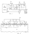
- FIG. 1 of the drawings there is shown a circuit diagram of a preferred embodiment of the CMOS off-chip driver circuit of the present invention connected to any suitable, known pre-driver circuit indicated by block 10 which may be of the type illustrated and described in the hereinabove identified commonly assigned U.S. Patent No. 4,782,250.
- the driver circuit being made in the CMOS technology, has its P-channel field effect transistors indicated by a rectangle with a diagonal line formed therein and a gate electrode arranged adjacent thereto and its N-channel field effect transistors indicated by a rectangle without a diagonal line and a gate electrode arranged adjacent thereto.
- the CMOS off-chip driver circuit of the present invention illustrated in FIG. 1 includes first and second input terminals IN and IN', respectively, connected to the pre-driver circuit 10, and a first P-channel field effect transistor 12 acting as a pull up transistor and a first N-channel field effect transistor 14 acting as a pull down transistor serially arranged between a first voltage source Vdd having a supply voltage of a given magnitude, such as 3.6 volts, and a point of reference potential, such as ground.
- the common point between the serially arranged transistors 12 and 14 forms a data output terminal Vout.
- the gate electrode of the first N-channel transistor is connected to the second input terminal IN'.
- a second P-channel field effect transistor 16 acting as a control transistor is connected between the output terminal Vout and the gate electrode of the first P-channel transistor 12 with its gate electrode connected to a reference voltage Vc which has a magnitude preferably equal to or less than the supply voltage of the first voltage source Vdd and equal to or greater than the supply voltage of the first voltage source Vdd minus the threshold voltage Vt of the P-channel transistor 12. It can be seen that it is convenient to have the voltage Vc be made equal to that of the first voltage source Vdd.
- a third P-channel field effect transistor 18 acting as an N-well bias transistor is connected between the first voltage source Vdd and a common N-well 20 with its gate electrode being connected to the data output terminal Vout.
- the P-channel pull up transistor 12, control transistor 16 and N-well bias transistor 18 are all disposed in the common N-well 20, as can be seen more readily in FIG. 2 of the drawings, which will be discussed hereinbelow in more detail.
- a transmission gate 22 is connected between the first input terminal IN and the gate electrode of the pull up transistor 12.
- the transmission gate 22 includes a second N-channel field effect transistor 24 having its gate electrode connected to a point of reference potential, preferably the supply voltage of the first voltage source Vdd, and a fourth P-channel field effect transistor 26 connected in parallel with the second N-channel transistor having its gate electrode connected to the data output terminal Vout.
- An external circuit or system which may be a transistor-transistor logic (TTL) circuit having a second voltage source, sometimes known as VH, with a supply voltage of about 5 volts, indicated by block 28, is selectively connectable by any appropriate means, such switching means 30, to the data output terminal Vout.
- TTL transistor-transistor logic
- the external circuit or system 28 is generally formed on a separate semiconductor chip and may have voltages which range from about 0 to 5.5 volts.
- FIG. 2 of the drawings there is shown in cross-sectional view through a P-type semiconductor substrate 32, preferably made of silicon, the P-channel transistors 12, 16, 18 and 26 disposed in the common N-well 20, with the N-channel transistors 14 and 24 being formed in the P-type substrate 32.
- a gate oxide 34 preferably a thin layer of silicon dioxide, is grown on the surface of the substrate 32 to separate the gate electrodes of the transistors, i.e., transistors 12, 14, 16, 18, 24 and 26, from the surface of the substrate 32.
- the sources and drains of the P-channel transistors may be made by using diffusion or ion implantation techniques with, e.g., boron as the impurity, to form the P + regions in the common N-well 20, and the sources and drains of the N-channel transistors may be made by using these techniques with arsenic or phosphorous impurities to form the N + regions in the P-type semiconductor substrate 32.
- a contact to the common N-well 20 is made by forming an N + region in the N-well.
- output terminal Vout will be at a low voltage of approximately 0 volts.
- the output is in a high impedance state and the driver circuit is said to be disabled.
- voltages from the external circuit 28 which may have a magnitude of from 0 to 5.5 volts can be applied to the output terminal Vout with the closing of the switching means 30.
- the P-channel transistor 16 turns on allowing the voltage at the gate electrode of the first P-channel transistor 12 to rise to the voltage at the output terminal Vout. Forward biasing of the source-to-N-well junction of the P-channel transistor 16 causes current to flow into the N-well 20 and the floating N-well voltage consequently rises to the voltage at the output terminal Vout minus the base-emitter drop in the parasitic pnp transistor which is formed in the N-well 20.
- the P-channel transistor 12 which is also tied to the floating substrate or N-well 20, will now have a positive potential between its gate electrode and source, maintaining transistor 12 in the off condition to prevent current flow into the voltage source Vdd. Also, since the voltage at the gate electrode of the first P-channel transistor 12 is greater than the supply voltage of the voltage source Vdd minus a threshold voltage of the second N-channel transistor 24, transistor 24 turns off to prevent current flow into the pre-driver circuit 10. Of course, since the voltage at the output terminal Vout is high, the fourth P-channel transistor 26 of the transmission gate 22 will also be turned off.
- the transmission gate 22 which includes the P-channel transistor 26 with its gate electrode connected to the output terminal Vout and the N-channel transistor 24 with its gate electrode connected to the voltage source Vdd, a rail- to-rail voltage swing is provided which readily turns off the pull up transistor 12 to prevent current leakage into the voltage source Vdd when the voltage at the output terminal Vout is less than the supply voltage of the first voltage source Vdd plus the absolute value of the threshold voltage of the P-channel transistor 16.
- the driver circuit illustrated in FIGS. 1 and 2 of the drawings may be modified by eliminating the fourth P-channel transistor 26 of the transmission gate 22 and designing the transistors so that the supply voltage of the voltage source Vdd minus the threshold voltage of the N-channel transistor 24 is greater than the supply voltage of the voltage source Vdd minus the absolute value of the threshold voltage of the P-channel transistor 16 so as to pull the voltage at the gate electrode of the P-channel transistor 12 high enough to turn off the transistor 12.
- this invention provides a passgate between the pre-driver circuit 10 and the pull up transistor 12 in order to eliminate the need for disabling two of the P-channel transistors used in the prior art circuits, allowing implementation of logic controlled drivers without duplication of transistors.
- the pull up transistor 12 is turned off to prevent current flow into the first voltage source Vdd when a high voltage greater than a threshold voltage above the supply voltage Vdd is applied to the output terminal Vout, whereas in the prior art a second stacked transistor was required to prevent such current flow into the voltage source Vdd.
- the second stacked transistor of the prior art circuit requires a number of control transistors for typically data and enable inputs.
- each of the additional transistors would require a number of control transistors, as disclosed more fully in, e.g., IBM Technical Disclosure Bulletin, Vol. 33, No. 3A, August 1990, in an article entitled "Performance-Controlled CMOS Driver for Multi-Voltage Interfaces" by R. A. Piro. Accordingly, it can be seen that the driver circuit of the present invention can be operated with many fewer transistors and it does not require very large output transistors as pull up and pull down transistors, thus, resulting in the use of a significantly smaller substrate or chip area.
- the pull up transistor is used to block flowback current into the first voltage source Vdd without the need for a second stacked transistor as used in the prior art, and where stacked transistors are required for logic purposes the associated control transistors are not needed.
- This invention further allows a driver circuit not originally designed to operate with higher voltage networks to be converted for use with such networks with relative ease by simply adding three or four transistors, such as transistors 16, 18, 24 and 26 into a non-interfacing driver circuit.
- the CMOS off-chip driver circuit may also be formed in an N-type semiconductor substrate with the well being of the P-well type with all polarities reversed.
- an improved off-chip driver circuit for interface to higher voltage networks or circuits which uses fewer transistors to eliminate current leakage, has superior performance and requires a smaller surface area on a substrate or chip.
Landscapes
- Engineering & Computer Science (AREA)
- Physics & Mathematics (AREA)
- Computer Hardware Design (AREA)
- Computing Systems (AREA)
- General Engineering & Computer Science (AREA)
- Mathematical Physics (AREA)
- Power Engineering (AREA)
- Metal-Oxide And Bipolar Metal-Oxide Semiconductor Integrated Circuits (AREA)
- Logic Circuits (AREA)
Applications Claiming Priority (2)
| Application Number | Priority Date | Filing Date | Title |
|---|---|---|---|
| US595911 | 1990-10-11 | ||
| US07/595,911 US5151619A (en) | 1990-10-11 | 1990-10-11 | Cmos off chip driver circuit |
Publications (1)
| Publication Number | Publication Date |
|---|---|
| EP0480201A1 true EP0480201A1 (fr) | 1992-04-15 |
Family
ID=24385226
Family Applications (1)
| Application Number | Title | Priority Date | Filing Date |
|---|---|---|---|
| EP91115603A Withdrawn EP0480201A1 (fr) | 1990-10-11 | 1991-09-13 | Circuit d'attaque de sortie de puce |
Country Status (3)
| Country | Link |
|---|---|
| US (1) | US5151619A (fr) |
| EP (1) | EP0480201A1 (fr) |
| JP (1) | JPH07118644B2 (fr) |
Cited By (9)
| Publication number | Priority date | Publication date | Assignee | Title |
|---|---|---|---|---|
| FR2678451A1 (fr) * | 1991-06-28 | 1992-12-31 | Digital Equipment Corp | Circuit d'attaque de sortie cmos a puits flottant. |
| WO1994018755A1 (fr) * | 1993-02-10 | 1994-08-18 | National Semiconductor Corporation | Etage de sortie |
| EP0695037A1 (fr) * | 1994-07-25 | 1996-01-31 | STMicroelectronics Limited | Circuit d'attaque de sortie |
| EP0722223A3 (fr) * | 1995-01-14 | 1997-03-26 | Toshiba Kk | Circuit de sortie basse-tension pour dispositif semi-conducteur |
| EP0766400A1 (fr) * | 1995-09-26 | 1997-04-02 | Texas Instruments Incorporated | Etage de sortie supportant des surtensions extérieures appliquées sur sa sortie dans l'état haute impédance et non-alimenté |
| EP0630109B1 (fr) * | 1993-06-18 | 1998-08-26 | Texas Instruments Incorporated | Circuit d'attaque à faible excursion de tension de sortie |
| US5821796A (en) * | 1996-09-23 | 1998-10-13 | Texas Instruments Incorporated | Circuitry for providing a high impedance state when powering down a single port node |
| EP1102401A1 (fr) * | 1999-11-19 | 2001-05-23 | Intersil Corporation | Circuit d'attaque de bus et procédé de son opération |
| DE4404132C2 (de) * | 1993-02-10 | 2003-03-06 | Fairchild Semiconductor Corp N | Abschaltbare Vollausschlag-Pufferschaltung mit einer Isolierung bei mehrfacher Leistungsversorgung |
Families Citing this family (60)
| Publication number | Priority date | Publication date | Assignee | Title |
|---|---|---|---|---|
| US5675824A (en) * | 1992-09-30 | 1997-10-07 | Intel Corporation | Programmable logic having selectable output voltages |
| JP3478580B2 (ja) * | 1992-12-28 | 2003-12-15 | ヒュンダイ エレクトロニクス アメリカ | 出力駆動回路 |
| US5396128A (en) * | 1993-09-13 | 1995-03-07 | Motorola, Inc. | Output circuit for interfacing integrated circuits having different power supply potentials |
| US5453705A (en) * | 1993-12-21 | 1995-09-26 | International Business Machines Corporation | Reduced power VLSI chip and driver circuit |
| JP3562725B2 (ja) * | 1993-12-24 | 2004-09-08 | 川崎マイクロエレクトロニクス株式会社 | 出力バッファ回路、および入出力バッファ回路 |
| JP3311133B2 (ja) * | 1994-02-16 | 2002-08-05 | 株式会社東芝 | 出力回路 |
| US5451889A (en) * | 1994-03-14 | 1995-09-19 | Motorola, Inc. | CMOS output driver which can tolerate an output voltage greater than the supply voltage without latchup or increased leakage current |
| KR0120565B1 (ko) * | 1994-04-18 | 1997-10-30 | 김주용 | 래치-업을 방지한 씨모스형 데이타 출력버퍼 |
| US5786720A (en) * | 1994-09-22 | 1998-07-28 | Lsi Logic Corporation | 5 volt CMOS driver circuit for driving 3.3 volt line |
| US5467031A (en) * | 1994-09-22 | 1995-11-14 | Lsi Logic Corporation | 3.3 volt CMOS tri-state driver circuit capable of driving common 5 volt line |
| TW289153B (fr) | 1994-09-26 | 1996-10-21 | Ibm | |
| GB9419689D0 (en) * | 1994-09-29 | 1994-11-16 | Inmos Ltd | Off-chip driver circuit |
| JPH08148986A (ja) * | 1994-11-21 | 1996-06-07 | Mitsubishi Electric Corp | 出力バッファ回路 |
| US5570043A (en) * | 1995-01-31 | 1996-10-29 | Cypress Semiconductor Corporation | Overvoltage tolerant intergrated circuit output buffer |
| US5576635A (en) * | 1995-02-14 | 1996-11-19 | Advanced Micro Devices, Inc. | Output buffer with improved tolerance to overvoltage |
| US5966026A (en) * | 1995-02-14 | 1999-10-12 | Advanced Micro Devices, Inc. | Output buffer with improved tolerance to overvoltage |
| US5644265A (en) * | 1995-05-01 | 1997-07-01 | International Business Machines Corporation | Off-chip driver for mixed voltage applications |
| US5635861A (en) * | 1995-05-23 | 1997-06-03 | International Business Machines Corporation | Off chip driver circuit |
| JP2827963B2 (ja) * | 1995-06-02 | 1998-11-25 | 日本電気株式会社 | 半導体集積回路装置 |
| JP3224712B2 (ja) * | 1995-06-20 | 2001-11-05 | 富士通株式会社 | 論理&レベル変換回路及び半導体装置 |
| JP3190233B2 (ja) * | 1995-08-22 | 2001-07-23 | 株式会社東芝 | 出力バッファ回路 |
| US5789942A (en) * | 1995-09-07 | 1998-08-04 | Nec Corporation | High speed signal level converting circuit having a reduced consumed electric power |
| KR100405814B1 (ko) * | 1995-09-21 | 2004-03-26 | 마츠시타 덴끼 산교 가부시키가이샤 | 출력회로 |
| JP2959449B2 (ja) * | 1995-10-16 | 1999-10-06 | 日本電気株式会社 | 出力回路 |
| US5970255A (en) | 1995-10-16 | 1999-10-19 | Altera Corporation | System for coupling programmable logic device to external circuitry which selects a logic standard and uses buffers to modify output and input signals accordingly |
| US5818280A (en) * | 1995-12-11 | 1998-10-06 | International Business Machines Corporation | Method and apparatus with preconditioning for shifting the voltage level of a signal |
| US5717355A (en) * | 1995-12-11 | 1998-02-10 | International Business Machines Corporation | Method and apparatus with active feedback for shifting the voltage level of a signal |
| EP0782269B1 (fr) * | 1995-12-26 | 2002-06-05 | Kabushiki Kaisha Toshiba | Circuit intégré semi-conducteur |
| US5764077A (en) * | 1996-02-05 | 1998-06-09 | Texas Instruments Incorporated | 5 volt tolerant I/O buffer circuit |
| US5751179A (en) * | 1996-04-26 | 1998-05-12 | Crystal Semiconductor | Output driver for PCI bus |
| US5867039A (en) * | 1996-05-17 | 1999-02-02 | Honeywell Inc. | CMOS output driver with p-channel substrate tracking for cold spare capability |
| US6147511A (en) | 1996-05-28 | 2000-11-14 | Altera Corporation | Overvoltage-tolerant interface for integrated circuits |
| US6025737A (en) * | 1996-11-27 | 2000-02-15 | Altera Corporation | Circuitry for a low internal voltage integrated circuit |
| US5844425A (en) * | 1996-07-19 | 1998-12-01 | Quality Semiconductor, Inc. | CMOS tristate output buffer with having overvoltage protection and increased stability against bus voltage variations |
| JP3266527B2 (ja) * | 1996-12-10 | 2002-03-18 | 富士通株式会社 | 出力ドライバ回路及び半導体装置 |
| US5804998A (en) * | 1996-12-26 | 1998-09-08 | International Business Machines Corporation | Voltage upwardly compliant CMOS off-chip driver |
| US5894230A (en) * | 1997-02-20 | 1999-04-13 | International Business Machines Corporation | Modified keeper half-latch receiver circuit |
| US5914898A (en) * | 1997-08-05 | 1999-06-22 | Micron Technology, Inc. | Memory device and system with leakage blocking circuitry |
| US5939937A (en) * | 1997-09-29 | 1999-08-17 | Siemens Aktiengesellschaft | Constant current CMOS output driver circuit with dual gate transistor devices |
| US6255850B1 (en) | 1997-10-28 | 2001-07-03 | Altera Corporation | Integrated circuit with both clamp protection and high impedance protection from input overshoot |
| US5986473A (en) * | 1997-12-30 | 1999-11-16 | Intel Corporation | Differential, mixed swing, tristate driver circuit for high performance and low power on-chip interconnects |
| US6043680A (en) * | 1998-02-02 | 2000-03-28 | Tritech Microelectronics, Ltd. | 5V tolerant I/O buffer |
| US6265926B1 (en) | 1998-05-27 | 2001-07-24 | Altera Corporation | Programmable PCI overvoltage input clamp |
| US6144221A (en) * | 1998-07-02 | 2000-11-07 | Seiko Epson Corporation | Voltage tolerant interface circuit |
| JP2000252813A (ja) | 1999-02-24 | 2000-09-14 | Texas Instr Inc <Ti> | 低電圧差動信号方式受信機用出力バッファ |
| US6674304B1 (en) | 1999-02-26 | 2004-01-06 | Motorola Inc. | Output buffer circuit and method of operation |
| US6271679B1 (en) | 1999-03-24 | 2001-08-07 | Altera Corporation | I/O cell configuration for multiple I/O standards |
| US6836151B1 (en) * | 1999-03-24 | 2004-12-28 | Altera Corporation | I/O cell configuration for multiple I/O standards |
| US6198316B1 (en) | 1999-09-16 | 2001-03-06 | International Business Machines Corporation | CMOS off-chip driver circuit |
| US6239617B1 (en) | 1999-11-04 | 2001-05-29 | International Business Machines Corporation | Mixed voltage output driver with automatic impedance adjustment |
| US6441643B1 (en) | 2000-02-28 | 2002-08-27 | International Business Machines Corporation | Method and apparatus for driving multiple voltages |
| US6580291B1 (en) | 2000-12-18 | 2003-06-17 | Cypress Semiconductor Corp. | High voltage output buffer using low voltage transistors |
| JP4537145B2 (ja) * | 2004-07-30 | 2010-09-01 | 富士通株式会社 | インタフェイス回路及びその構成方法 |
| TWI288478B (en) * | 2004-08-26 | 2007-10-11 | Realtek Semiconductor Corp | High voltage tolerance output stage |
| JP4487726B2 (ja) * | 2004-10-28 | 2010-06-23 | 株式会社デンソー | アナログスイッチおよびスイッチトキャパシタフィルタ |
| US8018268B1 (en) | 2004-11-19 | 2011-09-13 | Cypress Semiconductor Corporation | Over-voltage tolerant input circuit |
| JP2007227625A (ja) * | 2006-02-23 | 2007-09-06 | Toshiba Microelectronics Corp | 半導体集積回路及びそのレイアウト設計方法 |
| DE112013002099B4 (de) | 2012-04-20 | 2026-03-05 | Vishay-Siliconix | Strombegrenzungssysteme und Verfahren |
| US8836404B2 (en) | 2012-08-02 | 2014-09-16 | Vishay-Siliconix | Circuit for preventing reverse conduction |
| US10135443B1 (en) | 2017-08-03 | 2018-11-20 | Bae Systems Information And Electronic Systems Integration Inc. | Extended voltage range coldspare tolerant off chip driver |
Citations (1)
| Publication number | Priority date | Publication date | Assignee | Title |
|---|---|---|---|---|
| EP0305676A2 (fr) * | 1987-08-31 | 1989-03-08 | International Business Machines Corporation | Circuit d'attaque de sortie CMOS |
Family Cites Families (7)
| Publication number | Priority date | Publication date | Assignee | Title |
|---|---|---|---|---|
| US4217502A (en) * | 1977-09-10 | 1980-08-12 | Tokyo Shibaura Denki Kabushiki Kaisha | Converter producing three output states |
| JPS5990292A (ja) * | 1982-11-12 | 1984-05-24 | Toshiba Corp | 電圧変換回路 |
| US4585958A (en) * | 1983-12-30 | 1986-04-29 | At&T Bell Laboratories | IC chip with noise suppression circuit |
| US4709162A (en) * | 1986-09-18 | 1987-11-24 | International Business Machines Corporation | Off-chip driver circuits |
| JPS6382019A (ja) * | 1986-09-25 | 1988-04-12 | Mitsubishi Electric Corp | 相補形mos高インピ−ダンス回路 |
| JP2957181B2 (ja) * | 1988-06-29 | 1999-10-04 | 日本電気アイシーマイコンシステム株式会社 | 半導体集積回路 |
| US4963766A (en) * | 1989-06-28 | 1990-10-16 | Digital Equipment Corporation | Low-voltage CMOS output buffer |
-
1990
- 1990-10-11 US US07/595,911 patent/US5151619A/en not_active Expired - Lifetime
-
1991
- 1991-08-22 JP JP3233806A patent/JPH07118644B2/ja not_active Expired - Lifetime
- 1991-09-13 EP EP91115603A patent/EP0480201A1/fr not_active Withdrawn
Patent Citations (1)
| Publication number | Priority date | Publication date | Assignee | Title |
|---|---|---|---|---|
| EP0305676A2 (fr) * | 1987-08-31 | 1989-03-08 | International Business Machines Corporation | Circuit d'attaque de sortie CMOS |
Non-Patent Citations (1)
| Title |
|---|
| IBM TECHNICAL DISCLOSURE BULLETIN vol. 32, no. 5A, October 1989, NEW YORK US pages 423 - 425; 'Mixed Technology Voltage Protection' * |
Cited By (16)
| Publication number | Priority date | Publication date | Assignee | Title |
|---|---|---|---|---|
| FR2678451A1 (fr) * | 1991-06-28 | 1992-12-31 | Digital Equipment Corp | Circuit d'attaque de sortie cmos a puits flottant. |
| GB2258100A (en) * | 1991-06-28 | 1993-01-27 | Digital Equipment Corp | Cmos driver with reverse current protection |
| GB2258100B (en) * | 1991-06-28 | 1995-02-15 | Digital Equipment Corp | Floating-well CMOS output driver |
| WO1994018755A1 (fr) * | 1993-02-10 | 1994-08-18 | National Semiconductor Corporation | Etage de sortie |
| US5387826A (en) * | 1993-02-10 | 1995-02-07 | National Semiconductor Corporation | Overvoltage protection against charge leakage in an output driver |
| US5450025A (en) * | 1993-02-10 | 1995-09-12 | National Semiconductor Corporation | Tristate driver for interfacing to a bus subject to overvoltage conditions |
| DE4404132C2 (de) * | 1993-02-10 | 2003-03-06 | Fairchild Semiconductor Corp N | Abschaltbare Vollausschlag-Pufferschaltung mit einer Isolierung bei mehrfacher Leistungsversorgung |
| EP0630109B1 (fr) * | 1993-06-18 | 1998-08-26 | Texas Instruments Incorporated | Circuit d'attaque à faible excursion de tension de sortie |
| US5729157A (en) * | 1994-07-25 | 1998-03-17 | Sgs-Thomson Microelectronics Limited | Off-chip driver circuit |
| JPH08125522A (ja) * | 1994-07-25 | 1996-05-17 | Sgs Thomson Microelectron Ltd | オフチップ・ドライバ回路 |
| EP0695037A1 (fr) * | 1994-07-25 | 1996-01-31 | STMicroelectronics Limited | Circuit d'attaque de sortie |
| EP0722223A3 (fr) * | 1995-01-14 | 1997-03-26 | Toshiba Kk | Circuit de sortie basse-tension pour dispositif semi-conducteur |
| US5767697A (en) * | 1995-01-14 | 1998-06-16 | Kabushiki Kaisha Toshiba | Low-voltage output circuit for semiconductor device |
| EP0766400A1 (fr) * | 1995-09-26 | 1997-04-02 | Texas Instruments Incorporated | Etage de sortie supportant des surtensions extérieures appliquées sur sa sortie dans l'état haute impédance et non-alimenté |
| US5821796A (en) * | 1996-09-23 | 1998-10-13 | Texas Instruments Incorporated | Circuitry for providing a high impedance state when powering down a single port node |
| EP1102401A1 (fr) * | 1999-11-19 | 2001-05-23 | Intersil Corporation | Circuit d'attaque de bus et procédé de son opération |
Also Published As
| Publication number | Publication date |
|---|---|
| JPH07118644B2 (ja) | 1995-12-18 |
| JPH04290008A (ja) | 1992-10-14 |
| US5151619A (en) | 1992-09-29 |
Similar Documents
| Publication | Publication Date | Title |
|---|---|---|
| US5151619A (en) | Cmos off chip driver circuit | |
| EP0305676B1 (fr) | Circuit d'attaque de sortie CMOS | |
| EP0739097B1 (fr) | Circuit MOSFET et son utilisation dans un circuit logique CMOS | |
| US5451889A (en) | CMOS output driver which can tolerate an output voltage greater than the supply voltage without latchup or increased leakage current | |
| US5422591A (en) | Output driver circuit with body bias control for multiple power supply operation | |
| US5821800A (en) | High-voltage CMOS level shifter | |
| US4789917A (en) | MOS I/O protection using switched body circuit design | |
| US6040729A (en) | Digital output buffer for multiple voltage system | |
| US6437627B1 (en) | High voltage level shifter for switching high voltage in non-volatile memory intergrated circuits | |
| EP0260389B1 (fr) | Circuit d'attaque de sortie de puce | |
| US5764077A (en) | 5 volt tolerant I/O buffer circuit | |
| US5321293A (en) | Integrated device having MOS transistors which enable positive and negative voltage swings | |
| US6741098B2 (en) | High speed semiconductor circuit having low power consumption | |
| US5200921A (en) | Semiconductor integrated circuit including P-channel MOS transistors having different threshold voltages | |
| US5285069A (en) | Array of field effect transistors of different threshold voltages in same semiconductor integrated circuit | |
| US6150843A (en) | Five volt tolerant I/O buffer | |
| EP0995269B1 (fr) | Interrupteur analogique electronique | |
| US4417162A (en) | Tri-state logic buffer circuit | |
| US6127857A (en) | Output buffer or voltage hold for analog of multilevel processing | |
| EP2605407A1 (fr) | Porte à trois états | |
| US5444401A (en) | Current limited output driver for a gate array circuit | |
| KR100228035B1 (ko) | 저전압출력회로 및 반도체장치 | |
| US5389842A (en) | Latch-up immune CMOS output driver | |
| US10601405B2 (en) | Buffer circuit | |
| US6504401B1 (en) | Configurable bus hold circuit with low leakage current |
Legal Events
| Date | Code | Title | Description |
|---|---|---|---|
| PUAI | Public reference made under article 153(3) epc to a published international application that has entered the european phase |
Free format text: ORIGINAL CODE: 0009012 |
|
| AK | Designated contracting states |
Kind code of ref document: A1 Designated state(s): DE FR GB |
|
| 17P | Request for examination filed |
Effective date: 19920817 |
|
| 17Q | First examination report despatched |
Effective date: 19951227 |
|
| STAA | Information on the status of an ep patent application or granted ep patent |
Free format text: STATUS: THE APPLICATION IS DEEMED TO BE WITHDRAWN |
|
| 18D | Application deemed to be withdrawn |
Effective date: 19970402 |