EP0482550B1 - Système de conversion d'identificateur virtuel - Google Patents
Système de conversion d'identificateur virtuel Download PDFInfo
- Publication number
- EP0482550B1 EP0482550B1 EP91117916A EP91117916A EP0482550B1 EP 0482550 B1 EP0482550 B1 EP 0482550B1 EP 91117916 A EP91117916 A EP 91117916A EP 91117916 A EP91117916 A EP 91117916A EP 0482550 B1 EP0482550 B1 EP 0482550B1
- Authority
- EP
- European Patent Office
- Prior art keywords
- identifier
- virtual
- atm cell
- virtual channel
- output
- Prior art date
- Legal status (The legal status is an assumption and is not a legal conclusion. Google has not performed a legal analysis and makes no representation as to the accuracy of the status listed.)
- Expired - Lifetime
Links
Images






Classifications
-
- H—ELECTRICITY
- H04—ELECTRIC COMMUNICATION TECHNIQUE
- H04L—TRANSMISSION OF DIGITAL INFORMATION, e.g. TELEGRAPHIC COMMUNICATION
- H04L49/00—Packet switching elements
- H04L49/30—Peripheral units, e.g. input or output ports
- H04L49/3081—ATM peripheral units, e.g. policing, insertion or extraction
- H04L49/309—Header conversion, routing tables or routing tags
-
- H—ELECTRICITY
- H04—ELECTRIC COMMUNICATION TECHNIQUE
- H04L—TRANSMISSION OF DIGITAL INFORMATION, e.g. TELEGRAPHIC COMMUNICATION
- H04L49/00—Packet switching elements
- H04L49/30—Peripheral units, e.g. input or output ports
- H04L49/3009—Header conversion, routing tables or routing tags
-
- H—ELECTRICITY
- H04—ELECTRIC COMMUNICATION TECHNIQUE
- H04L—TRANSMISSION OF DIGITAL INFORMATION, e.g. TELEGRAPHIC COMMUNICATION
- H04L49/00—Packet switching elements
- H04L49/30—Peripheral units, e.g. input or output ports
- H04L49/3081—ATM peripheral units, e.g. policing, insertion or extraction
Definitions
- This invention pertains to a communications system utilizing ATM (Asynchronous Transmission Mode) cells, and more particularly to a virtual identifier (VPI/VCI) conversion system in a virtual channel converter (VCC) provided before an ATM cell switcher.
- the virtual identifier (VPI/VCI) conversion system converts a virtual path identifier (VPI) and a virtual channel identifier (VCI) attached to an incoming ATM cell on an input highway of the ATM cell switcher to those to be attached to an outgoing ATM cell on an output highway thereof and attaches a tag comprising information of the ATM cell switching within the ATM cell switcher, before inputting the ATM cell to the switcher.
- a Broadband Integrated Services Digital Network transmits cells in a packet form having a fixed length. Such cells are called ATM cells.
- the header parts of these cells have a virtual path identifier (VPI) and a virtual channel identifier (VCI), which identify the cell destination and so forth.
- VPN virtual path identifier
- VCI virtual channel identifier
- FIG. 1 is a block diagram of an ATM cell switching system.
- a virtual channel converter (VCC) 1 receives an incoming ATM cell transmitted to the ATM cell switching system from one of its input highways, converts the virtual identifiers (VPI/VCI) in the ATM cell, and attaches a tag to the ATM cell for its switching within the switcher. More specifically, the VCC 1 converts the VPI and VCI in the header part of an incoming ATM cell on an input highway to those of an outgoing ATM cell on an output highway, and also adds the tag for its switching control.
- VCC virtual channel converter
- a multiplexer (MUX) 2 multiplexes an ATM cell outputted from the VCC 1.
- Switching modules 3, 4 and 5 in the first, second and third stages of a switcher switch the multiplexed ATM cell.
- a demultiplexer (DMX) 6 demultiplexes and outputs the multiplexed ATM cell to one of plural output highways.
- the switching modules 3, 4 and 5 are generally called self-routing modules (SRMs).
- the SRM in a particular stage switches an ATM cell according to the content of the tag attached by the VCC 1.
- the switching modules 3, 4 and 5 together switch the ATM cell finally to the destined one of the plural output highways.
- FIG. 2 shows an ATM cell format
- An ATM cell comprises five (5) bytes of a header part for storing its VPI and VCI and forty-eight (48) bytes of an information field for storing data to be transmitted.
- the content in the five (5) bytes of the header part for a UNI cell transmitted between a user and a network is slightly different from that for an NNI cell transmitted between networks.
- a UNI cell includes four (4) bits for indicating a general flow control (GFC) used by a user terminal as shown in Figure 2
- GFC general flow control
- the header part contains the VPI and VCI of the ATM cell, four (4) bits for specifying a payload type (PT), and eight (8) bits for a header error control (HEC) used in correcting a header error. Therefore, a UNI cell has twenty-four (24) bits of a VPI/VCI, whereas an NNI cell has twenty-eight (28) bits of VPI/VCI.
- FIG 3 is a block diagram of a conventional virtual channel converter (VCC).
- VCC virtual channel converter
- a call processor (CPR) 7 controls the switching of all the ATM cells.
- An order taker/server 8 controls the communications path according to a command from the CPR 7.
- An input VPI/VCI register 9 and a header inserter 10 receive an incoming ATM cell from an input highway (IHW).
- an input VPI/VCI register 9 supplies the input VPI/VCI in a maximum of twenty-eight (28) bits to a conversion table random access memory (RAM) 13, as its read address, at timings generated by a timing generator (TG) 11.
- RAM conversion table random access memory
- the conversion table RAM 13 stores, according to an advance command from the CPR 7 through the order taker/server 8, the VPI/VCI of an outgoing ATM cell in correspondence with the VPI/VCI of an incoming ATM cell and a tag giving information necessary for routing the ATM cell in the switching modules 3, 4 and 5, (which are SRMs,) and the demultiplexer 6.
- the conversion table RAM 13 outputs the storage content corresponding to the input VPI/VCI to the header inserter 10.
- the SRM in a particular stage i.e. one of the switching modules 3, 4 and 5, and the demultiplexer 6 require four (4) bits each, i.e. sixteen (16) bits in total, for routing an ATM cell.
- These sixteen (16) bits compose the tag, which is added before the VPI/VCI in a maximum of twenty-eight (28) bits.
- the conversion table RAM 13 outputs forty-four (44) bits.
- the header inserter 10 attaches the content to the ATM cell before the switcher receives it.
- the conversion table RAM 13 stores the conversion information for VPI/VCI and tag information for routing an ATM cell within the switcher, the conversion table RAM 13 must have 28, i.e. about two hundred sixty million (260,000,000), addresses.
- the current art can not easily convert an input VPI/VCI having twenty-eight (28) bits to forty-four (44) bits including also tag information, because of problems in hardware amount and access speed.
- the conventional art compresses the twenty-eight (28) bits to eight (8) bits, thereby constructing a conversion table RAM 13 comprising 28, i.e. two hundred fifty-six (256), addresses.
- a conversion table RAM 13 comprising 28, i.e. two hundred fifty-six (256), addresses.
- This invention aims at realizing a generally compatible VPI/VCI conversion by supporting all twenty-eight (28) bits in a VPI/VCI combination, even when the VPI and VCI reside at separate parts of the twenty-eight (28) bits of a header part.
- a feature of the present invention resides in a virtual identifier conversion system, put in a stage preceding a switcher for use in a broadband integrated services digital network, for converting a virtual path identifier and a virtual channel identifier attached to an ATM cell on an input highway of the switcher to a virtual path identifier and a virtual channel identifier to be attached to the ATM cell on an output highway and for attaching a tag for routing the ATM cell in the switcher
- the virtual identifier conversion system comprising: a plurality of identifier comparator units, each comprising an input identifier storing means for storing the virtual path identifier and the virtual channel identifier attached to the header part of the ATM cell on the input highway, and a comparing means for comparing for a match the virtual path identifier and the virtual channel identifier attached to the ATM cell inputted from the input highway with the content stored in the input identifier storing means; and a controlling means for storing all the combinations of a virtual path identifier and a virtual channel
- FIGS 4, 5 and 6 are for explaining the underlying principles of the virtual identifier conversion system according to this invention.
- the virtual identifier (VPI/VCI) conversion system is provided in a virtual channel converter (VCC) before an ATM cell switcher.
- the virtual identifier (VPI/VCI) conversion system converts a virtual path identifier (VPI) and a virtual channel identifier (VCI) attached to an incoming ATM cell on an input highway of the ATM cell switcher to those to be attached to an outgoing ATM cell on an output highway thereof and attaches a tag comprising information of the ATM cell switching in a self-routing module within the ATM cell switcher, before inputting the ATM cell to the switcher.
- VCC virtual channel converter
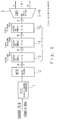
- Figure 4 is a block diagram of a first form of this invention.
- the first form of this invention has a plurality of identifier comparator units 22 respectively comprise one of comparing means 21 and a corresponding one of input identifier storing means 20.
- the identifier comparator units 22 comprising the input identifier storing means 20 and the comparing means 21 are assumed to be provided in correspondence with the total number of combinations of identifiers (VPIs and VCIs) attached to incoming ATM cells, e.g. inputted from subscribers to the switcher via its input highways.
- a controlling means 19 controls the storage of these identifiers in the input identifier storing means 20.
- the combination of a VPI and a VCI forms a total of up to twenty-eight (28) bits.
- the total number of such combinations is far less and is considered to be in the order of 28, i.e. two hundred fifty-six (256).
- this invention assumes there are two hundred fifty-six (256) combinations of identifiers and that the identifier comparator units 22 comprising the input identifier storing means 20 and the comparing means 21 are provided respectively in a total of two hundred fifty-six (256).
- the corresponding input identifier storing means 20 in one (1) of the identifier comparator units 22 stores the VPI and VCI attached to the header part of an incoming ATM cell on an input highway received from an order taker/server in response to an instruction by a call processor, which are in a controlling means 19.
- the corresponding one of the comparing means 21 in the same one of the identifier comparator units 22 compares the VPI and VCI attached to the header part of the incoming ATM cell actually inputted from an input highway with the content of the input identifier storing means 20 for a match.
- the input identifier storing means 20 in the corresponding identifier comparator units 22 store different combinations of input identifiers (VPIs/VCIs). When any of these combinations matches the identifiers attached to the header part of an incoming ATM cell actually received from an input highway, only the particular one of the comparing means 21 outputs a comparison result indicating a match.
- the input identifier storing means 20 in the identifier comparator units 22 store the contents of the identifiers in the header part of all incoming ATM cells from input highways. Each of the identifier comparator units 22 has a different memory content.
- the comparing means 21 in all the identifier comparator units 22 receive the content of the VPI and VCI taken from an incoming ATM cell actually received. As a result, one of the two hundred fifty-six (256) identifier comparator units 22 outputs a match signal showing that the comparison result is a match.
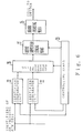
- Figure 5 is block diagram of a second form of this invention.
- Output identifier storing means 23 and output controllers 24 are provided respectively for the identifier comparator units 22. Also a header inserting means 25 is provided.
- the output identifier storing means 23 stores the memory contents of the input identifier storing means 20, i.e. the VPIs and VCIs to be attached to the header part of outgoing ATM cells on output highways and tags giving information about switching ATM cells in the switcher received from an order taker/server in a controlling means 26.
- the input identifier storing means 20 respectively in the identifier comparator units 22 store different combinations of input identifiers (VPIs/VCIs).
- the output controlling means 24 When any of the comparing means 21 in the identifier comparator units 22 detect a match between the contents of one of the input identifier storing means 20 and the identifiers attached to the header part of an incoming ATM cell actually received from an input highway, the output controlling means 24 has the particular one of the comparing means 21 output the content of the corresponding one of the output identifier storing means 23.
- the header inserting means 25 inserts this content into the header part of the incoming ATM cell actually received from an input highway, and supplies it to the switcher.
- the corresponding one of the output controllers 24 forwards the match signal outputted from one of the comparing means 21 in the corresponding one of the two hundred fifty-six (256) identifier comparator units 22 causes the corresponding one of the output controllers 24 to output the memory content in the corresponding one of the output identification storing means 23 to the header inserting means 25.
- the header inserting means 25 inserts the memory content in the header part of the incoming ATM cell on its way to the switcher.
- the output identifier storing means 23 are provided for the respective ones of the two hundred fifty-six (256) identifier comparator units 22, and the memory contents in the input identifier storing means 20 correspond one-to-one to those in the output identifier storing means 23.
- Figure 6 is a block diagram of a third form of this invention.
- the third form of this invention utilizes an output identification storing means 27, an address specifying means 28 and a header inserting means 25.
- the output identifier storing means 27 e.g. comprising a random access memory, stores VPIs and VCIs, e.g. corresponding to two-hundred fifty-six (256) addresses, to be attached to the header part of outgoing ATM cells on output highways and also stores the tags giving information for routing ATM cells in the switcher.
- the address specifying means 28 specifies an address in the output identifier storing means 27 in response to a receipt of an output from one of the comparing means 21 in the corresponding one of the identifier comparator units 22, which are provided in correspondence with the total number of combinations of VPIs and VCIs, e.g. two hundred fifty-six (256) combinations.
- the address is specified e.g. by converting 1 through 256, respectively for the two hundred fifty-six (256) identifier comparator units 22, from decimal numbers to binary numbers to be used as read addresses for accessing the output identifier storing means 27.
- the output identifier storing means 27 outputs the memory content specified by a read address to the header inserting means 25, which inserts this content into the header part of the incoming ATM cell on its way to the switcher.
- the address specifying means 28 receives all the outputs from the two hundred fifty-six (256) comparators 22. When one of the comparing means 21 in the corresponding one of the two hundred fifty-six (256) comparators 22 outputs a match signal, the address specifying means 28 specifies the read address for accessing the output identification storing means 27.
- the header inserter inserts the VPI and VCI to be attached to an outgoing ATM cell on an output highway as well as the tag giving information for routing the incoming ATM cell in the switcher, which are read from the output identifier storing means 27 by the read address, in the header part of the incoming ATM cell on its way to the switcher.
- this invention enables all twenty-eight (28) bits of the VPI and VCI attached to the header part of an incoming ATM cell to be fully supported.
- This invention physically provides e.g. two hundred fifty-six (256) identifier comparators for comparing the VPI and VCI of an incoming ATM cell with their memory contents. Because respective comparators individually compare the VPI and VCI in a maximum of twenty-eight (28) bits with their memory contents, this invention enables the VPI and VCI of an incoming ATM cell to be converted to those of an outgoing ATM cell, no matter where in the twenty-eight (28) bits the two hundred fifty-six (256) identifier combinations reside, as described later.
- 256 two hundred fifty-six
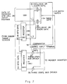
- Figure 7 is a block diagram of an embodiment of a virtual identifier conversion system.
- a first register 30 corresponds to the input identifier storing means 20 shown in Figure 4 and stores all possible VPIs and VCIs attached to incoming ATM cells on input highways.
- a second register 31 corresponds to the output identifier storing means 23 shown in Figure 5 and stores a total of forty-four (44) bits comprising all combinations of a VPI and a VCI in a maximum of twenty-eight (28) bits to be attached to the header part of outgoing ATM cells in a one-to-one correspondence with the memory content in the first register 30, as well as tags in sixteen (16) bits.
- a comparator 32 comprises twenty-eight (28) EXOR gates 33 and a NAND gate 34 for receiving their outputs.
- the twenty-eight (28) EXOR gates 33 receive the stored contents in the first register 30 in negative logic and the VPI/VCI data attached to the header part of incoming ATM cells on input highways in positive logic, both in one (1) bit units.
- the NAND circuit 34 output an "L" level signal, which is supplied to a control input terminal of three state bus drivers 35 to put it in an "ON" state. This causes the three state bus drivers 35 to output identifiers and a tag in a total of forty-four (44) bits stored in the second register 31 to a header inserter, described later.
- FIG 8 is a block diagram of a first embodiment of a virtual channel converter (VCC).
- VCC virtual channel converter
- a third register 37 receives data of the VPI and VCI of an incoming ATM cell transmitted from an input highway, at a timing controlled by a timing generator 36.
- the number of conversion circuit modules 38 each comprising the first and second registers 30 and 31, the comparator 32 and three state bus drivers 35, is the same as the number of combinations of the VPI and VCI. That is, there are two hundred fifty-six (256) conversion circuit modules 38, for example.
- the comparator 32 compares the contents of the third register 37 with that of the first register 30 in each of the conversion circuit modules 38. Only when the contents in the first and third registers 30 and 37 completely match, the comparator 32 outputs a signal to the three state bus drivers 35 for turning its gate on.
- the header inserter 10 attaches, to the header part of an incoming ATM cell on its way to the multiplexer 2 shown in Figure 1, the contents of the second register 31, i.e. the VPI and VCI to be attached to the header part of an outgoing ATM cell on an output highway for the switcher and the tag for routing the incoming ATM cell in the switcher in a total of forty-four (44) bits.
- FIG. 9 is a block diagram of a second embodiment of a virtual channel converter (VCC).
- VCC virtual channel converter
- Each of the conversion circuit modules 39 comprises only the first register 30 and the comparator 32.
- An encoder 40, a selector 41 and a random access memory (RAM) 42 are provided, in lieu of the second register 31 and the three state bus drivers 35.
- the random access memory (RAM) 42 stores a total of forty-four (44) bits comprising the VPI and VCI to be attached to an ATM cell on an output highway and a tag for routing an incoming ATM cell in a switcher.
- the RAM 42 pre-stores contents comprising forty-four (44) bits to be outputted to the header inserter 10 at a write address inputted from the selector 41 under control of the order taker/server 8.
- the encoder 40 converts the decimal integer between 1 and 256, the number of an output line of the comparator 32, to a binary number to be supplied through the selector 41 to the RAM 42 as its read address.
- the header inserter 10 attaches the forty-four (44) bit data in the read address to an ATM cell on its way to the multiplexer 2.
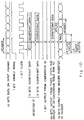
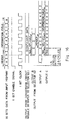
- FIG 10 is a timing chart for a virtual channel converter (VCC) in the first and second embodiments shown in Figures 8 and 9.
- VCC virtual channel converter
- the third register 37 receives data of an incoming ATM cell on an input highway in sixteen (16) bit units, in synchronization with a clock cycle, starting at a rise of an enable signal from the timing generator 36 to an "H".
- the third register 37 also receives the clock signal frequency e.g. at nine mega hertz (9MHz), from an input highway. Because the VPI and VCI in the header part of an ATM has a maximum of twenty-eight (28) bits, the third register 37 receives sixteen (16) bits in synchronization with a first clock cycle and twelve (12) bits in synchronization with a second clock cycle. After the third register 37 stores significant data comprising twenty-eight (28) bits, one of the comparators 32 outputs a match signal upon detecting a match. This causes the bus drivers 35 or the RAM 42 to output significant data comprising forty-four (44) bits to the header inserter 10.
- the header inserter 10 outputs a tag comprising sixteen (16) bits after one and a half (1.5) clock cycles after a rise of the enable signal to an "H" and the VPI and VCI after a further elapse of one (1) clock cycle.
- the header inserter 10 attaches those forty-four (44) bits to the ATM cell on its way to the multiplexer 2. The operation of the header inserter 10 will be further explained later.
- the format of an ATM cell shown in Figure 11 is assumed to be slightly different from that of one shown in Figure 2. That is, data on an input highway shown at the top in Figure 11 comprise thirty-two (32) bits [or four (4) bytes] of a header part, whereas data outputted from the header inserter 10 shown at the bottom in Figure 11 comprise forty-eight (48) bits [or six (6) bytes] of a header part. This is because the header part of an ATM cell in a virtual channel converter and a switcher has a format different from that shown in Figure 2.
- FIG 11 shows an ATM cell format for use in an ATM cell switcher.
- the head end of the header part of an ATM cell stores two (2) bytes of a tag for routing the ATM cell into the switcher. Then, following the head end, the header part of an ATM cell stores four (4) bytes of the VPI and VCI.
- One (1) byte for the header error control (HEC) included in the header part of an ATM cell format shown in Figure 2 is unnecessary for routing the ATM cell in the switcher. Because the virtual channel converter changes VPI and VCI and takes off one (1) byte for HEC, before an ATM cell is inputted to a switcher, the output side of the switcher attaches one (1) byte for a new HEC and deletes the tag, thus making the header part again five (5) bytes before the ATM cell outgoes on an output highway.
- HEC header error control
- FIG 12 is a block diagram of the timing generator 36 shown in Figures 8 and 9.
- the timing generator 36 comprises a shift register 50, three (3) inverters 51, 52 and 53, and two (2) AND circuits 54 and 55.
- the shift register 50 receives the enable signal illustrated in Figure 10 at its data input terminal.
- Inverter 51 inverts a clock signal inputted together with data from an input highway and supplies the inverted clock signal to a clock input terminal of the shift register 50.
- Two (2) inverters 52 and 53 are connected respectively to output terminals 1 and 2 of the shift register 50.
- AND circuit 54 receives an output of the shift register 50 from its output terminal 0 and an output from inverter 52.
- AND circuit 55 receives an output of the shift register 50 from its output terminal 1 and an output from inverter 53.
- Figure 13 is a timing chart for the timing generator 36.
- the shift register 50 receives an inverted signal [1] of a clock signal at its clock input terminal and an enable signal [2] of a clock signal at its data input terminal, and outputs three (3) results of sequentially shifting the enable signal [2] as shifted signals [3], [4] and [5] from its output terminals 0, 1 and 2 at rises of the inverted signal [1] received at its clock input terminal.
- AND circuit 54 produces signal A, as the logical product of shifted signal [3] and the inversion of shifted signal [4] obtained by inverter 52.
- Signal A is used as a timing for storing, in the third register 37, the first sixteen (16) of the twenty-eight (28) bits of VPI and VCI.
- AND circuit 55 produces signal B as the logical product of shifted signal [4] and the inversion of shifted signal [5] obtained by inverter 52.
- Signal B is used as a timing for storing, in the third register 37, the remaining twelve (12) bits in the twenty-eight (28) bits of VPI and VCI.
- the third register 37 comprises e.g. a first register element for storing sixteen (16) bits and a second register element for storing twelve (12) bits and uses signal A as a timing for storing sixteen (16) bit data in the first register element and signal B as a timing for storing twelve (12) bit data in the second register element.
- FIG 14 is a block diagram of the order taker/server 8 shown in Figures 8 and 9.
- the order taker/server 8 comprises an order taking register 58 and an expander 59, for example.
- the order taking register 58 outputs twenty-eight (28) bits to the first register 30 for storing the VPI and VCI attached to the header part of an incoming ATM cell on an input highway and forty-four (44) bits to the second register 31 for storing the VPI and VCI to be attached to the header part of the outgoing ATM cell on an output highway and a tag for routing the ATM cell in the switcher.
- the expander 59 supplies set pulses to the first and second registers 30 and 31 through the order taking register 58 from the call processor (CPR) 7.
- CPR call processor
- FIG 15 is a block diagram of the header inserter 10 shown in Figures 8 and 9.
- the header inserter 10 has a delayer 61 and a first selector 62 and a second selector 63.
- the delayer 61 delays the information field of an ATM cell by two and a half (2.5) clock cycles, as shown in Figure 10.
- the first selector 62 sequentially outputs the tag, VPI and VCI outputted from the conversion circuit modules 38 shown in Figure 8.
- the second selector 63 sequentially outputs the output from the first selector 62 and the delayer 61.
- Figure 16 is a timing chart for the header inserter 10.
- the conversion circuit modules 38 output significant data delayed by one and a half (1.5) clock cycles.
- the first selector 62 receives the delayed significant data, and the second selector 63 sequentially outputs the tag, VPI and VCI as output B.
- the second selector 63 sequentially outputs, as output C, output B from the first selector 62 and output A from the delayer 61, to the multiplexer 2 shown in Figure 1.
- the data a and b in the header part are converted to data a' and b'.
- this invention enables the VPI and VCI in a maximum total of twenty-eight (28) bits to be fully supported, thereby structuring an almighty virtual channel converter.
- This invention is applicable to a communications system using ATM cells such as a B-ISDN.
- An increase in the number of conversion circuit modules allows a greater number of identifier combinations.
- Putting the conversion circuit modules in LSIs contributes to the improved effectiveness of an ISDN switcher.
Landscapes
- Engineering & Computer Science (AREA)
- Computer Networks & Wireless Communication (AREA)
- Signal Processing (AREA)
- Data Exchanges In Wide-Area Networks (AREA)
Claims (20)
- Système de conversion d'identifieur virtuel (1) placé dans un étage précédant un commutateur (2, 6) en vue d'une utilisation dans un réseau numérique à intégration de services large bande pour convertir un identifieur de voie virtuelle (VPI) et un identifieur de canal virtuel (VCI) liés à une cellule ATM sur une autoroute d'entrée dudit commutateur selon un identifieur de voie virtuelle et un identifieur de canal virtuel à lier à ladite cellule ATM sur une autoroute de sortie et pour lier une étiquette pour aiguiller ladite cellule ATM dans ledit commutateur, ledit système de conversion d'identifieur virtuel étant caractérisé en ce qu'il comprend :une pluralité d'unités de comparateur d'identifieur (22) dont chacune comprend un moyen de stockage d'identifieur d'entrée (20) pour stocker une combinaison possible de l'un desdits identifieurs de voie virtuelle et de l'un desdits identifieurs de canal virtuel liés à la partie d'en-tête de ladite cellule ATM sur ladite autoroute d'entrée et un moyen de comparaison (21) pour comparer en vue d'une correspondance ledit identifieur de voie virtuelle et ledit identifieur de canal virtuel liés à ladite cellule ATM entrée depuis ladite autoroute d'entrée au contenu stocké dans ledit moyen de stockage d'identifieur d'entrée ; etun moyen de commande (19) pour stocker toutes les combinaisons d'un identifieur de voie virtuelle et d'un identifieur de canal virtuel pouvant être liés à une cellule ATM entrée sur ledit commutateur selon une base biunivoque, dans l'un approprié desdits moyens de stockage d'identifieur d'entrée respectivement dans ladite pluralité d'unités de comparateur d'identifieur.
- Système de conversion d'identifieur virtuel selon la revendication 1, dans lequel :ledit moyen de stockage d'identifieur d'entrée comprend un premier registre (30) pour bloquer ledit identifieur de voie virtuelle et ledit identifieur de canal virtuel ;ledit moyen de comparaison comprend des portes OU-exclusif (33) dont chacune reçoit le contenu du bit correspondant stocké dans ledit premier registre selon une logique négative au niveau de leurs premières bornes d'entrée et de chaque bit dudit identifieur de voie virtuelle et dudit identifieur de canal virtuel liés à une cellule ATM entrée depuis ladite autoroute d'entrée au niveau de leurs secondes bornes d'entrée, lesdites portes OU-exclusif étant prévues selon un nombre égal au nombre total de bits composant ledit identifieur de voie virtuelle et ledit identifieur de canal virtuel ;ledit moyen de comparaison comprend en outre une porte NON-ET (34) pour recevoir toutes les sorties provenant desdites portes OU-exclusif ;ledit moyen de commande comprend un processeur d'appel (7) pour commander la commutation de ladite cellule ATM et un serveur/preneur d'ordre (8) pour avoir ledit premier registre qui bloque les valeurs de l'identifieur de voie virtuelle et de l'identifieur de canal virtuel liés à une cellule ATM entrée depuis une autoroute d'entrée sous la commande dudit processeur d'appel.
- Système de conversion d'identifieur virtuel selon la revendication 1, dans lequel chacune de ladite pluralité d'unités de comparateur d'identifieur comprend en outre :un moyen de stockage d'identifieur de sortie (23) commandé par ledit moyen de commande, ledit moyen de stockage d'identifieur de sortie étant prévu pour stocker un identifieur de voie virtuelle et un identifieur de canal virtuel à lier à une cellule ATM sur une autoroute de sortie ainsi qu'une étiquette permettant d'aiguiller ladite cellule ATM dans ledit commutateur ;un moyen de commande de sortie (24) pour émettre en sortie le contenu dudit moyen de stockage d'identifieur de sortie lorsque ledit moyen de comparaison détecte une correspondance ; etun moyen d'insertion d'en-tête (25) pour insérer le contenu de l'un desdits moyens de stockage d'identifieur de sortie dans la partie d'en-tête de ladite cellule ATM sur son chemin jusqu'audit commutateur, ledit un desdits moyens de stockage d'identifieur de sortie inclus dans l'une desdites unités de comparateur d'identifieur ayant l'un desdits moyens de comparaison qui détecte une correspondance.
- Système de conversion d'identifieur virtuel selon la revendication 2, dans lequel chacune de ladite pluralité d'unités de comparateur d'identifieur comprend en outre :un moyen de stockage d'identifieur de sortie commandé par ledit moyen de commande, ledit moyen de stockage d'identifieur de sortie permettant de stocker un identifieur de voie virtuelle et un identifieur de canal virtuel à lier à une cellule ATM sur une autoroute de sortie ainsi qu'une étiquette permettant d'aiguiller ladite cellule ATM dans ledit commutateur ;un moyen de commande de sortie pour émettre en sortie le contenu dudit moyen de stockage d'identifieur de sortie lorsque ledit moyen de comparaison détecte une correspondance ; etun moyen d'insertion d'en-tête pour insérer le contenu de l'un desdits moyens de stockage d'identifieur de sortie dans la partie d'en-tête de ladite cellule ATM sur son chemin jusqu'audit commutateur, ledit un desdits moyens de stockage d'identifieur de sortie inclus dans l'une desdites unités de comparateur d'identifieur ayant l'un desdits moyens de comparaison qui détecte une correspondance.
- Système de conversion d'identifieur virtuel selon la revendication 3, dans lequel :chacun de ladite pluralité de moyens de stockage d'identifieur de sortie comprend un second registre pour bloquer ledit identifieur de voie virtuelle, ledit identifieur de canal virtuel et ladite étiquette permettant d'aiguiller ladite cellule ATM dans le commutateur ;chacun desdits moyens de commande de sortie comprend des dispositifs de commande de bus à trois états (35) pour recevoir les données de bits respectifs bloquées dans ledit second registre, le nombre desdits dispositifs de commande de bus à trois états étant égal au nombre total de bits dans ledit identifieur de voie virtuelle, ledit identifieur de canal virtuel et ladite étiquette entrés sur une borne d'entrée de commande recevant un signal de correspondance provenant de l'un desdits moyens de comparaison ; etledit moyen d'insertion d'en-tête comprend un retardateur (61) pour retarder ladite cellule ATM entrée depuis ladite autoroute d'entrée de deux cycles et demi (2,5) d'un signal d'horloge, un premier sélecteur (62) pour émettre en sortie séquentiellement les données bloquées dans ledit second registre selon l'ordre constitué par une étiquette, un identifieur de voie virtuelle et un identifieur de canal virtuel, et un second sélecteur (63) pour émettre en sortie séquentiellement une sortie provenant dudit premier sélecteur et une sortie provenant dudit retardateur par commutation.
- Système de conversion d'identifieur virtuel selon la revendication 4, dans lequel :chacun de ladite pluralité de moyens de stockage d'identifieur de sortie comprend un second registre pour bloquer ledit identifieur de voie virtuelle, ledit identifieur de canal virtuel et ladite étiquette permettant d'aiguiller ladite cellule ATM dans le commutateur ;chacun desdits moyens de commande de sortie comprend des dispositifs de commande de bus à trois états pour recevoir les données de bits respectifs bloquées dans ledit second registre, le nombre desdits dispositifs de commande de bus à trois états étant égal au nombre total de bits dans ledit identifieur de voie virtuelle, ledit identifieur de canal virtuel et ladite étiquette entrés sur une borne d'entrée de commande recevant un signal de correspondance provenant de l'un desdits moyens de comparaison ; etledit moyen d'insertion d'en-tête comprend un retardateur pour retarder ladite cellule ATM entrée depuis ladite autoroute d'entrée de deux cycles et demi (2,5) d'un signal d'horloge, un premier sélecteur pour émettre en sortie séquentiellement les données bloquées dans ledit second registre selon l'ordre constitué par une étiquette, un identifieur de voie virtuelle et un identifieur de canal virtuel, et un second sélecteur pour émettre en sortie séquentiellement une sortie provenant dudit premier sélecteur et une sortie provenant dudit retardateur par commutation.
- Système de conversion d'identifieur virtuel selon la revendication 3, dans lequel ledit convertisseur de canal virtuel comprend en outre :un troisième registre pour bloquer -ledit identifieur de voie virtuelle et ledit identifieur de canal virtuel liés à ladite cellule ATM entrée depuis ladite autoroute d'entrée et pour émettre en sortie les données bloquées de bits respectifs dans ledit identifieur de voie virtuelle et dans ledit identifieur de canal virtuel sur lesdites secondes bornes d'entrée desdites portes OU-exclusif dans ledit moyen de comparaison ; etun générateur de cadencement pour générer un cadencement pour avoir ledit troisième registre qui bloque ledit identifieur de voie virtuelle et ledit identifieur de canal virtuel.
- Système de conversion d'identifieur virtuel selon la revendication 4, dans lequel ledit convertisseur de canal virtuel comprend en outre :un troisième registre (37) pour bloquer ledit identifieur de voie virtuelle et ledit identifieur de canal virtuel liés à ladite cellule ATM entrée depuis ladite autoroute d'entrée et pour émettre en sortie les données bloquées de bits respectifs dans ledit identifieur de voie virtuelle et dans ledit identifieur de canal virtuel sur ladite seconde borne d'entrée desdites portes OU-exclusif dans ledit moyen de comparaison ; etun générateur de cadencement (36) pour générer un cadencement pour avoir ledit troisième registre qui bloque ledit identifieur de voie virtuelle et ledit identifieur de canal virtuel.
- Système de conversion d'identifieur virtuel selon la revendication 5, dans lequel ledit convertisseur de canal virtuel comprend en outre :un troisième registre pour bloquer ledit identifieur de voie virtuelle et ledit identifieur de canal virtuel liés à ladite cellule ATM entrée depuis ladite autoroute d'entrée et pour émettre en sortie les données bloquées de bits respectifs dans ledit identifieur de voie virtuelle et dans ledit identifieur de canal virtuel sur lesdites secondes bornes d'entrée desdites portes OU-exclusif dans ledit moyen de comparaison ; etun générateur de cadencement pour générer un cadencement pour avoir ledit troisième registre qui bloque ledit identifieur de voie virtuelle et ledit identifieur de canal virtuel.
- Système de conversion d'identifieur virtuel selon la revendication 6, dans lequel ledit convertisseur de canal virtuel comprend en outre :un troisième registre pour bloquer ledit identifieur de voie virtuelle et ledit identifieur de canal virtuel liés à ladite cellule ATM entrée depuis ladite autoroute d'entrée et pour émettre en sortie les données bloquées de bits respectifs dans ledit identifieur de voie virtuelle et dans ledit identifieur de canal virtuel sur ladite seconde borne d'entrée desdites portes OU-exclusif dans ledit moyen de comparaison ; etun générateur de cadencement pour générer un cadencement pour avoir ledit troisième registre qui bloque ledit identifieur de voie virtuelle et ledit identifieur de canal virtuel.
- Système de conversion d'identifieur virtuel selon la revendication 1, comprenant en outre :un moyen de stockage d'identifieur de sortie (27) commandé par ledit moyen de commande pour stocker toutes lesdites combinaisons d'un identifieur de voie virtuelle, d'un identifieur de canal virtuel et d'une étiquette à lier à ladite cellule ATM sur ladite autoroute de sortie ;un moyen de spécification d'adresse (28) pour recevoir des sorties respectives provenant dudit moyen de comparaison, ledit moyen de spécification d'adresse permettant de spécifier une adresse dans ledit moyen de stockage d'identifieur de sortie ; etun moyen d'insertion d'en-tête (25) pour insérer les données de l'adresse dans ledit moyen de stockage d'identifieur de sortie dans la partie d'en-tête de ladite cellule ATM sur son chemin jusqu'audit commutateur, ladite adresse étant spécifiée par ledit moyen de spécification d'adresse, lesdites données correspondant au contenu dudit moyen de stockage d'identifieur d'entrée.
- Système de conversion d'identifieur virtuel selon la revendication 2, comprenant en outre :un moyen de stockage d'identifieur de sortie commandé par ledit moyen de commande pour stocker toutes lesdites combinaisons d'un identifieur de voie virtuelle, d'un identifieur de canal virtuel et d'une étiquette à lier à ladite cellule ATM sur ladite autoroute de sortie ;un moyen de spécification d'adresse pour recevoir des sorties respectives provenant dudit moyen de comparaison, ledit moyen de spécification d'adresse permettant de spécifier une adresse dans ledit moyen de stockage d'identifieur de sortie ; etun moyen d'insertion d'en-tête pour insérer les données de l'adresse dans ledit moyen de stockage d'identifieur de sortie dans la partie d'en-tête de ladite cellule ATM sur son chemin jusqu'audit commutateur, ladite adresse étant spécifiée par ledit moyen de spécification d'adresse, lesdites données correspondant au contenu dudit moyen de stockage d'identifieur d'entrée.
- Système de conversion d'identifieur virtuel selon la revendication 11, dans lequel :ledit moyen de stockage d'identifieur de sortie comprend une mémoire vive (42) pour stocker lesdites combinaisons d'un identifieur de voie virtuelle, d'un identifieur de canal virtuel et d'une étiquette ; etledit moyen de spécification d'adresse comprend un codeur (40) pour convertir des sorties provenant de moyens de comparaison respectifs dans ladite pluralité d'unités de comparateur d'identifieur pour lire des adresses dans ladite mémoire vive et un sélecteur (41) pour émettre en sortie, sur ladite mémoire vive, des adresses d'écriture appliquées par ledit moyen de commande lors d'une écriture de données et lesdites adresses de lecture appliquées par ledit codeur lors d'une lecture de données.
- Système de conversion d'identifieur virtuel selon la revendication 12, dans lequel :ledit moyen de stockage d'identifieur de sortie comprend une mémoire vive pour stocker lesdites combinaisons d'un identifieur de voie virtuelle, d'un identifieur de canal virtuel et d'une étiquette ; etledit moyen de spécification d'adresse comprend un codeur pour convertir des sorties provenant des moyens de comparaison respectifs dans ladite pluralité d'unités de comparateur d'identifieur pour lire des adresses dans ladite mémoire vive et un sélecteur pour émettre en sortie sur ladite mémoire vive des adresses d'écriture appliquées par ledit moyen de commande suite à une écriture de données et lesdites adresses de lecture appliquées par ledit codeur suite à une lecture de données.
- Système de conversion d'identifieur virtuel selon la revendication 11, dans lequel ledit convertisseur de canal virtuel comprend en outre :un troisième registre pour bloquer ledit identifieur de voie virtuelle et ledit identifieur de canal virtuel liés à ladite cellule ATM entrée depuis ladite autoroute d'entrée et pour émettre en sortie les données bloquées de bits respectifs dans ledit identifieur de voie virtuelle et dans ledit identifieur de canal virtuel sur lesdites secondes bornes d'entrée desdites portes OU-exclusif dans ledit moyen de comparaison ; etun générateur de cadencement pour générer un cadencement pour avoir ledit troisième registre qui bloque ledit identifieur de voie virtuelle et ledit identifieur de canal virtuel.
- Système de conversion d'identifieur virtuel selon la revendication 12, dans lequel ledit convertisseur de canal virtuel comprend en outre :un troisième registre pour bloquer ledit identifieur de voie virtuelle et ledit identifieur de canal virtuel liés à ladite cellule ATM entrée depuis ladite autoroute d'entrée et pour émettre en sortie les données bloquées de bits respectifs dans ledit identifieur de voie virtuelle et dans ledit identifieur de canal virtuel sur ladite seconde borne d'entrée desdites portes OU-exclusif dans ledit moyen de comparaison ; etun générateur de cadencement pour générer un cadencement pour avoir ledit troisième registre qui bloque ledit identifieur de voie virtuelle et ledit identifieur de canal virtuel.
- Système de conversion d'identifieur virtuel selon la revendication 13, dans lequel ledit convertisseur de canal virtuel comprend en outre :un troisième registre pour bloquer ledit identifieur de voie virtuelle et ledit identifieur de canal virtuel liés à ladite cellule ATM entrée depuis ladite autoroute d'entrée et pour émettre en sortie les données bloquées de bits respectifs dans ledit identifieur de voie virtuelle et dans ledit identifieur de canal virtuel sur lesdites secondes bornes d'entrée desdites portes OU-exclusif dans ledit moyen de comparaison ; etun générateur de cadencement pour générer un cadencement pour avoir ledit troisième registre qui bloque ledit identifieur de voie virtuelle et ledit identifieur de canal virtuel.
- Système de conversion d'identifieur virtuel selon la revendication 14, dans lequel ledit convertisseur de canal virtuel comprend en outre :un troisième registre pour bloquer ledit identifieur de voie virtuelle et ledit identifieur de canal virtuel liés à ladite cellule ATM entrée depuis ladite autoroute d'entrée et pour émettre en sortie les données bloquées de bits respectifs dans ledit identifieur de voie virtuelle et dans ledit identifieur de canal virtuel sur ladite seconde borne d'entrée desdites portes OU-exclusif dans ledit moyen de comparaison ; etun générateur de cadencement pour générer un cadencement pour avoir ledit troisième registre qui bloque ledit identifieur de voie virtuelle et ledit identifieur de canal virtuel.
- Système de conversion d'identifieur de canal virtuel selon la revendication 1, dans lequel :ledit identifieur de voie virtuelle et ledit identifieur de canal virtuel dans la partie d'en-tête de ladite cellule ATM comprennent vingt-quatre (24) bits au total lorsque ledit commutateur commute ledit ATM entre un utilisateur et un réseau ; etledit identifieur de voie virtuelle et ledit identifieur de canal virtuel dans la partie d'en-tête de ladite cellule ATM comprennent vingt-huit (28) bits au total lorsque ledit commutateur commute ladite cellule ATM entre un utilisateur et un réseau.
- Système de conversion d'identifieur de canal virtuel selon la revendication 1, dans lequel :
ledit convertisseur de canal virtuel élimine un (1) octet pour un contrôle d'erreur d'en-tête parmi les cinq (5) octets dans la partie d'en-tête de ladite cellule ATM provenant de ladite autoroute d'entrée et lie une étiquette pour aiguiller ladite cellule ATM dans ledit commutateur à ladite cellule ATM sur son chemin jusqu'audit commutateur pour ainsi faire en sorte que la partie d'en-tête soit égale à une somme de ladite étiquette et de quatre (4) octets.
Applications Claiming Priority (2)
| Application Number | Priority Date | Filing Date | Title |
|---|---|---|---|
| JP28260590A JP3001953B2 (ja) | 1990-10-20 | 1990-10-20 | 仮想識別子変換装置 |
| JP282605/90 | 1990-10-20 |
Publications (2)
| Publication Number | Publication Date |
|---|---|
| EP0482550A1 EP0482550A1 (fr) | 1992-04-29 |
| EP0482550B1 true EP0482550B1 (fr) | 1996-03-20 |
Family
ID=17654684
Family Applications (1)
| Application Number | Title | Priority Date | Filing Date |
|---|---|---|---|
| EP91117916A Expired - Lifetime EP0482550B1 (fr) | 1990-10-20 | 1991-10-21 | Système de conversion d'identificateur virtuel |
Country Status (5)
| Country | Link |
|---|---|
| US (1) | US5271010A (fr) |
| EP (1) | EP0482550B1 (fr) |
| JP (1) | JP3001953B2 (fr) |
| CA (1) | CA2053840C (fr) |
| DE (1) | DE69118095T2 (fr) |
Families Citing this family (76)
| Publication number | Priority date | Publication date | Assignee | Title |
|---|---|---|---|---|
| JP3262142B2 (ja) * | 1992-01-16 | 2002-03-04 | 富士通株式会社 | Atmセル化装置、atmセル化方法、ノード、及びノードにおける多重化方法 |
| DE4230743C2 (de) * | 1992-09-14 | 1994-03-17 | Siemens Ag | Verfahren zum Rundsenden von Zellen in einer im Asynchron-Transfer-Modus wirkenden Koppelstruktur eines Kommunikationssystems |
| SE515274C2 (sv) * | 1992-11-09 | 2001-07-09 | Ericsson Telefon Ab L M | Paketväljare för telekommunikationsanläggning |
| SE470544B (sv) * | 1992-11-24 | 1994-07-25 | Ellemtel Utvecklings Ab | För en bitfelsövervakning i en väljarutrustning avsedd anordning |
| GB9300279D0 (en) * | 1993-01-08 | 1993-03-03 | Plessey Telecomm | Telecommunications network |
| JPH0744545B2 (ja) * | 1993-01-21 | 1995-05-15 | 日本電気株式会社 | Atmセル分解/組立てシステム |
| DE4323471C2 (de) * | 1993-07-14 | 1996-10-17 | Atecom Advanced Telecommunicat | Anordnung und Verfahren zum Bearbeiten von Datenstrukturen bei deren Durchlauf durch einen Netzwerkknoten |
| US5430715A (en) * | 1993-09-15 | 1995-07-04 | Stratacom, Inc. | Flexible destination address mapping mechanism in a cell switching communication controller |
| JP3167228B2 (ja) * | 1993-09-20 | 2001-05-21 | 富士通株式会社 | Vccテーブルのアクセス方法及びバーチャルチャネル変換装置 |
| DE4340329C2 (de) * | 1993-11-26 | 2002-06-20 | Tenovis Gmbh & Co Kg | Verfahren zur Erzeugung von Leitadressen für in einem nach dem asynchronen Transfermodus (ATM) arbeitenden Vermittlungssystem zu übertragende Pakete |
| US5467349A (en) * | 1993-12-21 | 1995-11-14 | Trw Inc. | Address handler for an asynchronous transfer mode switch |
| US5504743A (en) * | 1993-12-23 | 1996-04-02 | British Telecommunications Public Limited Company | Message routing |
| DE69424315T2 (de) * | 1994-02-25 | 2000-11-30 | International Business Machines Corp., Armonk | Vorrichtung und verfahren zum abbilden von bits |
| US5493564A (en) * | 1994-03-25 | 1996-02-20 | Sprint International Communications Corp. | Method and apparatus for global routing of electronic messages |
| US5452301A (en) * | 1994-04-26 | 1995-09-19 | Klingman; Edwin E. | Data transmission and control system using local, externally generated D, Q, and M bits in X.25 packets |
| US5926482A (en) | 1994-05-05 | 1999-07-20 | Sprint Communications Co. L.P. | Telecommunications apparatus, system, and method with an enhanced signal transfer point |
| US6181703B1 (en) * | 1995-09-08 | 2001-01-30 | Sprint Communications Company L. P. | System for managing telecommunications |
| US6023474A (en) * | 1996-11-22 | 2000-02-08 | Sprint Communications C.O.L.P. | Broadband telecommunications system interface |
| US6631133B1 (en) * | 1994-05-05 | 2003-10-07 | Sprint Communications Company L.P. | Broadband telecommunications system |
| US6633561B2 (en) | 1994-05-05 | 2003-10-14 | Sprint Communications Company, L.P. | Method, system and apparatus for telecommunications control |
| US6031840A (en) * | 1995-12-07 | 2000-02-29 | Sprint Communications Co. L.P. | Telecommunications system |
| US6314103B1 (en) | 1994-05-05 | 2001-11-06 | Sprint Communications Company, L.P. | System and method for allocating bandwidth for a call |
| US6430195B1 (en) | 1994-05-05 | 2002-08-06 | Sprint Communications Company L.P. | Broadband telecommunications system interface |
| US5991301A (en) * | 1994-05-05 | 1999-11-23 | Sprint Communications Co. L.P. | Broadband telecommunications system |
| BR9507610A (pt) | 1994-05-05 | 1997-08-19 | Sprint Communications Co | Método sistema e aparelho para o controle das telecomunicações |
| US6172977B1 (en) * | 1994-05-05 | 2001-01-09 | Sprint Communications Company, L. P. | ATM direct access line system |
| US5920562A (en) | 1996-11-22 | 1999-07-06 | Sprint Communications Co. L.P. | Systems and methods for providing enhanced services for telecommunication call |
| US5703876A (en) * | 1994-05-05 | 1997-12-30 | Christie; Joseph Michael | ATM transport system |
| JP3356875B2 (ja) | 1994-05-23 | 2002-12-16 | 沖電気工業株式会社 | 有効チャネル識別回路 |
| US5414701A (en) * | 1994-07-22 | 1995-05-09 | Motorola, Inc. | Method and data structure for performing address compression in an asynchronous transfer mode (ATM) system |
| US5530806A (en) * | 1994-12-15 | 1996-06-25 | At&T Corp. | Method and apparatus for storing and retrieving routing information in a network node |
| KR0132959B1 (ko) * | 1994-12-22 | 1998-04-21 | 양승택 | 비동기 전달모드(atm)망에서 비연결형 데이터 서비스 제공을 위한 비연결형 서버 |
| US5627836A (en) * | 1995-01-31 | 1997-05-06 | Bell Atlantic Network Services, Inc. | VPI/VCI administration |
| US5815737A (en) * | 1995-06-05 | 1998-09-29 | Pmc-Sierra, Inc. | Approach for identifying a subset of asynchronous transfer mode (ATM) VPI/VCI values in the complete VPI/VCI range |
| US5734865A (en) * | 1995-06-07 | 1998-03-31 | Bull Hn Information Systems Inc. | Virtual local area network well-known port routing mechanism for mult--emulators in an open system environment |
| US5636371A (en) * | 1995-06-07 | 1997-06-03 | Bull Hn Information Systems Inc. | Virtual network mechanism to access well known port application programs running on a single host system |
| US5909427A (en) * | 1995-07-19 | 1999-06-01 | Fujitsu Network Communications, Inc. | Redundant switch system and method of operation |
| US5719864A (en) * | 1995-08-11 | 1998-02-17 | International Business Machines Corp. | Logical channel resolution in asynchronous transmission mode communication systems |
| US5898671A (en) * | 1995-09-14 | 1999-04-27 | Fujitsu Network Communications, Inc. | Transmitter controlled flow control for buffer allocation in wide area ATM networks |
| US6081529A (en) * | 1995-11-22 | 2000-06-27 | Sprint Communications Company, L. P. | ATM transport system |
| JP2000517488A (ja) * | 1996-01-16 | 2000-12-26 | フジツウ ネットワーク コミュニケーションズ,インコーポレイテッド | Atm網用の信頼性と柔軟性のあるマルチキャスト機構 |
| AU2257097A (en) * | 1996-02-02 | 1997-08-22 | Sprint Communications Company, L.P. | Atm gateway system |
| US5898830A (en) * | 1996-10-17 | 1999-04-27 | Network Engineering Software | Firewall providing enhanced network security and user transparency |
| US5826014A (en) | 1996-02-06 | 1998-10-20 | Network Engineering Software | Firewall system for protecting network elements connected to a public network |
| US5870550A (en) * | 1996-02-26 | 1999-02-09 | Network Engineering Software | Web server employing multi-homed, moldular framework |
| US8117298B1 (en) | 1996-02-26 | 2012-02-14 | Graphon Corporation | Multi-homed web server |
| US5757796A (en) * | 1996-04-26 | 1998-05-26 | Cascade Communications Corp. | ATM address translation method and apparatus |
| US5940393A (en) * | 1996-05-28 | 1999-08-17 | Sprint Communications Co. L.P. | Telecommunications system with a connection processing system |
| US5835730A (en) * | 1996-07-31 | 1998-11-10 | General Instrument Corporation Of Delaware | MPEG packet header compression for television modems |
| US5748905A (en) * | 1996-08-30 | 1998-05-05 | Fujitsu Network Communications, Inc. | Frame classification using classification keys |
| US6667982B2 (en) | 1996-11-22 | 2003-12-23 | Sprint Communications Company, L.P. | Broadband telecommunications system interface |
| EP0932971B1 (fr) | 1996-11-22 | 2005-10-05 | Sprint Communications Company, L.P. | Systeme et procede de transport d'un appel dans un reseau de telecommunication |
| US6115380A (en) * | 1996-11-22 | 2000-09-05 | Sprint Communications Co., L.P. | Broadband telecommunications system |
| US6014378A (en) * | 1996-11-22 | 2000-01-11 | Sprint Communications Company, L.P. | Telecommunications tandem system for circuit-based traffic |
| US6002689A (en) * | 1996-11-22 | 1999-12-14 | Sprint Communications Co. L.P. | System and method for interfacing a local communication device |
| US5867499A (en) * | 1996-12-31 | 1999-02-02 | Northern Telecom Limited | ATM switch having location independent virtual-connection switches |
| JP3579208B2 (ja) * | 1997-03-11 | 2004-10-20 | 株式会社東芝 | ノード装置及びメッセージ交換方法 |
| US6067299A (en) * | 1997-04-16 | 2000-05-23 | Sprint Communications Company, L.P. | Communications system for providing ATM connections and echo cancellation |
| US6137800A (en) * | 1997-05-09 | 2000-10-24 | Sprint Communications Company, L. P. | System and method for connecting a call |
| US6704327B1 (en) | 1997-05-09 | 2004-03-09 | Sprint Communications Company, L.P. | System and method for connecting a call |
| US6178170B1 (en) | 1997-05-13 | 2001-01-23 | Sprint Communications Company, L. P. | System and method for transporting a call |
| US6963570B1 (en) * | 1997-07-15 | 2005-11-08 | Comsat Corporation | Method and apparatus for adaptive loss-less compression of cell/packet headers |
| US6700890B1 (en) * | 1997-12-22 | 2004-03-02 | Cisco Technology, Inc. | Method and apparatus for configuring permanent virtual connection (PVC) information stored on network devices in an ATM network logically configured with subnetworks |
| US6810040B1 (en) | 1997-12-22 | 2004-10-26 | Cisco Technology, Inc. | Method and apparatus for configuring network devices |
| US6483837B1 (en) | 1998-02-20 | 2002-11-19 | Sprint Communications Company L.P. | System and method for connecting a call with an interworking system |
| US6563918B1 (en) | 1998-02-20 | 2003-05-13 | Sprint Communications Company, LP | Telecommunications system architecture for connecting a call |
| JPH11275082A (ja) * | 1998-03-19 | 1999-10-08 | Fujitsu Ltd | マルチライン対応のセルヘッダー変換装置及びその方法 |
| US6452939B1 (en) * | 1998-03-24 | 2002-09-17 | Samsung Electronics Co., Ltd. | ATM interface device with double header conversion |
| US6160871A (en) | 1998-04-10 | 2000-12-12 | Sprint Communications Company, L.P. | Communications test system |
| JP2000031962A (ja) | 1998-07-10 | 2000-01-28 | Fujitsu Ltd | Isdnバックアップチャネルの有効利用方式 |
| US6714217B2 (en) | 1998-12-18 | 2004-03-30 | Sprint Communication Company, L.P. | System and method for providing a graphical user interface to, for building, and/or for monitoring a telecommunication network |
| US7079530B1 (en) | 1999-02-25 | 2006-07-18 | Sprint Communications Company L.P. | System and method for caching toll free number information |
| US7103068B1 (en) | 1999-05-04 | 2006-09-05 | Sprint Communication Company L.P. | System and method for configuring bandwidth transmission rates for call connections |
| US6895088B1 (en) | 1999-05-21 | 2005-05-17 | Sprint Communications Company L.P. | System and method for controlling a call processing system |
| US6704314B1 (en) | 1999-12-15 | 2004-03-09 | Sprint Communications Company, L.P. | Method and apparatus to control cell substitution |
| US7434128B2 (en) * | 2005-03-24 | 2008-10-07 | Hewlett-Packard Development Company, L.P. | Systems and methods for identifying system links |
Family Cites Families (4)
| Publication number | Priority date | Publication date | Assignee | Title |
|---|---|---|---|---|
| GB8428533D0 (en) * | 1984-11-12 | 1984-12-19 | Secr Defence | Data decoder |
| AU604444B2 (en) * | 1987-11-11 | 1990-12-13 | Nec Corporation | Frame relay type data switching apparatus |
| NL8801120A (nl) * | 1988-04-29 | 1989-11-16 | At & T & Philips Telecomm | Kruispuntschakelaar voor het doorschakelen van pakketten. |
| JPH03104451A (ja) * | 1989-09-19 | 1991-05-01 | Fujitsu Ltd | 多段リンク交換システムのルート切替え方式 |
-
1990
- 1990-10-20 JP JP28260590A patent/JP3001953B2/ja not_active Expired - Lifetime
-
1991
- 1991-10-21 US US07/780,108 patent/US5271010A/en not_active Expired - Lifetime
- 1991-10-21 DE DE69118095T patent/DE69118095T2/de not_active Expired - Lifetime
- 1991-10-21 CA CA002053840A patent/CA2053840C/fr not_active Expired - Fee Related
- 1991-10-21 EP EP91117916A patent/EP0482550B1/fr not_active Expired - Lifetime
Also Published As
| Publication number | Publication date |
|---|---|
| JP3001953B2 (ja) | 2000-01-24 |
| CA2053840C (fr) | 1995-03-14 |
| DE69118095T2 (de) | 1996-09-05 |
| EP0482550A1 (fr) | 1992-04-29 |
| US5271010A (en) | 1993-12-14 |
| JPH04157845A (ja) | 1992-05-29 |
| DE69118095D1 (de) | 1996-04-25 |
Similar Documents
| Publication | Publication Date | Title |
|---|---|---|
| US5271010A (en) | Virtual identifier conversion system | |
| US5214639A (en) | Communication switching element and method for transmitting variable length cells | |
| US5577037A (en) | Method of processing inclusively STM signals and ATM signals and switching system employing the same | |
| US6289011B1 (en) | 2n×n multiplexing switch | |
| US6356557B1 (en) | Hot insertable UTOPIA interface with automatic protection switching for backplane applications | |
| CA2034841A1 (fr) | Systeme de commutation a mode de transfert asynchrone de tranches de bits | |
| US6724760B2 (en) | ATM switch | |
| US5369635A (en) | High bit rate cell switching element in CMOS technology | |
| EP0674409B1 (fr) | Dispositif pour tester des canaux ATM | |
| US5459743A (en) | Address decision system having address check system | |
| US6628659B1 (en) | ATM cell switching system | |
| JPH1098483A (ja) | Atm交換機とそのipcセル伝送方法 | |
| US3997728A (en) | Unit for the simultaneous switching of digital information and signalling data in P.C.M. transmission systems | |
| JP3244665B2 (ja) | Tone及びDTMF発生機能を備えたATMセル変換装置及びその方法 | |
| JPH11261601A (ja) | 交換システムのatmセル変換装置及びその方法 | |
| JPH07336354A (ja) | Stmデータ/atmセル変換方法及び装置 | |
| JP3455379B2 (ja) | 速度変換回路 | |
| US4482995A (en) | Time division multiplex switching network unit | |
| CA2063516C (fr) | Methode de diffusion par commutateur d'autoacheminement | |
| Eng et al. | Advances in shared-memory designs for gigabit ATM switching | |
| KR0159671B1 (ko) | 공유메모리 구조를 갖는 출력 버퍼형 스위치 | |
| KR100261733B1 (ko) | Atm 교환기의 니블 클록 펄스 분주회로 및 그 방법 | |
| KR100272568B1 (ko) | 사설 교환기의 셀 스위칭 장치 및 방법 | |
| KR100206191B1 (ko) | 셀지연 우선순위를 이용한 라우터 | |
| KR0138596B1 (ko) | 소용량 전전자 교환기의 중계선 정합장치 |
Legal Events
| Date | Code | Title | Description |
|---|---|---|---|
| PUAI | Public reference made under article 153(3) epc to a published international application that has entered the european phase |
Free format text: ORIGINAL CODE: 0009012 |
|
| AK | Designated contracting states |
Kind code of ref document: A1 Designated state(s): DE FR GB |
|
| 17P | Request for examination filed |
Effective date: 19920730 |
|
| 17Q | First examination report despatched |
Effective date: 19950109 |
|
| GRAA | (expected) grant |
Free format text: ORIGINAL CODE: 0009210 |
|
| AK | Designated contracting states |
Kind code of ref document: B1 Designated state(s): DE FR GB |
|
| REF | Corresponds to: |
Ref document number: 69118095 Country of ref document: DE Date of ref document: 19960425 |
|
| ET | Fr: translation filed | ||
| PLBE | No opposition filed within time limit |
Free format text: ORIGINAL CODE: 0009261 |
|
| STAA | Information on the status of an ep patent application or granted ep patent |
Free format text: STATUS: NO OPPOSITION FILED WITHIN TIME LIMIT |
|
| 26N | No opposition filed | ||
| REG | Reference to a national code |
Ref country code: GB Ref legal event code: IF02 |
|
| REG | Reference to a national code |
Ref country code: GB Ref legal event code: 732E |
|
| REG | Reference to a national code |
Ref country code: FR Ref legal event code: TP |
|
| PGFP | Annual fee paid to national office [announced via postgrant information from national office to epo] |
Ref country code: FR Payment date: 20101004 Year of fee payment: 20 |
|
| PGFP | Annual fee paid to national office [announced via postgrant information from national office to epo] |
Ref country code: GB Payment date: 20100923 Year of fee payment: 20 |
|
| PGFP | Annual fee paid to national office [announced via postgrant information from national office to epo] |
Ref country code: DE Payment date: 20101029 Year of fee payment: 20 |
|
| REG | Reference to a national code |
Ref country code: DE Ref legal event code: R071 Ref document number: 69118095 Country of ref document: DE |
|
| REG | Reference to a national code |
Ref country code: DE Ref legal event code: R071 Ref document number: 69118095 Country of ref document: DE |
|
| REG | Reference to a national code |
Ref country code: GB Ref legal event code: PE20 Expiry date: 20111020 |
|
| PG25 | Lapsed in a contracting state [announced via postgrant information from national office to epo] |
Ref country code: GB Free format text: LAPSE BECAUSE OF EXPIRATION OF PROTECTION Effective date: 20111020 |
|
| PG25 | Lapsed in a contracting state [announced via postgrant information from national office to epo] |
Ref country code: DE Free format text: LAPSE BECAUSE OF EXPIRATION OF PROTECTION Effective date: 20111022 |