EP0482648B1 - Méthode de croissance d'un cristal semiconducteur - Google Patents
Méthode de croissance d'un cristal semiconducteur Download PDFInfo
- Publication number
- EP0482648B1 EP0482648B1 EP91118176A EP91118176A EP0482648B1 EP 0482648 B1 EP0482648 B1 EP 0482648B1 EP 91118176 A EP91118176 A EP 91118176A EP 91118176 A EP91118176 A EP 91118176A EP 0482648 B1 EP0482648 B1 EP 0482648B1
- Authority
- EP
- European Patent Office
- Prior art keywords
- substrate
- gas
- reaction gas
- blow tube
- tube
- Prior art date
- Legal status (The legal status is an assumption and is not a legal conclusion. Google has not performed a legal analysis and makes no representation as to the accuracy of the status listed.)
- Expired - Lifetime
Links
- 239000013078 crystal Substances 0.000 title claims description 78
- 239000004065 semiconductor Substances 0.000 title claims description 55
- 238000000034 method Methods 0.000 title claims description 50
- 239000000758 substrate Substances 0.000 claims description 155
- 239000012495 reaction gas Substances 0.000 claims description 97
- 239000007789 gas Substances 0.000 claims description 89
- QGZKDVFQNNGYKY-UHFFFAOYSA-N Ammonia Chemical compound N QGZKDVFQNNGYKY-UHFFFAOYSA-N 0.000 claims description 27
- 238000003825 pressing Methods 0.000 claims description 27
- XCZXGTMEAKBVPV-UHFFFAOYSA-N trimethylgallium Chemical compound C[Ga](C)C XCZXGTMEAKBVPV-UHFFFAOYSA-N 0.000 claims description 20
- JLTRXTDYQLMHGR-UHFFFAOYSA-N trimethylaluminium Chemical compound C[Al](C)C JLTRXTDYQLMHGR-UHFFFAOYSA-N 0.000 claims description 11
- 229910052751 metal Inorganic materials 0.000 claims description 10
- 239000002184 metal Substances 0.000 claims description 10
- IBEFSUTVZWZJEL-UHFFFAOYSA-N trimethylindium Chemical compound C[In](C)C IBEFSUTVZWZJEL-UHFFFAOYSA-N 0.000 claims description 8
- 238000005229 chemical vapour deposition Methods 0.000 claims description 7
- RBFQJDQYXXHULB-UHFFFAOYSA-N arsane Chemical compound [AsH3] RBFQJDQYXXHULB-UHFFFAOYSA-N 0.000 claims description 6
- HQWPLXHWEZZGKY-UHFFFAOYSA-N diethylzinc Chemical compound CC[Zn]CC HQWPLXHWEZZGKY-UHFFFAOYSA-N 0.000 claims description 6
- 238000010438 heat treatment Methods 0.000 claims description 6
- VNWKTOKETHGBQD-UHFFFAOYSA-N methane Chemical compound C VNWKTOKETHGBQD-UHFFFAOYSA-N 0.000 claims description 6
- 229910021529 ammonia Inorganic materials 0.000 claims description 5
- 229910000069 nitrogen hydride Inorganic materials 0.000 claims description 5
- BLRPTPMANUNPDV-UHFFFAOYSA-N Silane Chemical compound [SiH4] BLRPTPMANUNPDV-UHFFFAOYSA-N 0.000 claims description 4
- 229910000070 arsenic hydride Inorganic materials 0.000 claims description 3
- RWSOTUBLDIXVET-UHFFFAOYSA-N Dihydrogen sulfide Chemical compound S RWSOTUBLDIXVET-UHFFFAOYSA-N 0.000 claims description 2
- XYFCBTPGUUZFHI-UHFFFAOYSA-N Phosphine Chemical compound P XYFCBTPGUUZFHI-UHFFFAOYSA-N 0.000 claims description 2
- 229910052734 helium Inorganic materials 0.000 claims description 2
- SPVXKVOXSXTJOY-UHFFFAOYSA-N selane Chemical compound [SeH2] SPVXKVOXSXTJOY-UHFFFAOYSA-N 0.000 claims description 2
- 229910000058 selane Inorganic materials 0.000 claims description 2
- 229910000077 silane Inorganic materials 0.000 claims description 2
- JMASRVWKEDWRBT-UHFFFAOYSA-N Gallium nitride Chemical group [Ga]#N JMASRVWKEDWRBT-UHFFFAOYSA-N 0.000 claims 1
- 239000010408 film Substances 0.000 description 57
- 229910052594 sapphire Inorganic materials 0.000 description 34
- 239000010980 sapphire Substances 0.000 description 34
- UFHFLCQGNIYNRP-UHFFFAOYSA-N Hydrogen Chemical compound [H][H] UFHFLCQGNIYNRP-UHFFFAOYSA-N 0.000 description 27
- IJGRMHOSHXDMSA-UHFFFAOYSA-N Atomic nitrogen Chemical compound N#N IJGRMHOSHXDMSA-UHFFFAOYSA-N 0.000 description 18
- 238000006243 chemical reaction Methods 0.000 description 16
- OKTJSMMVPCPJKN-UHFFFAOYSA-N Carbon Chemical compound [C] OKTJSMMVPCPJKN-UHFFFAOYSA-N 0.000 description 10
- 229910052799 carbon Inorganic materials 0.000 description 10
- 230000003247 decreasing effect Effects 0.000 description 10
- 239000001257 hydrogen Substances 0.000 description 9
- 229910052739 hydrogen Inorganic materials 0.000 description 9
- 229910052757 nitrogen Inorganic materials 0.000 description 9
- 229910001218 Gallium arsenide Inorganic materials 0.000 description 7
- 238000007664 blowing Methods 0.000 description 6
- 238000002488 metal-organic chemical vapour deposition Methods 0.000 description 6
- 230000005855 radiation Effects 0.000 description 6
- 239000011261 inert gas Substances 0.000 description 5
- 238000005259 measurement Methods 0.000 description 5
- 239000000203 mixture Substances 0.000 description 5
- VYPSYNLAJGMNEJ-UHFFFAOYSA-N silicon dioxide Inorganic materials O=[Si]=O VYPSYNLAJGMNEJ-UHFFFAOYSA-N 0.000 description 5
- 238000011109 contamination Methods 0.000 description 4
- 238000007796 conventional method Methods 0.000 description 4
- 238000004020 luminiscence type Methods 0.000 description 4
- 239000010453 quartz Substances 0.000 description 4
- 239000000969 carrier Substances 0.000 description 3
- 230000000694 effects Effects 0.000 description 3
- 230000006698 induction Effects 0.000 description 3
- QSHDDOUJBYECFT-UHFFFAOYSA-N mercury Chemical compound [Hg] QSHDDOUJBYECFT-UHFFFAOYSA-N 0.000 description 3
- 229910052753 mercury Inorganic materials 0.000 description 3
- 230000003287 optical effect Effects 0.000 description 3
- 239000000047 product Substances 0.000 description 3
- 239000010935 stainless steel Substances 0.000 description 3
- 229910001220 stainless steel Inorganic materials 0.000 description 3
- 239000012159 carrier gas Substances 0.000 description 2
- 238000000354 decomposition reaction Methods 0.000 description 2
- 239000007788 liquid Substances 0.000 description 2
- 239000000463 material Substances 0.000 description 2
- 229910017464 nitrogen compound Inorganic materials 0.000 description 2
- 150000002830 nitrogen compounds Chemical class 0.000 description 2
- 239000000126 substance Substances 0.000 description 2
- 239000012808 vapor phase Substances 0.000 description 2
- 108091006149 Electron carriers Proteins 0.000 description 1
- XUIMIQQOPSSXEZ-UHFFFAOYSA-N Silicon Chemical compound [Si] XUIMIQQOPSSXEZ-UHFFFAOYSA-N 0.000 description 1
- 229910052782 aluminium Inorganic materials 0.000 description 1
- 230000002238 attenuated effect Effects 0.000 description 1
- 239000007795 chemical reaction product Substances 0.000 description 1
- 238000004140 cleaning Methods 0.000 description 1
- 239000011248 coating agent Substances 0.000 description 1
- 238000000576 coating method Methods 0.000 description 1
- 230000007547 defect Effects 0.000 description 1
- 230000001419 dependent effect Effects 0.000 description 1
- 238000000151 deposition Methods 0.000 description 1
- 230000008021 deposition Effects 0.000 description 1
- 238000009826 distribution Methods 0.000 description 1
- 239000001307 helium Substances 0.000 description 1
- SWQJXJOGLNCZEY-UHFFFAOYSA-N helium atom Chemical compound [He] SWQJXJOGLNCZEY-UHFFFAOYSA-N 0.000 description 1
- 150000002431 hydrogen Chemical class 0.000 description 1
- 239000012535 impurity Substances 0.000 description 1
- 229910052738 indium Inorganic materials 0.000 description 1
- 238000004519 manufacturing process Methods 0.000 description 1
- 229910001092 metal group alloy Inorganic materials 0.000 description 1
- 229910001507 metal halide Inorganic materials 0.000 description 1
- 150000005309 metal halides Chemical class 0.000 description 1
- 238000001451 molecular beam epitaxy Methods 0.000 description 1
- 238000000465 moulding Methods 0.000 description 1
- 230000010355 oscillation Effects 0.000 description 1
- 238000006552 photochemical reaction Methods 0.000 description 1
- 238000005424 photoluminescence Methods 0.000 description 1
- 238000005268 plasma chemical vapour deposition Methods 0.000 description 1
- 239000011347 resin Substances 0.000 description 1
- 229920005989 resin Polymers 0.000 description 1
- 230000000630 rising effect Effects 0.000 description 1
- 229910052710 silicon Inorganic materials 0.000 description 1
- 239000010703 silicon Substances 0.000 description 1
- HBMJWWWQQXIZIP-UHFFFAOYSA-N silicon carbide Chemical compound [Si+]#[C-] HBMJWWWQQXIZIP-UHFFFAOYSA-N 0.000 description 1
- 229910010271 silicon carbide Inorganic materials 0.000 description 1
- 239000010409 thin film Substances 0.000 description 1
- 229910052724 xenon Inorganic materials 0.000 description 1
- FHNFHKCVQCLJFQ-UHFFFAOYSA-N xenon atom Chemical compound [Xe] FHNFHKCVQCLJFQ-UHFFFAOYSA-N 0.000 description 1
Images


Classifications
-
- C—CHEMISTRY; METALLURGY
- C30—CRYSTAL GROWTH
- C30B—SINGLE-CRYSTAL GROWTH; UNIDIRECTIONAL SOLIDIFICATION OF EUTECTIC MATERIAL OR UNIDIRECTIONAL DEMIXING OF EUTECTOID MATERIAL; REFINING BY ZONE-MELTING OF MATERIAL; PRODUCTION OF A HOMOGENEOUS POLYCRYSTALLINE MATERIAL WITH DEFINED STRUCTURE; SINGLE CRYSTALS OR HOMOGENEOUS POLYCRYSTALLINE MATERIAL WITH DEFINED STRUCTURE; AFTER-TREATMENT OF SINGLE CRYSTALS OR A HOMOGENEOUS POLYCRYSTALLINE MATERIAL WITH DEFINED STRUCTURE; APPARATUS THEREFOR
- C30B25/00—Single-crystal growth by chemical reaction of reactive gases, e.g. chemical vapour-deposition growth
- C30B25/02—Epitaxial-layer growth
- C30B25/14—Feed and outlet means for the gases; Modifying the flow of the reactive gases
-
- C—CHEMISTRY; METALLURGY
- C30—CRYSTAL GROWTH
- C30B—SINGLE-CRYSTAL GROWTH; UNIDIRECTIONAL SOLIDIFICATION OF EUTECTIC MATERIAL OR UNIDIRECTIONAL DEMIXING OF EUTECTOID MATERIAL; REFINING BY ZONE-MELTING OF MATERIAL; PRODUCTION OF A HOMOGENEOUS POLYCRYSTALLINE MATERIAL WITH DEFINED STRUCTURE; SINGLE CRYSTALS OR HOMOGENEOUS POLYCRYSTALLINE MATERIAL WITH DEFINED STRUCTURE; AFTER-TREATMENT OF SINGLE CRYSTALS OR A HOMOGENEOUS POLYCRYSTALLINE MATERIAL WITH DEFINED STRUCTURE; APPARATUS THEREFOR
- C30B29/00—Single crystals or homogeneous polycrystalline material with defined structure characterised by the material or by their shape
- C30B29/10—Inorganic compounds or compositions
- C30B29/40—AIIIBV compounds wherein A is B, Al, Ga, In or Tl and B is N, P, As, Sb or Bi
- C30B29/403—AIII-nitrides
- C30B29/406—Gallium nitride
-
- C—CHEMISTRY; METALLURGY
- C30—CRYSTAL GROWTH
- C30B—SINGLE-CRYSTAL GROWTH; UNIDIRECTIONAL SOLIDIFICATION OF EUTECTIC MATERIAL OR UNIDIRECTIONAL DEMIXING OF EUTECTOID MATERIAL; REFINING BY ZONE-MELTING OF MATERIAL; PRODUCTION OF A HOMOGENEOUS POLYCRYSTALLINE MATERIAL WITH DEFINED STRUCTURE; SINGLE CRYSTALS OR HOMOGENEOUS POLYCRYSTALLINE MATERIAL WITH DEFINED STRUCTURE; AFTER-TREATMENT OF SINGLE CRYSTALS OR A HOMOGENEOUS POLYCRYSTALLINE MATERIAL WITH DEFINED STRUCTURE; APPARATUS THEREFOR
- C30B29/00—Single crystals or homogeneous polycrystalline material with defined structure characterised by the material or by their shape
- C30B29/10—Inorganic compounds or compositions
- C30B29/40—AIIIBV compounds wherein A is B, Al, Ga, In or Tl and B is N, P, As, Sb or Bi
- C30B29/42—Gallium arsenide
Definitions
- the present invention relates to a method of growing in vapor phase a semiconductor crystal film consisting of a nitrogen compound and, more particularly, to a method of vapor-growing a semiconductor crystal film by blowing a reaction gas on the surface of a substrate.
- Figs. 1 to 4 the example of Fig. 4 is known from Appl, Phys. Lett. 48 (1986)353).
- reaction gases are blown to a portion above and very close to the substrate 1 from a thin reaction gas blow tube 2 having an inner diameter of about 5 mm to 10 mm.
- the reaction gases are blown against the substrate as a high-speed flow at a flow rate of 2 m/sec or more.
- a GaN film having a thickness of about 2 to 5 ⁇ m can be grown on the sapphire substrate in a growth time of 30 to 60 minutes.
- Fig. 2 shows a conventional semiconductor crystal film growth apparatus.
- this apparatus comprises a chamber, a carbon susceptor 43 which is non-rotating and incorporated in the chamber and on which a substrate can be set obliquely to the horizontal direction, a reaction gas blow tube 45 capable of horizontally blowing a reaction gas to the substrate, and a reduction gas H 2 blow tube 44.
- a RF coil 42 is horizontally arranged and wound around the outer circumferential wall of the chamber around the carbon susceptor 43.
- a load-lock chamber 41 is connected to the chamber.
- a rotary pump 46 is connected to the chamber, and a turbo pump 47 and a rotary pump 48 are connected to the load-lock chamber 41.
- a reaction gas is horizontally blown to a substrate set obliquely to the horizontal direction on the fixed carbon susceptor. Note that the carbon susceptor is not rotated and no pressing gas is used.
- Fig. 3 shows an apparatus almost similar to the apparatus shown in Fig. 1.
- This apparatus comprises a chamber 51, a rotary carbon susceptor 53 incorporated in the chamber 51, a reaction gas blow tube 55 extending downward from the upper portion of the chamber 51, and a reduction gas H 2 blow tube 54.
- a vertically RF coil 52 is arranged and wound around the outer circumferential wall of the chamber 51 around the carbon susceptor 53.
- Fig. 4 shows an apparatus comprising a chamber 61, a rotary carbon susceptor 63 which is incorporated in the chamber 61 and on which a substrate can be set obliquely to the vertical direction, and a reaction gas blow tube 65 extending downward from the upper portion of the chamber 61.
- the reaction gas blow tube 65 is branched into lines 70 and 71 at its upper portion.
- a gas mixture of NH 3 and H 2 is flowed through the line 70, and a gas mixture of TMG and H 2 is flowed through the line 71.
- a vertically RF coil 62 is arranged and wound around the outer circumferential wall of the chamber 61 around the susceptor 63.
- the flow rate of a reaction gas In order to grow a semiconductor crystal film on a substrate by the above method, the flow rate of a reaction gas must be increased. That is, no GaN can be grown unless the flow rate of a reaction gas is 2 m/sec or more. This is assumed to be attributed to the fact that if the flow rate of a reaction gas is not sufficiently high, the reaction gas is prevented from reaching the substrate by a large heat convection current formed by a high reaction temperature.
- a thin reaction gas blow tube having an inner diameter of 5 to 10 mm is used in conventional growth methods.
- the lower opening end of this thin reaction gas blow tube is located at a position separated from above the surface of a substrate by 5 to 10 mm.
- the diameter of an area of the grown semiconductor crystal film is about 5 to 10 mm, i.e., only a very small film can be obtained.
- the area of a grown semiconductor crystal film is about 2/50 or less the area of the substrate, resulting in very low yield. That is, the conventional growth methods cannot uniformly grow a semiconductor crystal film in a large area having a diameter of 10 mm or more on the surface of a substrate.
- a large amount of a GaN reaction product adheres on the distal end of the thin reaction gas blow tube each time a semiconductor crystal film is grown on the surface of a substrate. If the temperature of the substrate is increased during the growth of the semiconductor crystal film, GaN deposited on the reaction gas blow tube is decomposed into Ga metal by the influence of this heat, and the Ga metal falls on the substrate during the reaction. Since no GaN is grown on portions where Ga fell, the growth yield is extremely decreased.
- the thin reaction gas blow tube must be replaced by a new one or washed each time the reaction is caused, resulting in very poor operability.
- a CVD method such as a metal organic chemical vapor deposition method (to be referred to as an MOCVD method hereinafter) or a molecular beam epitaxy method is used to grow semiconductor crystals on a substrate set in a reactor
- MOCVD method metal organic chemical vapor deposition method
- a molecular beam epitaxy method is used to grow semiconductor crystals on a substrate set in a reactor.
- this "monitor window” is used to externally observe the crystal growth state, or light is radiated on a crystal layer through the “monitor window” to give optical energy to the growing crystal layer, thereby changing the growth state.
- FIG. 5 shows a conventional apparatus using an example of the "monitor window”.
- This reactor vessel 10 has a double cylinder structure using quartz tubes.
- An induction coil 12 for heating a substrate 18 is wound outside an outer tube.
- a "monitor window” 13 is open in an inner tube at a position above the substrate 18.
- a reaction gas is supplied into the inner tube to grow a semiconductor crystal layer on the surface of a substrate.
- Hydrogen for example, is flowed into the outer tube to prevent the reaction gas from flowing into the outer tube.
- the entire reactor must be replaced after it is used only several times.
- complicated steps of, e.g., vacuum baking or gas baking must be repeatedly performed a number of times over several days in order to remove the moisture, resulting in a very cumbersome operation.
- a method of growing a semiconductor crystal layer As a method of growing a semiconductor crystal layer, a method of growing crystals while radiating light is available. In this method, a growth temperature can be significantly decreased by radiating light, and a light source is arranged outside a reactor in order to radiate light. The light source radiates an epitaxial crystal layer with light which is transmitted through a "monitor window". In this method, it is very important to keep the "monitor window" clean because a contaminated "monitor window” absorbs light to reduce light radiation intensity on the epitaxial crystal layer.
- EP-A-0254654 discloses a method for a chemical vapor deposition of a metallic thin film on e.g. a heated silicon substrate by using metal halides as reaction gases. The deposition is performed so as to form metal films and metal alloy films and the reaction gas is provided in a laminar flow near and parallel to the surface of the substrate. An inert gas injecting plate is disposed in a direction perpendicular to the substrate to limit the reaction to the space near the substrate.
- EP-A-0328417 discloses an apparatus for forming crystals under a reduced pressure and a revolving laminar gas flow by utilizing a photochemical reaction. JP-A-62-228478 teaches an apparatus for chemical vapor deposition which works under a reduced pressure and in which the diameter of the reaction gas supply means is increased toward the tip.
- the present invention has been made to solve the above conventional problems.
- a method of vapor-growing in vapor phase a semiconductor crystal layer comprising in particular the steps of supplying a reaction gas to a portion above a surface of a heated substrate so as to be parallel or obliquely to the substrate, and blowing a pressing gas, which is inert with respect to the reaction gas, toward the substrate to bring the reaction gas into contact with the surface of the substrate.
- the pressing gas is preferably blown using a blow tube which is widened like a funnel toward a blow port. More preferably, this blow tube is transparent.
- an apparatus for growing a semiconductor crystal film comprising a reactor, a susceptor, provided in the reactor, for supporting a substrate, means for heating the susceptor, reaction gas supply means for supplying a reaction gas parallel or obliquely to the substrate, and a blow tube, having a shape widened toward a blow port thereof like a funnel, for blowing a pressing gas, which is inert with respect to the reaction gas, toward the substrate to bring the reaction gas into contact with a surface of the substrate.
- this blow tube is transparent.
- the reaction gas blow tube need not to be arranged above a substrate. Therefore, even when GaN deposited on the reaction gas blow tube is decomposed into Ga metal, the Ga metal does not fall to adhere on the substrate. In addition, since the direction of the reaction gas is changed by the pressing gas, the Ga metal hardly reaches a substrate even when the reaction gas is blown parallel to the substrate. Therefore, the yield of a sapphire substrate is not decreased, and the reaction gas blow tube need not be frequently washed or replaced.
- this pressing gas The most important effect of this pressing gas is to urge and bring the reaction gas flowing parallel or obliquely to a substrate in contact with the surface of the substrate. If no pressing gas is used, almost no film growth is obtained on the substrate. The reason for this is that heat convection is caused on the substrate due to a high substrate temperature of about 1,000°C. If no pressing gas is used, the reaction gas is raised by the heat convection and cannot be brought into contact with the substrate. Therefore, the pressing gas is flowed to urge the rising reaction gas downward to be brought into contact with the substrate. As described above, in the method of the present invention, a GaN epitaxial film can be grown by using the pressing gas.
- the method of the present invention enables growth of GaN even when a reaction gas is horizontally blown. Furthermore, since a substrate is rotated, a GaN epitaxial film can be uniformly grown on a large area.
- the diameter of an effective area of a semiconductor crystal film grown on the surface of a substrate by one growth operation cycle is at most 10 mm. Therefore, when a sapphire substrate having a diameter of 50.8mm (2 inches) is used, this operation must be repeated a number of times making it difficult to form an uniform semiconductor crystal film on the entire substrate. On the contrary, when a semiconductor crystal film is grown on the surface of a sapphire substrate in accordance with the present invention, uniform GaN can be grown on the entire sapphire substrate even when the outer diameter of the substrate is 50.8mm (2 inches).
- a reaction gas is blown parallel or obliquely to a substrate, and a pressing gas is flowed toward the substrate, thereby forming a semiconductor crystal film.
- This method can be applied to materials which can be grown by chemical vapor deposition methods such as an MOCVD method, a plasma CVD method, and a microwave CVD method.
- Fig. 6 is a view schematically showing a method of growing a semiconductor crystal film according to the present invention. As shown in Fig. 6, a reaction gas is blown parallel or obliquely to a substrate 21 placed on a susceptor 24, and a pressing gas is blown toward the substrate 21, thereby changing the direction of a flow of the reaction gas to be blown against the substrate 21.
- the reaction gas is blown parallel to the substrate at a high speed, and the pressing gas is flowed vertically toward the substrate, thereby changing the direction of the reaction gas above the substrate so as to be blown against the substrate.
- reaction gas examples include metal organic gases such as trimethylgallium (TMG), trimethylaluminum (TMA), diethylzinc (DEZ), and trimethylindium (TMI), arsine (AsH 3 ), phosphine (PH 3 ), ammonia (NH 3 ), silane (SiH 4 ), H 2 Se, H 2 S, and methane (CH 4 ).
- TMG trimethylgallium
- TMA trimethylaluminum
- DEZ diethylzinc
- TMI trimethylindium
- ammonia NH 3
- silane SiH 4
- H 2 Se H 2 Se
- H 2 S and methane
- the pressing gas to be flowed vertically downward to a substrate is used to change the direction of the reaction gas toward the substrate, all inert gases having no influence on the reaction gas can be used as the pressing gas.
- the inert gas are H 2 gas, N 2 gas, He gas, Ne gas, and Ar gas, and these gases can be used singly or as a mixture thereof.
- a blow tube molded into a funnel-like shape widened toward a gas blow port is preferably used.
- a flow of the pressing gas forms a laminar flow which can uniformly flow toward a substrate.
- the size of the blow port is substantially the same as the substrate.
- a preferable flow rate of the pressing gas is 0.02 to 0.5 m/sec on the substrate.
- a crystal film can be uniformly grown on the entire surface of a sapphire substrate (C face) having a diameter of 50.8mm (2 inches), i.e., a large semiconductor crystal film can be grown by performing a vapor-growth operation once, great industrial merits can be obtained.
- the carrier concentration of a semiconductor crystal film manufactured by the method of the present invention is 1/10 or less than that of conventional products, and its Hall mobility is five or more times those thereof. Therefore, high-quality GaN can be grown.
- reaction gas blow tube for flowing the reaction gas can be arranged beside the susceptor, the temperature of the tube hardly rises, and almost no GaN adheres on the tube. Therefore, Ga melt does not fall on the substrate during the reaction to reduce the yield.
- the apparatus of the present invention comprises a reactor, a susceptor provided in the reactor, for supporting a substrate, means for heating the susceptor, reaction gas supply means for supplying a reaction gas parallel or obliquely to the substrate, and a blow tube, having a shape widened toward a blow port thereof like a funnel, for blowing a pressing gas, which is inert with respect to the reaction gas, toward the substrate to bring the reaction gas into contact with a surface of the substrate.
- the funnel-like portion of the blow tube is widened by an angle of preferably 20° or less, and more preferably, 10° or less with respect to the axis of the blow tube.
- the blow tube is preferably transparent.
- This apparatus may further comprise means for performing light radiation.
- the transparent tube is not contaminated by the reaction gas over a very long time period but functions as a "monitor window", a growth state of a semiconductor crystal layer can be accurately observed.
- the apparatus of the present invention using a transparent tube almost no contamination was found in the transparent tube even after the apparatus was used over several hundreds hours.
- the temperature of a substrate on which a crystal layer is grown can be measured through the transparent tube by detecting an infrared intensity radiated from the crystal layer, thereby measuring the film thickness of the crystal layer.
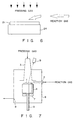
- the semiconductor crystal film vapor-growth apparatus shown in Fig. 7 is an apparatus for growing an epitaxial film consisting of GaN, AlN, InN, or mixed crystals thereof using an MOCVD method.
- the apparatus comprises a chamber 6, a susceptor 4, a heater 7, a reaction gas blow tube 2, and a sub blow tube 3.
- the susceptor 4 arranged in the chamber 6 has a horizontal upper surface and can rotate in a horizontal plane.
- the susceptor 4 is a circular column having a diameter of 30 to 100 mm and a height of 10 to 30 mm, and a shaft 5 is vertically fixed to the center of the lower surface of the susceptor 4.
- the susceptor 4 is heated up to 1,000°C or more by the heater 7 arranged below its lower surface.
- the susceptor 4 consists of a substance having a heat resistance and not contaminating gases in the chamber 6 upon heating, e.g., a material obtained by coating the surface of carbon with silicon carbide.
- the heater 7 is arranged close to but not in contact with the lower surface of the susceptor 4 and sets the susceptor 4 at a predetermined temperature in accordance with a temperature sensor (not shown) incorporated in the susceptor and ON/OFF control or supply current control.
- the heater 7 can be arranged in any position where it can heat the susceptor 4. Although not shown, the heater may be incorporated in the susceptor to form an integral structure.
- the reaction gas blow tube 2 is airtightly fixed through the chamber 6 horizontally or slightly obliquely.
- the distal end of the reaction gas blow tube 2 is extended close to the substrate 1 so as to blow a reaction gas on the surface of the substrate 1 placed on the susceptor 4.
- the reaction gas blow tube 2 blows hydrogen gas, ammonia gas, and trimethylgallium (TMG) or trimethylaluminum (TMA) gas to the surface of the substrate 1.
- TMG trimethylgallium
- TMA trimethylaluminum
- the sub blow tube 3 is airtightly fixed through the upper wall of the chamber 6.
- the sub blow tube 3 vertically blows an inert gas consisting of hydrogen or nitrogen downward to the substrate 1.
- the sub blow tube 3 has a funnel-like shape in which an opening area is widened downward.
- the lower end opening portion of the sub blow tube 3 is designed to have substantially the same size as the substrate 1.
- the lower end of the sub blow tube 3 is open close to the upper surface of the substrate 1.
- An interval between the lower end of the sub blow tube 3 and the substrate 1 is adjusted to be preferably 5 mm to 50 cm, and more preferably, 10 mm to 30 cm.
- An apparatus shown in Fig. 8 has a structure in which a light source 89 is arranged above a transparent tube 15 as shown in Fig. 7.
- the light source 89 radiates light on a semiconductor crystal layer to grow the semiconductor crystal layer at a low temperature.
- the light source 89 is arranged above the transparent tube 15, and light radiated from the light source 89 is focused by a lens 80 or a reflecting mirror 81 and uniformly radiated on the surface of a semiconductor crystal layer laminated on the substrate.
- An ultraviolet lamp such as a mercury lamp or a xenon lamp is used as the light source.
- the power of a lamp used as the light source is 200 W to several kW.
- the obtained substrate was removed from the chamber 6, and the film thickness distribution of the substrate was measured by a Nomarski microscope. As a result, the film thickness of a semiconductor crystal film fell within the range of 4 ⁇ m ⁇ 10% on the entire surface, i.e., was very uniform.
- the carrier concentration indicating purity of GaN obtained in Example 2 was 1 ⁇ 10 18 /cm 3 , and its Hall mobility was 250 cm 2 /V ⁇ sec.
- the concentration of an impurity serving as carriers is low or the number of lattice defects serving as carriers is small.
- N (nitrogen) vacancies are sources of n-type carriers in GaN crystals, and that the electron carrier concentration is 2 ⁇ 10 19 /cm 3 and the Hall mobility is 50 cm 2 /V ⁇ sec. Therefore, since the value of Hall mobility of GaN obtained by the apparatus of the present invention is five times that of the general mobility, this GaN is excellent in crystallinity.
- the sub blow tube in the upper portion of the apparatus was not contaminated at all. In addition, even after the reaction was caused twice or more by the apparatus, no Ga metal adhered on the surface of a grown semiconductor crystal film.
- the flow rate of the hydrogen gas supplied from the sub blow tube 3 was 15l/min.
- the flow rates of the ammonia gas, the hydrogen gas, and the TMA gas blown from the reaction gas blow tube 2 were 5l/min, 1l/min, and 1 ⁇ 10 -5 mol/min, respectively.
- This state was maintained for 1 minute to vapor-grow an AlN buffer layer on the surface of the sapphire substrate 1.
- Example 2 After the growth, the substrate 1 was removed from the chamber 6 and observed by a Nomarski microscope. As a result, the semiconductor crystal film obtained in Example 2 was vapor-grown on the entire surface of the 50.8mm (2-inch) diameter sapphire substrate 1. The surface of the film was a mirror surface, and the film thickness was 5 ⁇ m ⁇ 10% on the entire surface of the 50.8mm (2-inch) diameter substrate 1.
- the carrier concentration of GaN was 1 ⁇ 10 17 cm 3 , and its hole mobility was 350 cm 2 /V ⁇ sec, i.e., the crystallinity of GaN was very good.
- the carrier concentration of GaN was 5 ⁇ 10 17 /cm 3 , and its Hall mobility was 250 cm 2 /V ⁇ sec. Note that as described in Appl. Phys. lett, 48, 1986, page 353, the crystallinity of GaN is significantly improved by forming an AlN buffer layer before GaN is vapor-grown.
- InGaN was vapor-grown on the surface of a sapphire substrate by the following steps.
- the flow rate of both of hydrogen and nitrogen gases blown from the sub blow tube 3 was 5l/min.
- the substrate 1 was removed from the chamber 6, and its film thickness was observed.
- InGaN having a film thickness of 2 ⁇ m ⁇ 10% was grown on the entire surface of the 50.8mm (2-inch) diameter substrate.
- the Hall measurement was almost impossible because the resistivity of the InGaN crystal was very high, the photoluminescence of InGaN was measured to evaluate its crystallinity. Since luminescence of 440 nm was difficult to confirm in the InGaN crystal at room temperature, the luminescence was measured by decreasing the temperature to that of liquid nitrogen or liquid helium. Generally, the better the crystallinity, the higher the temperature at which luminescence can be measured. According to the present invention, however, luminescence of 440 nm was observed at room temperature. This indicates that the crystallinity of the semiconductor crystal film obtained by the method of the present invention is very good.
- Crystal growth was performed following the same procedures as in Example 1 except that in the seventh step in Example 1, after a GaN layer was grown for 60 minutes, diethylzinc (DEZ) was flowed in addition to the TMG gas at 5.0 ⁇ 10 -5 mol/min to vapor-grow a Zn-doped GaN layer for six minutes.
- DEZ diethylzinc
- a wafer having a structure in which a 4- ⁇ m thick undoped GaN layer was formed on a sapphire substrate and a 0.4- ⁇ m thick Zn-doped GaN layer was laminated thereon was manufactured.
- This wafer was cut into a 0.5-mm ⁇ 0.5-mm square piece by a dicing saw, and Al and In electrodes were extracted from the Zn-doped GaN layer and the undoped GaN layer, respectively.
- the resultant square sample was placed on a lead frame and subjected to wire bonding, and resin molding was performed to manufacture a light-emitting diode.
- GaN was grown on the surface of a sapphire substrate by the following steps.
- the structure shown in Fig. 1 was used as a vapor-growth apparatus.
- the thin reaction gas blow tube 2 having an inner diameter of 8 mm was vertically fixed above the sapphire substrate 1 so as to be separated by 10 mm from the substrate 1.
- the flow rates of the ammonia gas and the hydrogen gas blown from the reaction gas blow tube were adjusted to be 5l/min and 1l/min, respectively, and this state was maintained until the temperature was stabilized.
- the structure shown in Fig. 7 was used as a vapor growth apparatus.
- Infrared radiation radiated from the epitaxial layer in the step 7 ⁇ were detected by a narrow optical band-pass narrow pyrometer 14 for measuring an infrared intensity of 0.96 ⁇ m.
- Fig. 10 shows the infrared intensity detected by the pyrometer 14, i.e., the temperature.
- the film thickness of the epitaxial layer can be calculated by measuring the period of the oscillation.
- laser light having a particular wavelength may be radiated to measure the film thickness on the basis of a change in intensity of the reflected laser light.
- a 500-W mercury lamp was used as the light source 89.
- Ultraviolet rays radiated from the mercury lamp were focused by a lens and radiated on the substrate 1.
- the substrate temperature was increased to about 400°C to 500°C by the heater 7 to grow GaAs in accordance with a light radiation MOCVD method.
- Hydrogen gas was constantly flowed through the transparent tube 15 at a flow rate of 10.0l/min from the beginning to the end of the reaction.
- a GaAs epitaxial layer could be grown for 60 minutes. During the growth, ultraviolet rays could be uniformly radiated since the transparent tube 15 was not contaminated.
- the transparent tube 15 was not contaminated. Therefore, ultraviolet rays could be efficiently radiated on a GaAs substrate through the transparent tube 15.
Landscapes
- Chemical & Material Sciences (AREA)
- Engineering & Computer Science (AREA)
- Crystallography & Structural Chemistry (AREA)
- Materials Engineering (AREA)
- Metallurgy (AREA)
- Organic Chemistry (AREA)
- Inorganic Chemistry (AREA)
- Chemical Kinetics & Catalysis (AREA)
- General Chemical & Material Sciences (AREA)
Claims (8)
- Procédé de croissance en phase vapeur d'une couche de cristal semi-conducteur du groupe nitrure de gallium utilisant un procédé de dépôt chimique organo-métallique en phase vapeur, comprenant les étapes consistant à :chauffer un substrat (1) à une température située entre 550 °C et 1 050 °C ; etdélivrer un gaz réactionnel sur le substrat (1), dans lequel : ledit gaz réactionnel est délivré à travers un moyen d'alimentation en gaz réactionnel (2) avec une direction parallèle ou à l'oblique par rapport à ladite surface du substrat chauffé (1) ;ledit gaz réactionnel est suffisamment pressé par un gaz sous pression qui est inerte par rapport audit gaz réactionnel, ledit gaz sous pression étant soufflé séparément dans une autre direction vers ledit substrat (1) de sorte que ledit gaz réactionnel est amené en contact avec la surface dudit substrat (1) pour faire croítre ladite couche ; et chacune desdites étapes est exécutée à la pression atmosphérique.
- Procédé selon la revendication 1, caractérisé en ce que ledit gaz est soufflé par un tube de soufflage (3) élargi vers son orifice de soufflage du type cheminée.
- Procédé selon la revendication 2, caractérisé en ce qu'une partie du type cheminée dudit tube de soufflage (3) est élargie selon un angle qui n'est pas supérieur à 20° par rapport à un axe dudit tube de soufflage (3).
- Procédé selon la revendication 2, caractérisé en ce qu'une partie du type cheminée dudit tube de soufflage (3) est élargie selon un angle qui n'est pas supérieur à 10° par rapport à un axe dudit tube de soufflage (3).
- Procédé selon la revendication 2, caractérisé en ce que ledit tube de soufflage (3) est transparent et que la croissance en phase vapeur dudit film de cristal semi-conducteur est observée à travers ledit tube de soufflage (3).
- Procédé selon la revendication 5, caractérisé en ce qu'il comprend en outre l'étape consistant à faire rayonner la lumière sur ledit substrat (1) à travers ledit tube de soufflage (3).
- Procédé selon la revendication 1, caractérisé en ce que ledit gaz réactionnel est choisi dans le groupe constitué de triméthylgallium (TMG), triméthylaluminium (TMA), diéthylzinc (DEZ), triméthylindium (TMI), arsine (AsH3), phosphine (PH3), ammonium (NH3), silane (SiH4), H2Se, H2S et méthane (CH4).
- Procédé selon la revendication 1, caractérisé en ce que ledit gaz sous pression est choisi dans le groupe constitué de H2, N2, He, Ne et Ar.
Applications Claiming Priority (6)
| Application Number | Priority Date | Filing Date | Title |
|---|---|---|---|
| JP2288665A JP2628404B2 (ja) | 1990-10-25 | 1990-10-25 | 半導体結晶膜の成長方法 |
| JP288665/90 | 1990-10-25 | ||
| JP28866590 | 1990-10-25 | ||
| JP3074822A JP2556211B2 (ja) | 1991-03-13 | 1991-03-13 | 半導体結晶層の成長装置とその成長方法 |
| JP7482291 | 1991-03-13 | ||
| JP74822/91 | 1991-03-13 |
Publications (2)
| Publication Number | Publication Date |
|---|---|
| EP0482648A1 EP0482648A1 (fr) | 1992-04-29 |
| EP0482648B1 true EP0482648B1 (fr) | 2002-01-30 |
Family
ID=26416004
Family Applications (1)
| Application Number | Title | Priority Date | Filing Date |
|---|---|---|---|
| EP91118176A Expired - Lifetime EP0482648B1 (fr) | 1990-10-25 | 1991-10-24 | Méthode de croissance d'un cristal semiconducteur |
Country Status (3)
| Country | Link |
|---|---|
| US (1) | US5334277A (fr) |
| EP (1) | EP0482648B1 (fr) |
| DE (1) | DE69132911T2 (fr) |
Families Citing this family (133)
| Publication number | Priority date | Publication date | Assignee | Title |
|---|---|---|---|---|
| US6953703B2 (en) * | 1991-03-18 | 2005-10-11 | The Trustees Of Boston University | Method of making a semiconductor device with exposure of sapphire substrate to activated nitrogen |
| WO1992016966A1 (fr) * | 1991-03-18 | 1992-10-01 | Boston University | Procede de preparation et de dopage de couches minces de nitrure de gallium monocristallin tres isolant |
| US5633192A (en) * | 1991-03-18 | 1997-05-27 | Boston University | Method for epitaxially growing gallium nitride layers |
| US5679152A (en) * | 1994-01-27 | 1997-10-21 | Advanced Technology Materials, Inc. | Method of making a single crystals Ga*N article |
| US6958093B2 (en) * | 1994-01-27 | 2005-10-25 | Cree, Inc. | Free-standing (Al, Ga, In)N and parting method for forming same |
| US6996150B1 (en) | 1994-09-14 | 2006-02-07 | Rohm Co., Ltd. | Semiconductor light emitting device and manufacturing method therefor |
| US5843590A (en) * | 1994-12-26 | 1998-12-01 | Sumitomo Electric Industries, Ltd. | Epitaxial wafer and method of preparing the same |
| US5702532A (en) * | 1995-05-31 | 1997-12-30 | Hughes Aircraft Company | MOCVD reactor system for indium antimonide epitaxial material |
| DE69622277T2 (de) | 1995-09-18 | 2003-03-27 | Hitachi, Ltd. | Halbleitermaterial, verfahren zur herstellung des halbleitermaterials und eine halbleitervorrichtung |
| JP3879173B2 (ja) * | 1996-03-25 | 2007-02-07 | 住友電気工業株式会社 | 化合物半導体気相成長方法 |
| US5834331A (en) * | 1996-10-17 | 1998-11-10 | Northwestern University | Method for making III-Nitride laser and detection device |
| US6284395B1 (en) | 1997-03-05 | 2001-09-04 | Corning Applied Technologies Corp. | Nitride based semiconductors and devices |
| US5888886A (en) * | 1997-06-30 | 1999-03-30 | Sdl, Inc. | Method of doping gan layers p-type for device fabrication |
| EP1014455B1 (fr) | 1997-07-25 | 2006-07-12 | Nichia Corporation | Dispositif a semi-conducteur en nitrure |
| US5942148A (en) * | 1997-12-24 | 1999-08-24 | Preston; Kenneth G. | Nitride compacts |
| US6459100B1 (en) * | 1998-09-16 | 2002-10-01 | Cree, Inc. | Vertical geometry ingan LED |
| JP3770014B2 (ja) | 1999-02-09 | 2006-04-26 | 日亜化学工業株式会社 | 窒化物半導体素子 |
| WO2000052796A1 (fr) | 1999-03-04 | 2000-09-08 | Nichia Corporation | Element de laser semiconducteur au nitrure |
| JP2001345268A (ja) * | 2000-05-31 | 2001-12-14 | Matsushita Electric Ind Co Ltd | 半導体製造装置及び半導体の製造方法 |
| US6544869B1 (en) * | 2000-06-23 | 2003-04-08 | Matsushita Electric Industrial Co., Ltd. | Method and apparatus for depositing semiconductor film and method for fabricating semiconductor device |
| JP4374156B2 (ja) * | 2000-09-01 | 2009-12-02 | 日本碍子株式会社 | Iii−v族窒化物膜の製造装置及び製造方法 |
| JP2002110564A (ja) * | 2000-10-02 | 2002-04-12 | Japan Pionics Co Ltd | 気相成長装置及び気相成長方法 |
| TW544775B (en) * | 2001-02-28 | 2003-08-01 | Japan Pionics | Chemical vapor deposition apparatus and chemical vapor deposition method |
| US6902622B2 (en) * | 2001-04-12 | 2005-06-07 | Mattson Technology, Inc. | Systems and methods for epitaxially depositing films on a semiconductor substrate |
| JP2002371361A (ja) * | 2001-06-18 | 2002-12-26 | Japan Pionics Co Ltd | 気相成長装置及び気相成長方法 |
| US6881983B2 (en) * | 2002-02-25 | 2005-04-19 | Kopin Corporation | Efficient light emitting diodes and lasers |
| US6911079B2 (en) * | 2002-04-19 | 2005-06-28 | Kopin Corporation | Method for reducing the resistivity of p-type II-VI and III-V semiconductors |
| US7002180B2 (en) * | 2002-06-28 | 2006-02-21 | Kopin Corporation | Bonding pad for gallium nitride-based light-emitting device |
| US6847052B2 (en) | 2002-06-17 | 2005-01-25 | Kopin Corporation | Light-emitting diode device geometry |
| US6734091B2 (en) | 2002-06-28 | 2004-05-11 | Kopin Corporation | Electrode for p-type gallium nitride-based semiconductors |
| US6955985B2 (en) | 2002-06-28 | 2005-10-18 | Kopin Corporation | Domain epitaxy for thin film growth |
| US7118781B1 (en) * | 2003-04-16 | 2006-10-10 | Cree, Inc. | Methods for controlling formation of deposits in a deposition system and deposition methods including the same |
| US7122841B2 (en) | 2003-06-04 | 2006-10-17 | Kopin Corporation | Bonding pad for gallium nitride-based light-emitting devices |
| US20050011459A1 (en) * | 2003-07-15 | 2005-01-20 | Heng Liu | Chemical vapor deposition reactor |
| US20050178336A1 (en) * | 2003-07-15 | 2005-08-18 | Heng Liu | Chemical vapor deposition reactor having multiple inlets |
| US7052546B1 (en) * | 2003-08-28 | 2006-05-30 | Cape Simulations, Inc. | High-purity crystal growth |
| US20050179042A1 (en) * | 2004-02-13 | 2005-08-18 | Kopin Corporation | Monolithic integration and enhanced light extraction in gallium nitride-based light-emitting devices |
| US20050179046A1 (en) * | 2004-02-13 | 2005-08-18 | Kopin Corporation | P-type electrodes in gallium nitride-based light-emitting devices |
| US20080092812A1 (en) * | 2004-06-10 | 2008-04-24 | Mcdiarmid James | Methods and Apparatuses for Depositing Uniform Layers |
| JPWO2007018121A1 (ja) * | 2005-08-05 | 2009-02-19 | 独立行政法人物質・材料研究機構 | 窒化ガリウム等のiii族窒化物の成膜方法 |
| US7879697B2 (en) | 2006-06-05 | 2011-02-01 | Regents Of The University Of Minnesota | Growth of low dislocation density Group-III nitrides and related thin-film structures |
| FR2904008B1 (fr) * | 2006-07-18 | 2009-12-04 | Centre Nat Rech Scient | NOUVEAU PROCEDE POUR LA CROISSANCE DE NITRURES D'ELEMENTS DU GROUPE IIIb. |
| US20090096349A1 (en) * | 2007-04-26 | 2009-04-16 | Moshtagh Vahid S | Cross flow cvd reactor |
| US8216419B2 (en) * | 2008-03-28 | 2012-07-10 | Bridgelux, Inc. | Drilled CVD shower head |
| JP2011501409A (ja) * | 2007-10-10 | 2011-01-06 | イザ,マイケル | 化学蒸着反応チャンバ |
| US8668775B2 (en) * | 2007-10-31 | 2014-03-11 | Toshiba Techno Center Inc. | Machine CVD shower head |
| US8628616B2 (en) * | 2007-12-11 | 2014-01-14 | Sumitomo Electric Industries, Ltd. | Vapor-phase process apparatus, vapor-phase process method, and substrate |
| TWI362769B (en) | 2008-05-09 | 2012-04-21 | Univ Nat Chiao Tung | Light emitting device and fabrication method therefor |
| JP4892519B2 (ja) * | 2008-05-20 | 2012-03-07 | シャープ株式会社 | 積層型電子写真感光体およびそれを備えた画像形成装置 |
| US8847249B2 (en) | 2008-06-16 | 2014-09-30 | Soraa, Inc. | Solid-state optical device having enhanced indium content in active regions |
| US20100006873A1 (en) * | 2008-06-25 | 2010-01-14 | Soraa, Inc. | HIGHLY POLARIZED WHITE LIGHT SOURCE BY COMBINING BLUE LED ON SEMIPOLAR OR NONPOLAR GaN WITH YELLOW LED ON SEMIPOLAR OR NONPOLAR GaN |
| US8143148B1 (en) | 2008-07-14 | 2012-03-27 | Soraa, Inc. | Self-aligned multi-dielectric-layer lift off process for laser diode stripes |
| US8259769B1 (en) | 2008-07-14 | 2012-09-04 | Soraa, Inc. | Integrated total internal reflectors for high-gain laser diodes with high quality cleaved facets on nonpolar/semipolar GaN substrates |
| US8805134B1 (en) | 2012-02-17 | 2014-08-12 | Soraa Laser Diode, Inc. | Methods and apparatus for photonic integration in non-polar and semi-polar oriented wave-guided optical devices |
| US8284810B1 (en) | 2008-08-04 | 2012-10-09 | Soraa, Inc. | Solid state laser device using a selected crystal orientation in non-polar or semi-polar GaN containing materials and methods |
| US8124996B2 (en) | 2008-08-04 | 2012-02-28 | Soraa, Inc. | White light devices using non-polar or semipolar gallium containing materials and phosphors |
| JP5383332B2 (ja) * | 2008-08-06 | 2014-01-08 | 株式会社日立国際電気 | 基板処理装置、基板処理方法及び半導体装置の製造方法 |
| JP5132524B2 (ja) * | 2008-11-04 | 2013-01-30 | キヤノン株式会社 | 窒化ガリウム系化合物半導体層の移設方法、及び窒化ガリウム系化合物半導体層が接合された基板 |
| US8252662B1 (en) | 2009-03-28 | 2012-08-28 | Soraa, Inc. | Method and structure for manufacture of light emitting diode devices using bulk GaN |
| DE112010001615T5 (de) | 2009-04-13 | 2012-08-02 | Soraa, Inc. | Stuktur eines optischen Elements unter Verwendung von GaN-Substraten für Laseranwendungen |
| US8837545B2 (en) | 2009-04-13 | 2014-09-16 | Soraa Laser Diode, Inc. | Optical device structure using GaN substrates and growth structures for laser applications |
| US8254425B1 (en) | 2009-04-17 | 2012-08-28 | Soraa, Inc. | Optical device structure using GaN substrates and growth structures for laser applications |
| US8242522B1 (en) | 2009-05-12 | 2012-08-14 | Soraa, Inc. | Optical device structure using non-polar GaN substrates and growth structures for laser applications in 481 nm |
| US8294179B1 (en) | 2009-04-17 | 2012-10-23 | Soraa, Inc. | Optical device structure using GaN substrates and growth structures for laser applications |
| US8634442B1 (en) | 2009-04-13 | 2014-01-21 | Soraa Laser Diode, Inc. | Optical device structure using GaN substrates for laser applications |
| US8416825B1 (en) | 2009-04-17 | 2013-04-09 | Soraa, Inc. | Optical device structure using GaN substrates and growth structure for laser applications |
| US9800017B1 (en) | 2009-05-29 | 2017-10-24 | Soraa Laser Diode, Inc. | Laser device and method for a vehicle |
| US8427590B2 (en) | 2009-05-29 | 2013-04-23 | Soraa, Inc. | Laser based display method and system |
| US8247887B1 (en) | 2009-05-29 | 2012-08-21 | Soraa, Inc. | Method and surface morphology of non-polar gallium nitride containing substrates |
| US8509275B1 (en) | 2009-05-29 | 2013-08-13 | Soraa, Inc. | Gallium nitride based laser dazzling device and method |
| US9829780B2 (en) | 2009-05-29 | 2017-11-28 | Soraa Laser Diode, Inc. | Laser light source for a vehicle |
| US10108079B2 (en) | 2009-05-29 | 2018-10-23 | Soraa Laser Diode, Inc. | Laser light source for a vehicle |
| US9250044B1 (en) | 2009-05-29 | 2016-02-02 | Soraa Laser Diode, Inc. | Gallium and nitrogen containing laser diode dazzling devices and methods of use |
| US8314429B1 (en) | 2009-09-14 | 2012-11-20 | Soraa, Inc. | Multi color active regions for white light emitting diode |
| US8750342B1 (en) | 2011-09-09 | 2014-06-10 | Soraa Laser Diode, Inc. | Laser diodes with scribe structures |
| US8355418B2 (en) | 2009-09-17 | 2013-01-15 | Soraa, Inc. | Growth structures and method for forming laser diodes on {20-21} or off cut gallium and nitrogen containing substrates |
| US8933644B2 (en) | 2009-09-18 | 2015-01-13 | Soraa, Inc. | LED lamps with improved quality of light |
| CN107256915A (zh) | 2009-09-18 | 2017-10-17 | 天空公司 | 发光二极管器件 |
| US9583678B2 (en) | 2009-09-18 | 2017-02-28 | Soraa, Inc. | High-performance LED fabrication |
| US9293644B2 (en) | 2009-09-18 | 2016-03-22 | Soraa, Inc. | Power light emitting diode and method with uniform current density operation |
| US10147850B1 (en) | 2010-02-03 | 2018-12-04 | Soraa, Inc. | System and method for providing color light sources in proximity to predetermined wavelength conversion structures |
| US8905588B2 (en) | 2010-02-03 | 2014-12-09 | Sorra, Inc. | System and method for providing color light sources in proximity to predetermined wavelength conversion structures |
| US9927611B2 (en) | 2010-03-29 | 2018-03-27 | Soraa Laser Diode, Inc. | Wearable laser based display method and system |
| US8451876B1 (en) | 2010-05-17 | 2013-05-28 | Soraa, Inc. | Method and system for providing bidirectional light sources with broad spectrum |
| US8816319B1 (en) | 2010-11-05 | 2014-08-26 | Soraa Laser Diode, Inc. | Method of strain engineering and related optical device using a gallium and nitrogen containing active region |
| US8975615B2 (en) | 2010-11-09 | 2015-03-10 | Soraa Laser Diode, Inc. | Method of fabricating optical devices using laser treatment of contact regions of gallium and nitrogen containing material |
| US9048170B2 (en) | 2010-11-09 | 2015-06-02 | Soraa Laser Diode, Inc. | Method of fabricating optical devices using laser treatment |
| US9595813B2 (en) | 2011-01-24 | 2017-03-14 | Soraa Laser Diode, Inc. | Laser package having multiple emitters configured on a substrate member |
| US9025635B2 (en) | 2011-01-24 | 2015-05-05 | Soraa Laser Diode, Inc. | Laser package having multiple emitters configured on a support member |
| US9318875B1 (en) | 2011-01-24 | 2016-04-19 | Soraa Laser Diode, Inc. | Color converting element for laser diode |
| US9093820B1 (en) | 2011-01-25 | 2015-07-28 | Soraa Laser Diode, Inc. | Method and structure for laser devices using optical blocking regions |
| US9236530B2 (en) | 2011-04-01 | 2016-01-12 | Soraa, Inc. | Miscut bulk substrates |
| US9287684B2 (en) | 2011-04-04 | 2016-03-15 | Soraa Laser Diode, Inc. | Laser package having multiple emitters with color wheel |
| US9646827B1 (en) | 2011-08-23 | 2017-05-09 | Soraa, Inc. | Method for smoothing surface of a substrate containing gallium and nitrogen |
| US8971370B1 (en) | 2011-10-13 | 2015-03-03 | Soraa Laser Diode, Inc. | Laser devices using a semipolar plane |
| US9020003B1 (en) | 2012-03-14 | 2015-04-28 | Soraa Laser Diode, Inc. | Group III-nitride laser diode grown on a semi-polar orientation of gallium and nitrogen containing substrates |
| US10559939B1 (en) | 2012-04-05 | 2020-02-11 | Soraa Laser Diode, Inc. | Facet on a gallium and nitrogen containing laser diode |
| US9800016B1 (en) | 2012-04-05 | 2017-10-24 | Soraa Laser Diode, Inc. | Facet on a gallium and nitrogen containing laser diode |
| US9343871B1 (en) | 2012-04-05 | 2016-05-17 | Soraa Laser Diode, Inc. | Facet on a gallium and nitrogen containing laser diode |
| US8971368B1 (en) | 2012-08-16 | 2015-03-03 | Soraa Laser Diode, Inc. | Laser devices having a gallium and nitrogen containing semipolar surface orientation |
| WO2014103727A1 (fr) * | 2012-12-27 | 2014-07-03 | 昭和電工株式会社 | DISPOSITIF DE FORMATION DE FILM DE SiC ET PROCÉDÉ DE PRODUCTION DE FILM DE SiC |
| US20150345046A1 (en) * | 2012-12-27 | 2015-12-03 | Showa Denko K.K. | Film-forming device |
| US9166372B1 (en) | 2013-06-28 | 2015-10-20 | Soraa Laser Diode, Inc. | Gallium nitride containing laser device configured on a patterned substrate |
| US9520695B2 (en) | 2013-10-18 | 2016-12-13 | Soraa Laser Diode, Inc. | Gallium and nitrogen containing laser device having confinement region |
| US9379525B2 (en) | 2014-02-10 | 2016-06-28 | Soraa Laser Diode, Inc. | Manufacturable laser diode |
| US9362715B2 (en) | 2014-02-10 | 2016-06-07 | Soraa Laser Diode, Inc | Method for manufacturing gallium and nitrogen bearing laser devices with improved usage of substrate material |
| US9368939B2 (en) | 2013-10-18 | 2016-06-14 | Soraa Laser Diode, Inc. | Manufacturable laser diode formed on C-plane gallium and nitrogen material |
| US9209596B1 (en) | 2014-02-07 | 2015-12-08 | Soraa Laser Diode, Inc. | Manufacturing a laser diode device from a plurality of gallium and nitrogen containing substrates |
| US9520697B2 (en) | 2014-02-10 | 2016-12-13 | Soraa Laser Diode, Inc. | Manufacturable multi-emitter laser diode |
| US9871350B2 (en) | 2014-02-10 | 2018-01-16 | Soraa Laser Diode, Inc. | Manufacturable RGB laser diode source |
| US9564736B1 (en) * | 2014-06-26 | 2017-02-07 | Soraa Laser Diode, Inc. | Epitaxial growth of p-type cladding regions using nitrogen gas for a gallium and nitrogen containing laser diode |
| KR20160050113A (ko) * | 2014-10-28 | 2016-05-11 | 삼성전자주식회사 | 나노 구조 반도체 발광 소자의 제조 방법 |
| US12126143B2 (en) | 2014-11-06 | 2024-10-22 | Kyocera Sld Laser, Inc. | Method of manufacture for an ultraviolet emitting optoelectronic device |
| US9246311B1 (en) | 2014-11-06 | 2016-01-26 | Soraa Laser Diode, Inc. | Method of manufacture for an ultraviolet laser diode |
| US9653642B1 (en) | 2014-12-23 | 2017-05-16 | Soraa Laser Diode, Inc. | Manufacturable RGB display based on thin film gallium and nitrogen containing light emitting diodes |
| US9666677B1 (en) | 2014-12-23 | 2017-05-30 | Soraa Laser Diode, Inc. | Manufacturable thin film gallium and nitrogen containing devices |
| US11437775B2 (en) | 2015-08-19 | 2022-09-06 | Kyocera Sld Laser, Inc. | Integrated light source using a laser diode |
| US11437774B2 (en) | 2015-08-19 | 2022-09-06 | Kyocera Sld Laser, Inc. | High-luminous flux laser-based white light source |
| US10938182B2 (en) | 2015-08-19 | 2021-03-02 | Soraa Laser Diode, Inc. | Specialized integrated light source using a laser diode |
| US10879673B2 (en) | 2015-08-19 | 2020-12-29 | Soraa Laser Diode, Inc. | Integrated white light source using a laser diode and a phosphor in a surface mount device package |
| US9787963B2 (en) | 2015-10-08 | 2017-10-10 | Soraa Laser Diode, Inc. | Laser lighting having selective resolution |
| US10771155B2 (en) | 2017-09-28 | 2020-09-08 | Soraa Laser Diode, Inc. | Intelligent visible light with a gallium and nitrogen containing laser source |
| US10222474B1 (en) | 2017-12-13 | 2019-03-05 | Soraa Laser Diode, Inc. | Lidar systems including a gallium and nitrogen containing laser light source |
| US10551728B1 (en) | 2018-04-10 | 2020-02-04 | Soraa Laser Diode, Inc. | Structured phosphors for dynamic lighting |
| US11421843B2 (en) | 2018-12-21 | 2022-08-23 | Kyocera Sld Laser, Inc. | Fiber-delivered laser-induced dynamic light system |
| US11239637B2 (en) | 2018-12-21 | 2022-02-01 | Kyocera Sld Laser, Inc. | Fiber delivered laser induced white light system |
| US11884202B2 (en) | 2019-01-18 | 2024-01-30 | Kyocera Sld Laser, Inc. | Laser-based fiber-coupled white light system |
| US12000552B2 (en) | 2019-01-18 | 2024-06-04 | Kyocera Sld Laser, Inc. | Laser-based fiber-coupled white light system for a vehicle |
| US12152742B2 (en) | 2019-01-18 | 2024-11-26 | Kyocera Sld Laser, Inc. | Laser-based light guide-coupled wide-spectrum light system |
| US11228158B2 (en) | 2019-05-14 | 2022-01-18 | Kyocera Sld Laser, Inc. | Manufacturable laser diodes on a large area gallium and nitrogen containing substrate |
| US10903623B2 (en) | 2019-05-14 | 2021-01-26 | Soraa Laser Diode, Inc. | Method and structure for manufacturable large area gallium and nitrogen containing substrate |
| US12191626B1 (en) | 2020-07-31 | 2025-01-07 | Kyocera Sld Laser, Inc. | Vertically emitting laser devices and chip-scale-package laser devices and laser-based, white light emitting devices |
| CN114108097B (zh) * | 2021-11-10 | 2023-12-22 | 南通大学 | 一种改善氮化镓晶体生长均匀性装置与生长方法 |
Family Cites Families (15)
| Publication number | Priority date | Publication date | Assignee | Title |
|---|---|---|---|---|
| US3617371A (en) * | 1968-11-13 | 1971-11-02 | Hewlett Packard Co | Method and means for producing semiconductor material |
| US3922475A (en) * | 1970-06-22 | 1975-11-25 | Rockwell International Corp | Process for producing nitride films |
| US3701682A (en) * | 1970-07-02 | 1972-10-31 | Texas Instruments Inc | Thin film deposition system |
| JPS6055996B2 (ja) * | 1979-12-05 | 1985-12-07 | 松下電器産業株式会社 | 電場発光半導体装置 |
| US4518455A (en) * | 1982-09-02 | 1985-05-21 | At&T Technologies, Inc. | CVD Process |
| US4489041A (en) * | 1983-07-06 | 1984-12-18 | Allied Corporation | Non plugging falling film plasma reactor |
| US4592933A (en) * | 1984-06-29 | 1986-06-03 | International Business Machines Corporation | High efficiency homogeneous chemical vapor deposition |
| JPH0645886B2 (ja) * | 1985-12-16 | 1994-06-15 | キヤノン株式会社 | 堆積膜形成法 |
| FR2599558B1 (fr) * | 1986-05-27 | 1988-09-02 | Labo Electronique Physique | Procede de realisation d'un dispositif semi-conducteur, incluant le depot en phase vapeur de couches sur un substrat |
| EP0254651B1 (fr) * | 1986-06-28 | 1991-09-04 | Nihon Shinku Gijutsu Kabushiki Kaisha | Procédé et appareil de déposition chimique en phase vapeur |
| US4800105A (en) * | 1986-07-22 | 1989-01-24 | Nihon Shinku Gijutsu Kabushiki Kaisha | Method of forming a thin film by chemical vapor deposition |
| JPH01205532A (ja) * | 1988-02-12 | 1989-08-17 | Toshikazu Suda | 光励起プロセス装置 |
| US4883686A (en) * | 1988-05-26 | 1989-11-28 | Energy Conversion Devices, Inc. | Method for the high rate plasma deposition of high quality material |
| US4812231A (en) * | 1988-08-17 | 1989-03-14 | Wieseman Enterprises, Inc. | Self cleaning rotating fine polishing filter screen apparatus |
| US4907534A (en) * | 1988-12-09 | 1990-03-13 | Siemens Aktiengesellschaft | Gas distributor for OMVPE Growth |
-
1991
- 1991-10-22 US US07/780,469 patent/US5334277A/en not_active Expired - Fee Related
- 1991-10-24 EP EP91118176A patent/EP0482648B1/fr not_active Expired - Lifetime
- 1991-10-24 DE DE69132911T patent/DE69132911T2/de not_active Expired - Fee Related
Non-Patent Citations (1)
| Title |
|---|
| AMANO ET AL: "Metalorganic vapor phase epitaxial growth of a high quality GaN film using an AlN buffer layer", APPLIED PHYSICS LETTERS, vol. 48, no. 5, 1 February 1986 (1986-02-01), pages 353 - 355 * |
Also Published As
| Publication number | Publication date |
|---|---|
| DE69132911D1 (de) | 2002-03-14 |
| US5334277A (en) | 1994-08-02 |
| EP0482648A1 (fr) | 1992-04-29 |
| DE69132911T2 (de) | 2002-08-22 |
Similar Documents
| Publication | Publication Date | Title |
|---|---|---|
| EP0482648B1 (fr) | Méthode de croissance d'un cristal semiconducteur | |
| US5433169A (en) | Method of depositing a gallium nitride-based III-V group compound semiconductor crystal layer | |
| US8211727B2 (en) | Group III nitride semiconductor multilayer structure and production method thereof | |
| JP5444460B2 (ja) | エピタキシャル膜形成方法、真空処理装置、半導体発光素子の製造方法、半導体発光素子、照明装置 | |
| KR101547144B1 (ko) | 기상에피택시에 의한 반도체화합물 물질의 제조방법 및 장치 | |
| JP2001035805A (ja) | Iii族ナイトライド化合物半導体薄膜およびその形成方法、並びに半導体素子およびその製造方法 | |
| JP2001345268A (ja) | 半導体製造装置及び半導体の製造方法 | |
| EP2623648A1 (fr) | Procédé de croissance d'un cristal de nitrure de gallium (gan) et substrat de cristal de gan | |
| WO2006013957A1 (fr) | SEMI-CONDUCTEUR MONOCRISTAL AU NITRURE COMPRENANT Ga, MÉTHODE POUR LE FABRIQUER, ET SUBSTRAT ET DISPOSITIF UTILISANT LE CRISTAL | |
| US20250154681A1 (en) | Aluminum nitride single crystals having large crystal augmentation parameters | |
| JP2628404B2 (ja) | 半導体結晶膜の成長方法 | |
| JP2011246749A (ja) | アルミニウム系iii族窒化物製造装置、およびアルミニウム系iii族窒化物の製造方法 | |
| US20250051963A1 (en) | Control of basal plane dislocations in large aluminum nitride crystals | |
| JP3577974B2 (ja) | 半導体発光素子、およびその製造方法 | |
| JP3779831B2 (ja) | 窒化物系iii−v族化合物半導体の結晶成長方法、その方法で得られた半導体の積層構造 | |
| JP3955397B2 (ja) | 結晶成長装置、結晶成長方法、結晶製造装置、結晶製造方法及びGaN系半導体薄膜の製造方法 | |
| US20030070610A1 (en) | Method and device for producing group III-N, group III-V-N and metal-nitrogen component structures on Si substrates | |
| JPH07240374A (ja) | 3−5族化合物半導体結晶 | |
| JP2556211B2 (ja) | 半導体結晶層の成長装置とその成長方法 | |
| JP4466121B2 (ja) | 酸化ガリウム単結晶複合体及びその製造方法 | |
| JP3000143B2 (ja) | 化合物半導体の製膜方法 | |
| KR100320541B1 (ko) | 질화물계 화합물 반도체기판의 제조방법 | |
| US11640906B2 (en) | Crystal laminate, semiconductor device and method for manufacturing the same | |
| JPH07291791A (ja) | 分子線エピタキシー装置 | |
| JPH11168068A (ja) | 有機金属気相成長方法 |
Legal Events
| Date | Code | Title | Description |
|---|---|---|---|
| PUAI | Public reference made under article 153(3) epc to a published international application that has entered the european phase |
Free format text: ORIGINAL CODE: 0009012 |
|
| 17P | Request for examination filed |
Effective date: 19911024 |
|
| AK | Designated contracting states |
Kind code of ref document: A1 Designated state(s): DE FR GB IT NL |
|
| 17Q | First examination report despatched |
Effective date: 19940211 |
|
| RTI1 | Title (correction) |
Free format text: METHOD O VAPOUR GROWING A SEMICONDUCTOR CRYSTAL |
|
| GRAG | Despatch of communication of intention to grant |
Free format text: ORIGINAL CODE: EPIDOS AGRA |
|
| RTI1 | Title (correction) |
Free format text: METHOD OF VAPOUR GROWING A SEMICONDUCTOR CRYSTAL |
|
| RTI1 | Title (correction) |
Free format text: METHOD OF VAPOUR GROWING A SEMICONDUCTOR CRYSTAL |
|
| GRAG | Despatch of communication of intention to grant |
Free format text: ORIGINAL CODE: EPIDOS AGRA |
|
| GRAH | Despatch of communication of intention to grant a patent |
Free format text: ORIGINAL CODE: EPIDOS IGRA |
|
| GRAH | Despatch of communication of intention to grant a patent |
Free format text: ORIGINAL CODE: EPIDOS IGRA |
|
| GRAA | (expected) grant |
Free format text: ORIGINAL CODE: 0009210 |
|
| REG | Reference to a national code |
Ref country code: GB Ref legal event code: IF02 |
|
| AK | Designated contracting states |
Kind code of ref document: B1 Designated state(s): DE FR GB IT NL |
|
| REF | Corresponds to: |
Ref document number: 69132911 Country of ref document: DE Date of ref document: 20020314 |
|
| ET | Fr: translation filed | ||
| PLBE | No opposition filed within time limit |
Free format text: ORIGINAL CODE: 0009261 |
|
| STAA | Information on the status of an ep patent application or granted ep patent |
Free format text: STATUS: NO OPPOSITION FILED WITHIN TIME LIMIT |
|
| 26N | No opposition filed | ||
| NLT1 | Nl: modifications of names registered in virtue of documents presented to the patent office pursuant to art. 16 a, paragraph 1 |
Owner name: NICHIA CORPORATION |
|
| REG | Reference to a national code |
Ref country code: FR Ref legal event code: CD |
|
| PGFP | Annual fee paid to national office [announced via postgrant information from national office to epo] |
Ref country code: NL Payment date: 20040930 Year of fee payment: 14 |
|
| PGFP | Annual fee paid to national office [announced via postgrant information from national office to epo] |
Ref country code: GB Payment date: 20041020 Year of fee payment: 14 |
|
| PGFP | Annual fee paid to national office [announced via postgrant information from national office to epo] |
Ref country code: FR Payment date: 20041029 Year of fee payment: 14 |
|
| PGFP | Annual fee paid to national office [announced via postgrant information from national office to epo] |
Ref country code: DE Payment date: 20041206 Year of fee payment: 14 |
|
| PG25 | Lapsed in a contracting state [announced via postgrant information from national office to epo] |
Ref country code: IT Free format text: LAPSE BECAUSE OF NON-PAYMENT OF DUE FEES;WARNING: LAPSES OF ITALIAN PATENTS WITH EFFECTIVE DATE BEFORE 2007 MAY HAVE OCCURRED AT ANY TIME BEFORE 2007. THE CORRECT EFFECTIVE DATE MAY BE DIFFERENT FROM THE ONE RECORDED. Effective date: 20051024 Ref country code: GB Free format text: LAPSE BECAUSE OF NON-PAYMENT OF DUE FEES Effective date: 20051024 |
|
| PG25 | Lapsed in a contracting state [announced via postgrant information from national office to epo] |
Ref country code: NL Free format text: LAPSE BECAUSE OF NON-PAYMENT OF DUE FEES Effective date: 20060501 |
|
| PG25 | Lapsed in a contracting state [announced via postgrant information from national office to epo] |
Ref country code: DE Free format text: LAPSE BECAUSE OF NON-PAYMENT OF DUE FEES Effective date: 20060503 |
|
| GBPC | Gb: european patent ceased through non-payment of renewal fee |
Effective date: 20051024 |
|
| PG25 | Lapsed in a contracting state [announced via postgrant information from national office to epo] |
Ref country code: FR Free format text: LAPSE BECAUSE OF NON-PAYMENT OF DUE FEES Effective date: 20060630 |
|
| NLV4 | Nl: lapsed or anulled due to non-payment of the annual fee |
Effective date: 20060501 |
|
| REG | Reference to a national code |
Ref country code: FR Ref legal event code: ST Effective date: 20060630 |