EP0483375B1 - Cible de pulverisation et production de cette derniere - Google Patents
Cible de pulverisation et production de cette derniere Download PDFInfo
- Publication number
- EP0483375B1 EP0483375B1 EP91909140A EP91909140A EP0483375B1 EP 0483375 B1 EP0483375 B1 EP 0483375B1 EP 91909140 A EP91909140 A EP 91909140A EP 91909140 A EP91909140 A EP 91909140A EP 0483375 B1 EP0483375 B1 EP 0483375B1
- Authority
- EP
- European Patent Office
- Prior art keywords
- phase
- target
- msi2
- powder
- grains
- Prior art date
- Legal status (The legal status is an assumption and is not a legal conclusion. Google has not performed a legal analysis and makes no representation as to the accuracy of the status listed.)
- Expired - Lifetime
Links
- 238000005477 sputtering target Methods 0.000 title claims abstract description 31
- 238000004519 manufacturing process Methods 0.000 title claims description 24
- 229910021332 silicide Inorganic materials 0.000 claims abstract description 90
- FVBUAEGBCNSCDD-UHFFFAOYSA-N silicide(4-) Chemical compound [Si-4] FVBUAEGBCNSCDD-UHFFFAOYSA-N 0.000 claims abstract description 89
- OKTJSMMVPCPJKN-UHFFFAOYSA-N Carbon Chemical compound [C] OKTJSMMVPCPJKN-UHFFFAOYSA-N 0.000 claims abstract description 44
- 229910052799 carbon Inorganic materials 0.000 claims abstract description 42
- 229910052751 metal Inorganic materials 0.000 claims description 67
- 239000002184 metal Substances 0.000 claims description 67
- 238000000034 method Methods 0.000 claims description 55
- 239000000843 powder Substances 0.000 claims description 38
- 239000011863 silicon-based powder Substances 0.000 claims description 35
- QVGXLLKOCUKJST-UHFFFAOYSA-N atomic oxygen Chemical compound [O] QVGXLLKOCUKJST-UHFFFAOYSA-N 0.000 claims description 29
- 229910052760 oxygen Inorganic materials 0.000 claims description 29
- 239000001301 oxygen Substances 0.000 claims description 29
- 239000000463 material Substances 0.000 claims description 26
- 239000000203 mixture Substances 0.000 claims description 26
- 239000011812 mixed powder Substances 0.000 claims description 23
- 238000006243 chemical reaction Methods 0.000 claims description 21
- 238000005245 sintering Methods 0.000 claims description 18
- 238000010438 heat treatment Methods 0.000 claims description 17
- 238000002156 mixing Methods 0.000 claims description 14
- PXHVJJICTQNCMI-UHFFFAOYSA-N Nickel Chemical compound [Ni] PXHVJJICTQNCMI-UHFFFAOYSA-N 0.000 claims description 13
- 230000008569 process Effects 0.000 claims description 13
- 229910052721 tungsten Inorganic materials 0.000 claims description 11
- 229910052750 molybdenum Inorganic materials 0.000 claims description 10
- 239000010955 niobium Substances 0.000 claims description 10
- 229910052715 tantalum Inorganic materials 0.000 claims description 10
- 239000012298 atmosphere Substances 0.000 claims description 9
- 229910052796 boron Inorganic materials 0.000 claims description 9
- 229910052759 nickel Inorganic materials 0.000 claims description 9
- 229910052758 niobium Inorganic materials 0.000 claims description 9
- 229910052698 phosphorus Inorganic materials 0.000 claims description 9
- 229910052787 antimony Inorganic materials 0.000 claims description 8
- 229910052785 arsenic Inorganic materials 0.000 claims description 8
- 239000011651 chromium Substances 0.000 claims description 8
- 230000008018 melting Effects 0.000 claims description 8
- 238000002844 melting Methods 0.000 claims description 8
- 239000010936 titanium Substances 0.000 claims description 8
- 229910052804 chromium Inorganic materials 0.000 claims description 7
- 230000005496 eutectics Effects 0.000 claims description 7
- 229910052719 titanium Inorganic materials 0.000 claims description 7
- 230000015572 biosynthetic process Effects 0.000 claims description 6
- 229910052735 hafnium Inorganic materials 0.000 claims description 6
- 239000011261 inert gas Substances 0.000 claims description 6
- 238000003786 synthesis reaction Methods 0.000 claims description 6
- 229910052726 zirconium Inorganic materials 0.000 claims description 5
- WFKWXMTUELFFGS-UHFFFAOYSA-N tungsten Chemical compound [W] WFKWXMTUELFFGS-UHFFFAOYSA-N 0.000 claims description 4
- 239000010937 tungsten Substances 0.000 claims description 4
- VYZAMTAEIAYCRO-UHFFFAOYSA-N Chromium Chemical compound [Cr] VYZAMTAEIAYCRO-UHFFFAOYSA-N 0.000 claims description 3
- ZOKXTWBITQBERF-UHFFFAOYSA-N Molybdenum Chemical compound [Mo] ZOKXTWBITQBERF-UHFFFAOYSA-N 0.000 claims description 3
- RTAQQCXQSZGOHL-UHFFFAOYSA-N Titanium Chemical compound [Ti] RTAQQCXQSZGOHL-UHFFFAOYSA-N 0.000 claims description 3
- 229910017052 cobalt Inorganic materials 0.000 claims description 3
- 239000010941 cobalt Substances 0.000 claims description 3
- GUTLYIVDDKVIGB-UHFFFAOYSA-N cobalt atom Chemical compound [Co] GUTLYIVDDKVIGB-UHFFFAOYSA-N 0.000 claims description 3
- VBJZVLUMGGDVMO-UHFFFAOYSA-N hafnium atom Chemical compound [Hf] VBJZVLUMGGDVMO-UHFFFAOYSA-N 0.000 claims description 3
- 239000011733 molybdenum Substances 0.000 claims description 3
- GUCVJGMIXFAOAE-UHFFFAOYSA-N niobium atom Chemical compound [Nb] GUCVJGMIXFAOAE-UHFFFAOYSA-N 0.000 claims description 3
- GUVRBAGPIYLISA-UHFFFAOYSA-N tantalum atom Chemical compound [Ta] GUVRBAGPIYLISA-UHFFFAOYSA-N 0.000 claims description 3
- 229910052720 vanadium Inorganic materials 0.000 claims description 3
- LEONUFNNVUYDNQ-UHFFFAOYSA-N vanadium atom Chemical compound [V] LEONUFNNVUYDNQ-UHFFFAOYSA-N 0.000 claims description 3
- QCWXUUIWCKQGHC-UHFFFAOYSA-N Zirconium Chemical compound [Zr] QCWXUUIWCKQGHC-UHFFFAOYSA-N 0.000 claims description 2
- 238000011049 filling Methods 0.000 claims description 2
- 229910015811 MSi2 Inorganic materials 0.000 claims 2
- 239000002245 particle Substances 0.000 abstract description 65
- 238000004544 sputter deposition Methods 0.000 abstract description 40
- 230000002829 reductive effect Effects 0.000 abstract description 18
- 239000004065 semiconductor Substances 0.000 abstract description 12
- XUIMIQQOPSSXEZ-UHFFFAOYSA-N Silicon Chemical compound [Si] XUIMIQQOPSSXEZ-UHFFFAOYSA-N 0.000 abstract description 5
- 229910052710 silicon Inorganic materials 0.000 abstract description 5
- 239000010703 silicon Substances 0.000 abstract description 4
- 239000012071 phase Substances 0.000 description 133
- 239000000126 substance Substances 0.000 description 56
- 239000010409 thin film Substances 0.000 description 37
- 239000010410 layer Substances 0.000 description 32
- 239000012535 impurity Substances 0.000 description 20
- 230000035882 stress Effects 0.000 description 20
- 238000000227 grinding Methods 0.000 description 15
- 239000010408 film Substances 0.000 description 12
- XKRFYHLGVUSROY-UHFFFAOYSA-N argon Substances [Ar] XKRFYHLGVUSROY-UHFFFAOYSA-N 0.000 description 11
- 239000002019 doping agent Substances 0.000 description 11
- 230000036961 partial effect Effects 0.000 description 11
- 239000006061 abrasive grain Substances 0.000 description 10
- 230000002950 deficient Effects 0.000 description 10
- 239000007789 gas Substances 0.000 description 10
- 239000011148 porous material Substances 0.000 description 10
- 230000000694 effects Effects 0.000 description 9
- 239000003870 refractory metal Substances 0.000 description 9
- 230000002159 abnormal effect Effects 0.000 description 8
- 150000002500 ions Chemical group 0.000 description 8
- 238000005498 polishing Methods 0.000 description 8
- 230000009467 reduction Effects 0.000 description 8
- 238000006722 reduction reaction Methods 0.000 description 8
- 239000000758 substrate Substances 0.000 description 8
- 229910052786 argon Inorganic materials 0.000 description 7
- 230000003746 surface roughness Effects 0.000 description 7
- 230000008646 thermal stress Effects 0.000 description 7
- VYPSYNLAJGMNEJ-UHFFFAOYSA-N Silicium dioxide Chemical compound O=[Si]=O VYPSYNLAJGMNEJ-UHFFFAOYSA-N 0.000 description 6
- 230000007547 defect Effects 0.000 description 6
- 238000005530 etching Methods 0.000 description 6
- 230000001965 increasing effect Effects 0.000 description 6
- 238000005259 measurement Methods 0.000 description 6
- 229910015861 MSix Inorganic materials 0.000 description 5
- CSCPPACGZOOCGX-UHFFFAOYSA-N Acetone Chemical compound CC(C)=O CSCPPACGZOOCGX-UHFFFAOYSA-N 0.000 description 4
- 229910008814 WSi2 Inorganic materials 0.000 description 4
- -1 argon ions Chemical class 0.000 description 4
- 238000011109 contamination Methods 0.000 description 4
- 229910052742 iron Inorganic materials 0.000 description 4
- XEEYBQQBJWHFJM-UHFFFAOYSA-N iron Substances [Fe] XEEYBQQBJWHFJM-UHFFFAOYSA-N 0.000 description 4
- 238000001755 magnetron sputter deposition Methods 0.000 description 4
- 230000003287 optical effect Effects 0.000 description 4
- 239000000047 product Substances 0.000 description 4
- 238000009877 rendering Methods 0.000 description 4
- 238000000926 separation method Methods 0.000 description 4
- 230000002194 synthesizing effect Effects 0.000 description 4
- 229910020968 MoSi2 Inorganic materials 0.000 description 3
- 229910004217 TaSi2 Inorganic materials 0.000 description 3
- 229910008479 TiSi2 Inorganic materials 0.000 description 3
- DFJQEGUNXWZVAH-UHFFFAOYSA-N bis($l^{2}-silanylidene)titanium Chemical compound [Si]=[Ti]=[Si] DFJQEGUNXWZVAH-UHFFFAOYSA-N 0.000 description 3
- 238000005229 chemical vapour deposition Methods 0.000 description 3
- 238000005345 coagulation Methods 0.000 description 3
- 230000015271 coagulation Effects 0.000 description 3
- 229910052681 coesite Inorganic materials 0.000 description 3
- 238000007796 conventional method Methods 0.000 description 3
- 229910052906 cristobalite Inorganic materials 0.000 description 3
- 239000013078 crystal Substances 0.000 description 3
- 230000003628 erosive effect Effects 0.000 description 3
- 229910002804 graphite Inorganic materials 0.000 description 3
- 239000010439 graphite Substances 0.000 description 3
- 150000002739 metals Chemical class 0.000 description 3
- 238000010298 pulverizing process Methods 0.000 description 3
- 239000002994 raw material Substances 0.000 description 3
- 239000000377 silicon dioxide Substances 0.000 description 3
- 235000012239 silicon dioxide Nutrition 0.000 description 3
- 229910052682 stishovite Inorganic materials 0.000 description 3
- 229910052905 tridymite Inorganic materials 0.000 description 3
- 238000010521 absorption reaction Methods 0.000 description 2
- 238000004458 analytical method Methods 0.000 description 2
- 239000003795 chemical substances by application Substances 0.000 description 2
- 238000010276 construction Methods 0.000 description 2
- 230000007797 corrosion Effects 0.000 description 2
- 238000005260 corrosion Methods 0.000 description 2
- 238000005520 cutting process Methods 0.000 description 2
- 238000009792 diffusion process Methods 0.000 description 2
- 238000009826 distribution Methods 0.000 description 2
- 238000001704 evaporation Methods 0.000 description 2
- 230000008020 evaporation Effects 0.000 description 2
- 230000006872 improvement Effects 0.000 description 2
- 238000009413 insulation Methods 0.000 description 2
- 230000010354 integration Effects 0.000 description 2
- 238000003754 machining Methods 0.000 description 2
- 230000003647 oxidation Effects 0.000 description 2
- 238000007254 oxidation reaction Methods 0.000 description 2
- 239000004033 plastic Substances 0.000 description 2
- 229910052700 potassium Inorganic materials 0.000 description 2
- 230000036632 reaction speed Effects 0.000 description 2
- 229910052708 sodium Inorganic materials 0.000 description 2
- 239000002344 surface layer Substances 0.000 description 2
- 238000004506 ultrasonic cleaning Methods 0.000 description 2
- 239000012224 working solution Substances 0.000 description 2
- 239000004925 Acrylic resin Substances 0.000 description 1
- 229920000178 Acrylic resin Polymers 0.000 description 1
- ZOXJGFHDIHLPTG-UHFFFAOYSA-N Boron Chemical compound [B] ZOXJGFHDIHLPTG-UHFFFAOYSA-N 0.000 description 1
- OAICVXFJPJFONN-UHFFFAOYSA-N Phosphorus Chemical compound [P] OAICVXFJPJFONN-UHFFFAOYSA-N 0.000 description 1
- 229910052581 Si3N4 Inorganic materials 0.000 description 1
- UCKMPCXJQFINFW-UHFFFAOYSA-N Sulphide Chemical compound [S-2] UCKMPCXJQFINFW-UHFFFAOYSA-N 0.000 description 1
- 229910052776 Thorium Inorganic materials 0.000 description 1
- 229910052770 Uranium Inorganic materials 0.000 description 1
- 230000009471 action Effects 0.000 description 1
- 230000002411 adverse Effects 0.000 description 1
- 238000004220 aggregation Methods 0.000 description 1
- 230000002776 aggregation Effects 0.000 description 1
- 229910045601 alloy Inorganic materials 0.000 description 1
- 239000000956 alloy Substances 0.000 description 1
- 229910052782 aluminium Inorganic materials 0.000 description 1
- WATWJIUSRGPENY-UHFFFAOYSA-N antimony atom Chemical compound [Sb] WATWJIUSRGPENY-UHFFFAOYSA-N 0.000 description 1
- RQNWIZPPADIBDY-UHFFFAOYSA-N arsenic atom Chemical compound [As] RQNWIZPPADIBDY-UHFFFAOYSA-N 0.000 description 1
- 230000008901 benefit Effects 0.000 description 1
- 150000001721 carbon Chemical class 0.000 description 1
- 230000015556 catabolic process Effects 0.000 description 1
- 229910000420 cerium oxide Inorganic materials 0.000 description 1
- 230000008859 change Effects 0.000 description 1
- 239000013043 chemical agent Substances 0.000 description 1
- 230000002925 chemical effect Effects 0.000 description 1
- 239000007795 chemical reaction product Substances 0.000 description 1
- 230000008878 coupling Effects 0.000 description 1
- 238000010168 coupling process Methods 0.000 description 1
- 238000005859 coupling reaction Methods 0.000 description 1
- 230000003247 decreasing effect Effects 0.000 description 1
- 238000007872 degassing Methods 0.000 description 1
- 230000002542 deteriorative effect Effects 0.000 description 1
- 229910003460 diamond Inorganic materials 0.000 description 1
- 239000010432 diamond Substances 0.000 description 1
- 239000002270 dispersing agent Substances 0.000 description 1
- 238000007580 dry-mixing Methods 0.000 description 1
- 230000005489 elastic deformation Effects 0.000 description 1
- 230000005611 electricity Effects 0.000 description 1
- 230000008030 elimination Effects 0.000 description 1
- 238000003379 elimination reaction Methods 0.000 description 1
- 238000002474 experimental method Methods 0.000 description 1
- 239000004744 fabric Substances 0.000 description 1
- 239000012634 fragment Substances 0.000 description 1
- 150000004820 halides Chemical class 0.000 description 1
- 229910001385 heavy metal Inorganic materials 0.000 description 1
- 238000001513 hot isostatic pressing Methods 0.000 description 1
- 238000007731 hot pressing Methods 0.000 description 1
- 150000004678 hydrides Chemical class 0.000 description 1
- 230000003116 impacting effect Effects 0.000 description 1
- 230000001939 inductive effect Effects 0.000 description 1
- 238000005342 ion exchange Methods 0.000 description 1
- 230000001678 irradiating effect Effects 0.000 description 1
- 239000011159 matrix material Substances 0.000 description 1
- 238000010002 mechanical finishing Methods 0.000 description 1
- 238000010297 mechanical methods and process Methods 0.000 description 1
- 239000000155 melt Substances 0.000 description 1
- 239000012299 nitrogen atmosphere Substances 0.000 description 1
- 239000004482 other powder Substances 0.000 description 1
- BMMGVYCKOGBVEV-UHFFFAOYSA-N oxo(oxoceriooxy)cerium Chemical compound [Ce]=O.O=[Ce]=O BMMGVYCKOGBVEV-UHFFFAOYSA-N 0.000 description 1
- 238000012856 packing Methods 0.000 description 1
- 230000002093 peripheral effect Effects 0.000 description 1
- 239000011574 phosphorus Substances 0.000 description 1
- 229920002120 photoresistant polymer Polymers 0.000 description 1
- 238000003825 pressing Methods 0.000 description 1
- 230000001737 promoting effect Effects 0.000 description 1
- 230000002285 radioactive effect Effects 0.000 description 1
- 238000011946 reduction process Methods 0.000 description 1
- 238000007670 refining Methods 0.000 description 1
- 238000005204 segregation Methods 0.000 description 1
- VSZWPYCFIRKVQL-UHFFFAOYSA-N selanylidenegallium;selenium Chemical compound [Se].[Se]=[Ga].[Se]=[Ga] VSZWPYCFIRKVQL-UHFFFAOYSA-N 0.000 description 1
- 230000035945 sensitivity Effects 0.000 description 1
- 230000035939 shock Effects 0.000 description 1
- 238000000992 sputter etching Methods 0.000 description 1
- 238000005478 sputtering type Methods 0.000 description 1
- 239000007858 starting material Substances 0.000 description 1
- 239000004575 stone Substances 0.000 description 1
- 239000013077 target material Substances 0.000 description 1
- 238000005979 thermal decomposition reaction Methods 0.000 description 1
- WQJQOUPTWCFRMM-UHFFFAOYSA-N tungsten disilicide Chemical compound [Si]#[W]#[Si] WQJQOUPTWCFRMM-UHFFFAOYSA-N 0.000 description 1
- 229910021342 tungsten silicide Inorganic materials 0.000 description 1
- 239000012808 vapor phase Substances 0.000 description 1
- 239000002699 waste material Substances 0.000 description 1
- 238000009763 wire-cut EDM Methods 0.000 description 1
Images


Classifications
-
- C—CHEMISTRY; METALLURGY
- C04—CEMENTS; CONCRETE; ARTIFICIAL STONE; CERAMICS; REFRACTORIES
- C04B—LIME, MAGNESIA; SLAG; CEMENTS; COMPOSITIONS THEREOF, e.g. MORTARS, CONCRETE OR LIKE BUILDING MATERIALS; ARTIFICIAL STONE; CERAMICS; REFRACTORIES; TREATMENT OF NATURAL STONE
- C04B35/00—Shaped ceramic products characterised by their composition; Ceramics compositions; Processing powders of inorganic compounds preparatory to the manufacturing of ceramic products
- C04B35/515—Shaped ceramic products characterised by their composition; Ceramics compositions; Processing powders of inorganic compounds preparatory to the manufacturing of ceramic products based on non-oxide ceramics
- C04B35/58—Shaped ceramic products characterised by their composition; Ceramics compositions; Processing powders of inorganic compounds preparatory to the manufacturing of ceramic products based on non-oxide ceramics based on borides, nitrides, i.e. nitrides, oxynitrides, carbonitrides or oxycarbonitrides or silicides
- C04B35/58085—Shaped ceramic products characterised by their composition; Ceramics compositions; Processing powders of inorganic compounds preparatory to the manufacturing of ceramic products based on non-oxide ceramics based on borides, nitrides, i.e. nitrides, oxynitrides, carbonitrides or oxycarbonitrides or silicides based on silicides
- C04B35/58092—Shaped ceramic products characterised by their composition; Ceramics compositions; Processing powders of inorganic compounds preparatory to the manufacturing of ceramic products based on non-oxide ceramics based on borides, nitrides, i.e. nitrides, oxynitrides, carbonitrides or oxycarbonitrides or silicides based on silicides based on refractory metal silicides
-
- C—CHEMISTRY; METALLURGY
- C04—CEMENTS; CONCRETE; ARTIFICIAL STONE; CERAMICS; REFRACTORIES
- C04B—LIME, MAGNESIA; SLAG; CEMENTS; COMPOSITIONS THEREOF, e.g. MORTARS, CONCRETE OR LIKE BUILDING MATERIALS; ARTIFICIAL STONE; CERAMICS; REFRACTORIES; TREATMENT OF NATURAL STONE
- C04B35/00—Shaped ceramic products characterised by their composition; Ceramics compositions; Processing powders of inorganic compounds preparatory to the manufacturing of ceramic products
- C04B35/622—Forming processes; Processing powders of inorganic compounds preparatory to the manufacturing of ceramic products
- C04B35/64—Burning or sintering processes
- C04B35/645—Pressure sintering
-
- C—CHEMISTRY; METALLURGY
- C23—COATING METALLIC MATERIAL; COATING MATERIAL WITH METALLIC MATERIAL; CHEMICAL SURFACE TREATMENT; DIFFUSION TREATMENT OF METALLIC MATERIAL; COATING BY VACUUM EVAPORATION, BY SPUTTERING, BY ION IMPLANTATION OR BY CHEMICAL VAPOUR DEPOSITION, IN GENERAL; INHIBITING CORROSION OF METALLIC MATERIAL OR INCRUSTATION IN GENERAL
- C23C—COATING METALLIC MATERIAL; COATING MATERIAL WITH METALLIC MATERIAL; SURFACE TREATMENT OF METALLIC MATERIAL BY DIFFUSION INTO THE SURFACE, BY CHEMICAL CONVERSION OR SUBSTITUTION; COATING BY VACUUM EVAPORATION, BY SPUTTERING, BY ION IMPLANTATION OR BY CHEMICAL VAPOUR DEPOSITION, IN GENERAL
- C23C14/00—Coating by vacuum evaporation, by sputtering or by ion implantation of the coating forming material
- C23C14/22—Coating by vacuum evaporation, by sputtering or by ion implantation of the coating forming material characterised by the process of coating
- C23C14/34—Sputtering
- C23C14/3407—Cathode assembly for sputtering apparatus, e.g. Target
- C23C14/3414—Metallurgical or chemical aspects of target preparation, e.g. casting, powder metallurgy
-
- Y—GENERAL TAGGING OF NEW TECHNOLOGICAL DEVELOPMENTS; GENERAL TAGGING OF CROSS-SECTIONAL TECHNOLOGIES SPANNING OVER SEVERAL SECTIONS OF THE IPC; TECHNICAL SUBJECTS COVERED BY FORMER USPC CROSS-REFERENCE ART COLLECTIONS [XRACs] AND DIGESTS
- Y10—TECHNICAL SUBJECTS COVERED BY FORMER USPC
- Y10S—TECHNICAL SUBJECTS COVERED BY FORMER USPC CROSS-REFERENCE ART COLLECTIONS [XRACs] AND DIGESTS
- Y10S75/00—Specialized metallurgical processes, compositions for use therein, consolidated metal powder compositions, and loose metal particulate mixtures
- Y10S75/95—Consolidated metal powder compositions of >95% theoretical density, e.g. wrought
Definitions
- the present invention relates to a sputtering target and a method of manufacturing the sputtering target. More specifically, to a sputtering target of high density and high quality adapted to be used for forming thin films as electrodes and wiring members of semiconductor devices, and a method of manufacturing this type of sputtering target.
- Sputtering method has been heretofore used in forming electrodes or wirings of semiconductor devices. Since the method is advantageous for mass-production, and for assuring safety of the film thereby produced, it has been used where argon ions are forced to collide against refractory metal silicide type target so as to release the metal, and to deposite the same on a substrate opposing to the target in the form of a thin film. Thus, it is apparent that the property of the silicide film formed by sputtering substantially depends upon the property of the target.
- Japanese Patent Laid-Open No. 179534/1986 discloses a method wherein a melted Si is impregnated in a semi-sintered raw material made of a refractory metal component (M) and Si component. According to this method, a structure having spherical or oval shaped MSi2 of grain diameter 5 to 500 ⁇ m dispersed in continuous matrices of Si is obtained, and the amount of contained impurities such as carbon and oxygen is held less than 50 ppm.
- M refractory metal component
- Japanese Patent Laid-Open No. 219580/1988 discloses a technique wherein a mixture made of a refractory metal (M) and Si is subjected to a silicide reaction under a high vacuum thereby forming a semisintered substance, and this substance is thereafter subjected to a hot isostatic press sintering process for obtaining high density of target.
- a compact structure with the maximum grain size of MSi2 held less than 20 ⁇ m and the maximum grain size of free Si held less than 50 ⁇ m is obtained.
- This target has a mixed structure of minute MSi2 grains and free Si grains dispersed with each other, and the containing amount of oxygen is set to less than 200 ppm. Since the oxygen content of the target is thus suppressed to a low level, the sheet resistance of the resultant thin film can be maintained at a low level.
- the document DE-A 38 07 579 discloses a sputtering target comprising a silicon metal compound having a high melting point, wherein the structure consists of stoichiometrically composed grains of MSi2 having a maximum grain size of 20 ⁇ m (M being a metal having a high melting point).
- the relatively large MSi2 grains are dispersed in the structure and are surrounded by Si grains so that the MSi2 grains at least partly singly and independently exist in the structure. Consequently, if a target made of such a material is used, particles are liable to be dropped off from the target, and such production of particles is undesired when using the target.
- there exist coarse aggregations of MSi2 and coarse segregations of the Si phase Therefore, substantially fine or minute substructures cannot be obtained in accordance with said document, which fact is undesired since the generation of uniform films from such targets is liable to be prevented.
- a WSi2 target for sputtering which is prepared by using a Si starting material which is doped with an impurity such as P or B. By the dopant, the specific resistance of the Si material is reduced, and a target causing no abnormal discharge is obtained.
- MSi2 target e.g. W
- M e.g. W
- Said target is manufactured by mixing a powder of M having a high melting point and a mean particle size of 1 - 100 ⁇ m and the 2.1 - 3.0 times molar amount of Si powder and packing said powder into a graphite mold.
- the material is treated in a four step process at elevated temperatures and at reduced pressures to obtain the target by finally hot pressing.
- Japanese Patent Laid-Open Nos. 179061/1988 and 39374/1989 disclose a technique wherein a powdered mixture of a refractory metal (M) and Si is subjected to a silicide reaction under high vacuum, so as to obtain a sintered substance, and this substance is pulverized and added with a composition adjusting silicide powder, and then subjected to a hot-press sintering process so as to obtain a target of high density and Si coagulation suppressed.
- M refractory metal
- the silicon (Si) impregnated in the semi-sintered substance tends to drop out continuously so as to form a matrix; and also that since coarse and large Si portions are formed by Si impregnated in large voids formed in the semi-sintered substance, the Si having a rigidity comparatively smaller than the metal silicide tends to be broken down by the thermal stress caused during the sputtering process, and furthermore since the Si is provided continuously, the strength of the entire target is made insufficient.
- the metal silicide is easily collapsed, and a great number of particles are thereby produced.
- the conventional metal silicide target has been produced by a method wherein a metal silicide (hereinafter noted MSi2) obtained by reaction synthesizing metal powder (M) of tungsten, molybdenum and else with silicon power (Si) is subjected together with Si to hot-press or hot isostatic press (Japanese Patent Laid-Open Nos.
- the sintered substance is provided by adding Si powder to a synthesized MSi2 powder
- the occupied volume ratio of Si phase is held in a range of 8% to 25%, much smaller than that of the MSi2 phase. Accordingly, in order to sufficiently distribute the Si phase around MSi2 grains of angular shape obtained by pulverizing, a procedure depending on the press sintering is not sufficient, and a target having defective and nonuniform structure such as including coagulated portion of angular MSi2 grains and localized portion of Si phase is thereby obtained.
- melting point of the MSi2 phase is much different depending on the kind of the metal M.
- the melting points of WSi2, MoSi2, TiSi2 and TaSi2 are 2165°C, 2030°C, 1540°C and 2200°C, respectively.
- sintering does not progress between MSi2 grains of thermally stable, thus reducing the combining strength between grains substantially, and rendering the products to be brittle. Further the remaining pores render the compactness of the structure to be insufficient.
- the width of electrodes and the spacing between wirings are minimized in accordance with an increase in degree of integration from 4 Mega to 16 Mega, and therefore, the particles mixed in the deposited thin film deteriorates the yield of production rapidly.
- the composition of the target is controlled by impregnated melted Si in the silicide semi-sintered substance which has been before hand controlled to a predetermined density.
- MSi2 is synthesized by silicide reaction between the M powder and Si powder for obtaining a semi-sintered substance of a predetermined density, or where a semi-sintered substance or a predetermined density is formed by the sintering process of press-formed MSi2
- the density is varied depending on the treating temperature and time and the pressing pressure, so that it is extremely difficult to obtain a target of a desired composition.
- the powdered MSi2 and Si to be used as materials are of high purity, there is no tendency of impurities being collected by diffusion in the boundary between MSi2 phase and Si phase of the target, and therefore the interface bonding strengths between the MSi2 phase and the Si phase, and between different MSi2 phases are made weak.
- the sputtering operation becomes unstable, because the difference in electric resistance between the MSi2 phase and Si phase is extremely large.
- the electric resistances of WSi2, MoSi2, TiSi2, TaSi2, constituting the MSi2 are 70, 100, 16 and 45 ⁇ ⁇ ⁇ cm of comparatively small values, respectively, while the electric resistance of the Si phase is extremely large value of 3 ⁇ 1010 ⁇ ⁇ ⁇ cm.
- there is no interface layer between the MSi2 phase and the Si phase so that the electric resistance in the boundary portion changes abruptly. Particularly in the structure of the target manufactured in accordance with the latter method, it is held in a state that Si phase of high resistance is directly in contact with the MSi2 phase of low resistance.
- This invention is made in view of the above described difficulties of prior art, and the object of the invention is to provide a sputtering target of high quality capable of substantially preventing generation of particles, and capable of forming a thin layer of high quality. Another object is to provide a method for manufacturing such a sputtering target.
- a sputtering target characterized in that metal silicide (of a stoichiometric composition expressed by MSi2 where M designates a metal) is coupled together in a link form to provide a metal silicide phase, Si phase made of Si grains is dispersed in the gaps of the metal silicide phase discontinuously so as to provide a compact mixed structure of the target; and carbon content in the structure is restricted to less than 100 ppm.
- metal silicide of a stoichiometric composition expressed by MSi2 where M designates a metal
- metal silicide grains of a number falling in a range of from 400 to 400 ⁇ 104, each having a grain diameter of from 5 to 30 ⁇ m, are provided in a sectional area of 1 mm of the mixed structure, and the maximum grain diameter of said Si grains is restricted to less than 30 ⁇ m.
- the average diameter of the metal silicide grains is held in a range of from 2 to 15 ⁇ m, while the average diameter of the Si grains is held in a range of from 2 to 10 ⁇ m.
- grain diameter is defined to be a diameter of a smallest circle circumscribing the grain.
- the density ratio of the target is more than 99%, and oxygen content is restricted less than 150 ppm.
- the metal (M) forming the metal silicide is at least one kind selected from a group of tungsten, molybudenum, titanium, zirconium, hafnium, niobium, tantalum, vanadium, cobalt, chromium and nickel.
- an interface layer is formed between the metal silicide phase and the Si phase, and the thickness of the interface layer is set in a range of from 100 to 10,000 ⁇ (10 to 1,000nm).
- the Si phase contains at least one kind of element selected from a group of B, P, Sb and As, and unavoidably contained elements, and the electric resistivity of the Si phase is restricted in a range of from 0.01 to 100 ⁇ ⁇ cm.
- a sputtering target manufacturing method of this invention capable of manufacturing a sputtering target, wherein metal silicide (of a stoichiometric composition expressed by MSi2, where M represents a metal) is cbupled with each other in a link form to provide a metal silicide phase, a Si phase made of Si grains is dispersed in the gaps of the silicide phase discontinuously so as to provide a compact and minute mixed structure of the target, and carbon content in the structure is restricted less than 100 ppm, whereby the method of manufacturing said sputtering target comprises:
- the metal powder (M) used in this method is a high purity metal powder having maximum grain diameter less than 10 ⁇ m, while the Si powder (Si) is a high purity Si powder having maximum grain diameter less than 30 ⁇ m.
- reaction-melting-melting-sintering process may be executed by use of a hot-press method or a hot isostatic press method.
- the inventors of this invention have analyzed the reason of generating particles in the metal silicide target made of sintered alloy from various point of view, and completed this invention based on the knowledge obtained by the analyzed results. More specifically, based on the judgement that the particles generated heretofore in the refractory metal silicide target produced by powder sintering method are induced as a result of abnormal electric discharge occurring in the pores (or voids) produced in the target, and thereby collapsing the surrounding portions of these pores, various efforts have been exercised for improving the density of the target and for reducing the number of pores.
- the eroded surface of Si phase is much coarser than the rather flat surface of the MSi2 phase, and the projecting portions of the Si phase tend to be collapsed by thermal stress or deformation stress caused by sputtering cycles so as to easily produce particles.
- Si phase is eroded by sputtering in preference over MSi2 phase, and when MSi2 phase is provided within continuously distributed Si phase, a force for seizing the MSi2 phase is reduced according to the erosion of the Si phase, and MSi2 phase is collapsed, in the form of single grains or combined grains, thereby to produce particles.
- the inventors of this invention found out that the generation of the particles caused by the collapse of MSi2 phase, which has been caused by the erosion of Si phase owing to the thermal stresses or by the difference in sputtering rate between the MSi2 phase and Si phase, can be substantially suppressed by a mixed construction of sputtering target wherein the Si phase easily broken is made minute, and thus minute formed Si phase is distributed discontinuously in the MSi2 phase also minute formed and coupled in an interlinked manner.
- the inventors of this invention paid attention to carbon mixed in the target and liable to act as a particle generating source. More specifically, when the eroded surface of the target is observed on a magnified scale after the sputtering operation, it was found that the portion contaminated by carbon was not sputtered sufficiently, but remained in a projecting manner from the eroded surface, thus rendering plasma-discharge unstable so as to repeat abnormal discharge, and causing generation of the particles.
- the inventors also confirmed by experiments that the amount of carbon contained in the target widely affects the etching property of a silicide thin film formed by sputtering. More specifically, with carbon combined with Si component tends to produce SiC of highly insulative property. The presence of SiC and mixing thereof into the thin film tends to reduce the etching property of the thin film abruptly.
- the ratio of remaining SiC as a residue increases, and the provability of occurring defective circuit pattern and discontinuity of circuit increases.
- the carbon deposits mixed in the silicide film in the form of particles have a light reflexibility different from other regions, and are easily exposed to light. As a consequence, regions having light reflexibility locally different are formed on the surface of the film, and providing a uniform and high precision circuit pattern is thereby made difficult.
- the inventors of this invention also paid attention to projecting portions created in the MSi2 phase and Si phase as another source for generating particles.
- a metal silicide target manufactured by a conventional method is magnified and observed by a scanning type electron microscope (SEM), it is found that a great number of minute projecting portions 3 are formed on the surface of coarse MSi2 phase grain and Si phase grain as shown in FIGS. 11A, 11B, and 12A, 12B, and that there is a close relation between the provision of the projecting portions and the amount of the generated particles.
- SEM scanning type electron microscope
- the projecting portions are reduced in accordance with the reduction of grain diameters of the MSi2 phase and Si phase, and when the maximum grain diameter of MSi phase is selected less than 10 ⁇ m, and the maximum grain diameter of Si phase is selected less than 20 ⁇ m, generation of particles can be suppressed substantially.
- Inventors also find out that by providing an interface layer containing at least one kind of element selected from a group consisting of boron (B), phosphorus (P), antimony (Sb) and arsenic (As) between MSi2 phase and Si phase, coupling strength between these two phases is increased, and abrupt change in electric resistance can be avoided, thus realizing reduction of particle generation.
- B boron
- P phosphorus
- Sb antimony
- As arsenic
- metals (M) such as molybdenum (Mo), tungsten (W), titanium (Ti), zirconium (Zr), hafnium (Hf), niobium (Nb), tantalum (Ta), vanadium (V), cobalt (Co), chromium (Cr), nickel (Ni) and the like capable of forming a metal silicide thin film of a comparatively small specific resistance are used singly or in combination of two or more kinds for forming the target, and it is particularly advantageous to use refractory metals such as Mo, W, Ti, Zr, Hf, Nb and Ta for this purpose.
- these metals exhibit lower specific resistance and higher corrosion resistivity at a high temperature.
- silicides of these metals are used for electrode wiring of semiconductor devices, high-speed operation of the semiconductor devices is made possible, and corrosion due to various agents at the time of production, or oxidation at the time of high temperature treatment can be substantially prevented.
- a mixed structure of the sputtering target of this invention containing 400 to 400 ⁇ 104 MSi2 phase grains per one mm of the structure, and grain diameter thereof falling in a range of 0.5 to 30 ⁇ m can be obtained.
- the average grain diameter of the MSi2 phase becomes 2 to 15 ⁇ m, while the average gain diameter of the Si phase becomes 2 to 10 ⁇ m.
- B, P, Sb, As contained in Si material as well as the elements such as Fe, Ni, Cr, Al and the like, and constituting unavoidable elements, are dispersed to be moved into an interface region between the MSi2 phase and the Si phase so as to produce an interface layer that intensifies the combining strength between the two phases.
- MSi2 When a mixed powder of M and Si is heated under an appropriate pressure, the Si is softened while it is reacted with M to form MSi2 of granular shape. Thus, at a portion where M is held in contact with Si, the temperature is locally brought up by the reaction heat of MSi2, so as to further soften Si. As a consequence, grains partly formed into MSi2 are coagulated around each MSi2 grain, and thus coagulated MSi2 grains are coupled with each other so as to provide a link-coupled structure.
- the MSi2 grains are separately distributed in Si phase, the Si phase having a larger sputter rate is eroded firstly in accordance with the progress of sputter, so that MSi2 phase tends to be dropped out easily. For this reason, it is preferable that MSi2 phase grains are coupled together in an interlinked manner.
- the grain diameter of MSi2 phase exceeds 30 ⁇ m, projecting portions are formed during sputtering on the MSi2 grain, thus creating particles.
- the grain diameter of MSi phase is less than 0.5 ⁇ m, the MSi2 phase easily drops out during sputtering to create particles.
- the grain diameter of MSi2 phase is held in a range of from 0.5 to 30 ⁇ m, more preferably in a range of from 2 to 20 ⁇ m.
- MSi x is in a range of from 2.0 to 4.0
- the grain diameter of MSi2 is in a range of from 0.5 to 30 ⁇ m
- MSi2 of 400 to 400 ⁇ 104 grains are provided in each mm of the mixed structure.
- the grain diameter of MSi2 is in the range of 2 to 20 ⁇ m, it is preferable that MSi2 of 2,000 to 300,000 grains are provided in each mm of the mixed structure.
- the size of MSi2 depends on the grain diameter of the metal grain forming the metal silicide. However, most of the M grains are in a coagulated state so that MSi2 of different grain diameters are produced. According to increase of variation range of the grain diameter, projection and recess of the eroded surface due to sputtering become significant, and because of the effect of the difference in surface level, the generated amount of particles increases. For this reason, it is required to equalize the grain diameter as far as possible, and it is desirous that average grain diameter of MSi2 phase is in a range of from 2 to 15 ⁇ m, preferably in a range of 5 to 10 ⁇ m.
- average gain diameter is an average diameter of every 100 grains of the metal silicide.
- the Chemical Vapor Deposition method (hereinafter termed CVD method) is a method wherein a material such as halide, sulfide, hydride and the like is made into vapor phase at a high temperature, subjected to a chemical reaction such as thermal decomposition, oxidation or reduction, and thus obtained reaction product is deposited on a substrate.
- This method is widely used for producing semiconductors and insulation films.
- Si reacts with M grains to form MSi2, with excessive Si forcibly flowing around MSi2 grains, so as to obtain a configuration having Si distributed discontinuously in the gaps formed between MSi2 grains combined in a link form.
- the maximum grain diameter of Si is selected less than 30 ⁇ m, preferably less than 20 ⁇ m.
- the average grain diameter of Si is selected preferably in a range of from 2 to 10 ⁇ m, and more preferably in a range of 3 to 8 ⁇ m.
- grain diameter of Si is an average value between the maximum measurement and the minimum measurement of Si phase provided in the gaps of MSi2, while the average grain diameter of Si is an average value of grain diameters of 100 grains.
- a raw material Si powder of high purity or of high purity containing a doping agent is used for the production of the target. It is desirous to lower the content of the impurities contained in the high-purity Si powder as low as possible, because the impurities deteriorate the characteristics of semiconductor element.
- a content of radio-active element such as U, Th causing a soft-error is restricted to less than 5 ppb.
- the content of alkaline metal element such as Na, K causing movable-ion contamination is restricted to less than 100 ppb.
- Impurities mixed in the high-purity Si must be heavy metal elements, such as Fe, Ni, Cr and else, constituting deep-level impurities, are restricted to less than 1 ppm, carbon causing particle generation and etching defect is restricted to less than 300 ppm, and oxygen causing resistance increase is restricted to less than 500 ppm.
- the impurities such as carbon, oxygen, Na, K and else, contained in the Si powder have been adhered to the powder surface during Si crashing steps, and reduction of these impurities can be attempted by subjecting the impurity-contaminated Si powder to a heating process of from 1200 to 1300°C under a vacuum lower than 1.33 ⁇ 10 ⁇ Pa (10 ⁇ 4 Torr) for 2 to 6 hours. It is desirous that a material Si power thus heat processed is used for the production of the target.
- this doping agent tends to be dispersed and condensed at the reaction and synthesis time to specific areas in the interface of crystals.
- the doping agent thus dispersed causes disturbance in crystal grating, and moves to boundries between the MSi2 phase and Si phase to form an interface layer.
- the interface layer By the existence of the interface layer, the bonding strength between the MSi2 phase and Si phase increases, and the MSi2 phase is made difficult to drop-out from the mixed structure of the MSi2 phase and the Si phase. Further the existence of the interface layer of high doping agent density in the boundary between the MSi2 phase of low electric resistance and the Si phase of high electric resistance eliminates abrupt variation of the resistance, so that abnormal discharge at the time of sputtering is reduced, and generation of the particles caused by the abnormal discharge can be suppressed.
- B, P, Sb and As are elements capable of decreasing electric resistance widely, and when an Si phase containing these elements is used, electric resistances of both phases are sufficiently aligned, rendering the sputtering speed to be uniform, and providing a thin film of stable composition and uniform thickness.
- these elements contained in Si phase are diffused to move into the interface region between the MSi2 phase having disturbanceor deformation of crystal grating and the Si phase so as to form an interface layer.
- elements such as Fe, Ni unavoidably contained beside of B, P, Sb and As also impart similar effects.
- the thickness of the interface layer although it is different by the amount of doping agent contained in the Si phase, a value in a range of from 10 nm to 1,000 nm (100 to 10,000 ⁇ ) is considered to be appropriate.
- the thickness of the interface layer is larger than 1,000 nm (10,000 ⁇ ), the characteristics of the thin film tend to be varied, while in a case where the thickness of the interface layer is less than 10 nm (100 ⁇ ), the above described advantageous effects cannot be expected sufficiently. More preferable range of the thickness is from 100 to 800 nm (1,000 to 8,000 ⁇ ).
- the thickness of the interface layer can be detected by a high resolution secondary ion mass spectroscope (SIMS).
- SIMS secondary ion mass spectroscope
- the SIMS executes sputter etching of a specimen by use of O+ or first order ion of Cs+, and seizes the second-order ions thereby generated for analyzing impurities in the surface layer in a 3rd-order manner at a high sensitivity.
- the thickness of the interface layer is measured by measuring the profile in the depthwise direction of doping agent contained in the Si phase until it reaches the MSi2 phase.
- the thickness of the interface layer is defined to be a distance from an inflection point located in an entailed portion of the profile of the doping agent in the Si phase to another inflection point.
- the aforementioned electric resistivity of Si phase is preferably selected in a range of from 0.01 to 100 ⁇ ⁇ cm.
- the resistivity is selected less than 0.01 ⁇ ⁇ cm, the sputtering speed of Si phase increases, and thereby deeply eroded Si not only invites generation of the particles, but also makes it impossible to obtain a desired film structure.
- the resistivity exceeds 100 ⁇ ⁇ cm, the above described effects cannot be expected.
- the resistivity of Si phase is selected in a range of from 0.1 to 10 ⁇ ⁇ cm.
- portions contaminated by carbon are not sputtered sufficiently, but remain on the eroded surface in a projecting manner.
- plasma-discharge in these portions becomes unstable, repeating abnormal discharge in these portions, and inducing generation of particles.
- the contents of carbon impurity is restricted less than 100 ppm, preferably less than 50 ppm, more preferably less than 30 ppm.
- the carbon contents is detected by a carbon detector by use of combustion-infrared ray absorbing method.
- the oxygen tends to be mixed in the thin film at the sputtering time, and increases electric resistance of the thin film. For this reason, the oxygen contents is suppressed preferably less than 150 ppm, more preferably less than 100 ppm.
- the oxygen contents is detected by an oxygen analyzer by use of an inert gas melting-infrared ray absorbing method.
- the sputtering target of this invention is formed into a mixed structure of a minute granular MSi2 phase and Si phase.
- This structure is obtained such that a mixed powder formed out of M powder and Si powder is subjected to a sinter-synthesizing process so as to provide the MSi2 phase, and in this case, the mixing ratio of these powders is selected to provide a composition of MSi x wherein X value is held in 2.0 ⁇ X ⁇ 4.0. That is, excessive Si remains so as to stick around the MSi2 phase.
- the reason why the X value in the composition MSi x is restricted to 2.0 ⁇ X ⁇ 4.0 is as follows. In a case where the X value in the composition MSi x is made less than 2.0, a large tensile force is created in the silicide film thus formed, thus deteriorating bonding nature between the film and the substrate and facilitating peeling-off from the substrate. Conversely, when the X value of the composition exceeds 4.0, the sheet resistance of thin film becomes high, thus making it improper to be used as electrode wiring thin film.
- the density ratio of the target is a ratio between a theoretical density (ds) calculated from the component ratio of the sintered substance and the density (dt) of the sintered substance practically measured by Archimedes's method.
- the inventors of this invention found out that the separation of particles from the target during sputtering not only depends upon surface defective layers created in the MSi2 phase and Si phase, but also is caused by work defect layers, surface condition, or remaining stresses created at the time when the silicide sintered substance is subjected to machining such as grainding and finishing. That is, the grainding and finishing of target have been heretofore carried out such that the work is scraped and ground by hard grains of a grinder rotated at a high speed. In a ease where a rigid and brittle material such as the silicide sintered substance consisting of a metal silicide and silicon is worked by a method as described above, it is inevitable that granular chips are separated from the surface of the work.
- a brittle material such as a sintered substance including a metal silicide
- the material exhibits only plastic deformation thus providing no crack-forming region, so that it is made possible to obtain finished surface having least amount of projection and recess and bright.
- lapping and polishing methods for finishing the surface, and a mechano-chemical polishing method for finishing the surface with extremely high precision are considered preferable.
- the mechano-chemical polishing is a method wherein a conventional mechanical method utilizing a grinding stone, and a conventional chemical method utilizing chemical effects of eroding the polished material surface by a chemical agent, are used in combination.
- the abrasive grain size is reduced according to the order of lapping, polishing, and mechano-chemical polishing, roughness of the finished surface is also minimized in this order.
- the amount of particles generated from the target is substantially reduced.
- the surface roughness Ra center-line roughness of the worked surface is less than 0.02 ⁇ m, preferably less than 0.05 ⁇ m.
- the ion impacting point becomes a high-stress field and is exposed to high temperature. Accordingly, when residual stress remains unevenly in the target surface layer portion, the stress is redistributed by the heat created during sputtering, thus locally increasing the stress. As a result, large cracks including radial cracks are created, and the amount of the separated particles is considerably increased. Accordingly, it is preferable that the residual stress is reduced to less than 15 kg/mm, more preferably less than 5 kg/mm.
- the manufacturing method of this invention comprises a step I where M powder and Si powder are mixed with each other at a predetermined ratio; a step II where the mixed powder is heated at a low temperature for reducing the carbon and oxygen contents; a step III where the M/Si mixed powder is filled in a mold, and subjected to a silicide reaction under a low hot-press pressure and a high vacuum, for executing synthesis of a refractory metal silicide; and a step IV where the thus synthesized metal silicide is sintered under a high hot-press pressure so as to obtain a compact and tight structure.
- the temperature and press-pressure used in the steps III and IV constitute very important factors for obtaining a sintered substance of high density and compact structure.
- the step I of the manufacturing method is a step for preparing and mixing M power and Si power so as to obtain a mixed composition at an Si/M atom ratio of 2.0 to 4.0.
- this step of mixing M powder and Si powder the grain sizes of the two kind of powders impart significant effect to the grain sizes of thus synthesized MSi2 and Si interposed in the MSi2 grains.
- the reason why the X value of the composition MSi x is restricted to 2.0 ⁇ X ⁇ 4.0 resides in that when the X value is less than 2.0, a large tensile stress is created in the thus formed silicide thin film, so that the bonding nature of the thin film to the substrate is deteriorated, thus tending to be peeled off from the substrate. On the other hand, when the X value exceeds 4.0, the sheet resistance of the thin film becomes high, and it becomes unsuitable to be used for providing electrodes and wirings.
- the raw material M powder and Si powder are mixed together at an Si/M atom ratio of from 2.0 to 4.0 by use of a ball mill or a V-shape mixer of dry type so that a mixture of sufficiently uniform structure is thereby obtained. Uneven mixture is not advantageous because the composition and structure of the resultant target become uneven, and the property of a thin film thereby formed is deteriorated.
- the mixing operation is carried out in vacuum or in an atmosphere of inert gas.
- an amount of the Si powder somewhat larger than its objective value is mixed with the other powder.
- the excessive amount is selected less than 5% based on experience and in consideration of the temperature, period and pressure and the like of the subsequent step.
- the mixed powder prepared by the step I is heated at a low temperature and high vacuum so as to reduce carbon and oxygen contents.
- the heating temperature, holding time and the degree of vacuum are set to appropriate values in a state where no press-pressure is applied. More specifically it is essential to set the heating temperature in a range of from 1,000 to 1,300°C. At a temperature lower than 1,000°C, removal of impurities is not sufficient, while at a temperature higher than 1,300°C, silicide reaction starts, and the evaporation of impurities becomes insufficient, thus providing a target containing large amount of carbon and oxygen. More preferably, the heating temperature is selected in a range of from 1,100°C to 1,300°C.
- the holding time is set in a range of from 1 to 10 h in consideration of the heating temperature.
- the vacuum within the hot-press is preferably set to a high vacuum less than 1,33 ⁇ 10 ⁇ Pa (10 ⁇ 4 Torr), and more preferably less than 1,33 ⁇ 10 ⁇ 3 Pa (10 ⁇ 5 Torr).
- the degree of vacuum in the hot-press is abruptly increased, the mixed powder tends to flow-away out of the mold, so that the tightness of the sintered substance becomes insufficient even after the execution of the subsequent step. Accordingly, it is desirous that the degree of vacuum in the hot-press is increased gradually until it becomes a value less than 1,33 ⁇ 104 Pa (100 Torr).
- step III degassed mixed powder is heated under a high vacuum and low press-pressure to synthesize MSi2 phase.
- the heating temperature and the press-pressure are set to appropriate conditions, silicide reaction is caused to progress gradually, grow of MSi2 grains is suppressed, and softened Si is caused to flow in gaps between MSi2 grains.
- the heating temperature is set preferably in a range of from 1,100°C to 1,300°C.
- the heating speed is desired to be set to less than 20°C/min for obtaining synthesized MSi2 phase of a minute structure.
- the reaction is effectuated in an atmosphere of high vacuum less than 1,33 ⁇ 10 ⁇ Pa (10 ⁇ 4 Torr).
- the press-pressure affects much upon the grain diameter of the MSi2 grains, it is desirous to set the press-pressure in a range of from 10 to 100 kg/cm.
- the press-pressure is less than 10 kg/cm, silicide reaction heat becomes low, and softening and flow of Si is not sufficient, thus entailing a defective structure of uneven Si separation.
- the press-pressure is larger than 100 kg/cm, contacting pressure between M powder and Si powder becomes large, silicide reaction heat increases to accelerate reaction, and MSi2 grain size becomes large and coarse.
- the press-pressure is more preferably set in a range of from 30 to 60 kg/cm.
- a high vacuum less than 1,33 ⁇ 10 ⁇ Pa (10 ⁇ 4 Torr) is preferable as described before in consideration of the silicide reaction speed and absorption of impurity gas.
- Step IV is a step wherein the sintered substance is heated in high vacuum or in an atmosphere of inert gas, under a high press-pressure, and at a temperature just below the eutectic point so as to obtain a minute and compact structure of the sintered substance.
- press-pressure, heating temperature, and heating time at this temperature are important for obtaining the compact structure.
- the press-pressure used in this step is preferably held in a range of 100 to 300 kg/cm for promoting compactness of the sintered substance.
- the press-pressure is lower than 100 kg/cm, the density of the resultant sintered substance becomes low containing a large number of pores remained in the substance, while in the case where the press-pressure exceeds 300 kg/cm, although the density of the sintered substance becomes high, the mold made of graphite tends to be broken. Accordingly a range of from 150 to 250 kg/cm is more preferably desired.
- the sintering temperature (heating temperature) T of this step a temperature just below the eutectic point; that is, a range Ts-50 ⁇ T ⁇ Ts is preferable.
- eutectic temperatures Ts of W, Mo, Ti and Ta constituting the metal M are 1,400, 1,410, 1,330 and 1,385°C, respectively.
- Ts-50 pores remain, so that it is difficult to obtain a high density sintered substance.
- T is higher than Ts, Si phase melts to flow out of the mold, thus obtaining a sintered product having a large deviation in the component ratio.
- the holding time of the heating temperature of the heat sintering is preferably selected in a range of from 1 to 8 h.
- the densifying sinter is executed in vacuum or in the atmosphere of inert gas for preventing contamination caused by mixing of impurities. Nitrogen atmosphere is not advantageous because it tends to produce Si3N4.
- a high purity metal powder made of W, Mo, Ta or Nb and having a maximum grain diameter less than 10 ⁇ m was mixed with a high purity Si powder having a maximum grain diameter less than 30 ⁇ m at a Si/M atomic ratio of 2.7, and the resultant mixed powder was further subjected to mixing treatment in a ball mill replaced with a high purity Ar gas for 48 h.
- treated mixed powder was filled in a mold, provided in a hot-press, and degassed in vacuum of 1.06 ⁇ 10 ⁇ Pa (8 ⁇ 10 ⁇ 5 Torr), at a temperature of 1,200°C for 3 h so as to reduce impurities of carbon, oxygen and the like.
- silicide synthesizing and compactness providing sinter was executed under a condition shown in Table 1, and this obtained sintered body was then ground and finished with electric discharge to obtain a target of a diameter 260 mm and a thickness 6 mm.
- a high purity metal powder made of W, Mo, Ta or Nb and having a maximum grain diameter less than 100 ⁇ m was mixed with a high purity Si powder having a maximum grain diameter less than 200 ⁇ m at a Si/M atom ratio of 2.7, and the resultant mixed powder was, without being heat-treated for degassing under a high vacuum, subjected to a silicide synthesizing and tightness-providing sintering process under a condition as shown in the Table 1.
- the resultant sintered body was then made into a target of a diameter 260 mm and a thickness 6 mm by grinding and discharge finishing the same.
- a mixed power was prepared by mixing a high purity metal powder made of W, Mo, Ta or Nb and having a maximum grain diameter less than 100 ⁇ m, with a high purity Si powder having a maximum grain diameter less than 200 ⁇ m at a Si/M atom ratio of 2.0.
- a high purity metal powder made of W, Mo, Ta or Nb and having a maximum grain diameter less than 100 ⁇ m
- a high purity Si powder having a maximum grain diameter less than 200 ⁇ m at a Si/M atom ratio of 2.0.
- Thus prepared mixed powder was then heated under a vacuum of 2.66 ⁇ 10 ⁇ Pa (2 ⁇ 10 ⁇ 4 Torr) and at a temperature of 1,300°C for 4 h to obtain a semi-sintered substance, and thereafter it was impregnated with melted Si so as to provide a sintered substance of Si/M atom ratio 2.7.
- the sintered substance was then made into a target of the conventional examle 1 having a diameter 260 mm and a thickness 6 mm by grinding and
- a mixed powder was prepared by mixing a high purity metal power made of W having a maximum grain diameter less than 15 ⁇ m with a high purity Si powder having a maximum grain diameter less than 20 ⁇ m at Si/M atom ratio of 2.7.
- a high purity metal power made of W having a maximum grain diameter less than 15 ⁇ m was then heated under a vacuum of 1.06 ⁇ 10 ⁇ Pa (8 ⁇ 10 ⁇ 5 Torr) and at a temperature of 1,250°C for 4 h to obtain a semi-sintered substance.
- the semi-sintered substance is then filled in a pressure-tight sealed can, and then subjected to a hot isostatic pressing under a pressure of 1.01 ⁇ 108 Pa (1,000 atm) to provide a sintered body.
- a hot isostatic pressing under a pressure of 1.01 ⁇ 108 Pa (1,000 atm) to provide a sintered body.
- sintered body is ground, polished and discharge-finished to provide a target of a diameter 260 mm and a thickness 6
- a mixed powder was prepared by mixing a high purity W powder having a maximum grain diameter less than 100 ⁇ m with a high purity Si powder having a maximum grain diameter less than 200 ⁇ m at Si/M atom ratio of 2.5.
- Thus prepared mixed powder was then heated under a vacuum of 2.66 ⁇ 10 ⁇ Pa (2 ⁇ 10 ⁇ 4 Torr) and at a temperature of 1,300°C for 4 h to obtain a semi-sintered substance.
- the semi-sintered substance was then crashed, and added with silicide synthesized powder so as to obtain a Si/M atom ratio of 2.7.
- the resultant substance was then subjected to hot-press in an Ar gas atmosphere under a condition of 1,380°C for 3 h to obtain a sintered body.
- the sintered body was then grind polished and discharge finished to obtain a conventional example 3 target having a diameter of 260 mm and a thickness of 6 mm.
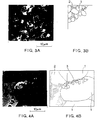
- FIGS. 1A and 1B and FIGS. 2A and 2B Microscope observation results of the structure of a sectional surface of the embodiment target and the reference example target are shown in FIGS. 1A and 1B and FIGS. 2A and 2B.
- the structure of the target according to the reference example exhibited uneven separation of Si 2 and coarse MSi2 1, while the target of the embodiment shown in FIGS. 1A and 1B exhibited a minute and uniform structure wherein MSi2 1 of maximum grain diameter less than 10 ⁇ m was connected in a link form, and Si 2 was distributed in the gaps of the MSi2 1 discontinuously.
- the contents of carbon and oxygen were less than 50 ppm and 100 ppm, respectively, while in the target of the reference example, the contents thereof were approximately 250 ppm and 1,500 ppm, respectively.
- the amount of particles generated from a target according to the embodiments of this invention was much smaller than that according to the reference examples and the conventional examples.
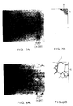
- reference examples and the conventional examples were observed by use of a scanning type electron microscope (SEM), numerous projections 3 were found out on the eroded surfaces of the targets obtained by the reference examples and the conventional examples as shown in FIGS. 4A and 4B.
- SEM scanning type electron microscope
- FIGS. 5A and 5B A result of further magnified observation of a projection 3 having a comparatively large size found on the eroded surfaces of the targets according to the conventional and reference examples is indicated in FIGS. 5A and 5B, and a result of subjecting the surface of the projection 3 shown in FIG. 5A to an element-analysis by use of an X-ray microanalyzer (XMA) is shown in FIG. 6.
- XMA X-ray microanalyzer
- a high purity metal powder made of W, Mo, Ti, Ta, Zr, Hf, Nb, V, Co, Cr or Ni, or a combination thereof and having an average grain diameter of 2 ⁇ m was mixed with a high purity Si powder (containing B, P, Sb, As and other unavoidable elements such as Fe, Ni and else) having an average grain diameter of 20 ⁇ m, at an Si/M atom ratio of 2.6, and the resultant mixed powder was thereafter subjected to a dry mixing process for 72 h in a ball mill, inside of which was replaced by high purity argon gas.
- Thus processed mixed powder was then filled in a hot-press mold made of high purity graphite.
- the entirety was then loaded in a vacuum hot-press and degassed under a vacuum of 6.65 ⁇ 10 ⁇ 3 Pa (5 ⁇ 10 ⁇ 5 Torr) and at a temperature of 1,250°C for 2 h.
- a metal silicide (MSi2) was synthesized at 1,250°C, in a vacuum of 6.65 ⁇ 10 ⁇ 3 Pa (5 ⁇ 10 ⁇ 5 Torr) and under application of 50 kg/cm press-pressure, a metal silicide (MSi2) was synthesized at 1,250°C,. With high purity argon gas added as an internal atmosphere of the hot-press, and with the internal pressure raised to 7.98 ⁇ 104 Pa (600 Torr), the synthesized MSi2 was sintered at 1,370°C for 2 h. The resultant sintered body was then ground and discharge-finished to obtain a target of 260 mm diameter and 6 mm thickness.
- MSi2 metal silicide
- a metal powder of high purity W, Mo, Ti, Ta, Zr, Hf, Nb, Co, Cr or Ni, having a 25 ⁇ m average grain diameter was mixed with a high purity Si powder of 40 ⁇ m average grain diameter at a Si/M atom ratio of 2.6, and then subjected to hot-press under following conditions:
- a WSi2, MoSi2, TaSi2 or TiSi2 powder having an average grain diameter of 80 ⁇ m was mixed with a high purity Si powder having an average grain diameter of 60 ⁇ m, at an Si/M atom ratio of 2.6, and then subjected to hot-press under conditions similar to those of the reference examples 101 to 110, so as to obtain a target having a diameter 260 mm and a thickness 6 mm.
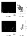
- FIGS. 7A, 7B, 8A, 8B and 9A, 9B respectively.
- a minute mixed structure of the MSi2 phase 1 and Si phase 2 having an average grain diameter of 10 ⁇ m was observed.
- the Si phase 2 and the MSi2 phase 1 were both coarse and large as shown in FIGS. 8A and 8B, and in the case of the target according to the conventional example, it was confirmed that the Si phase 2 and the MSi2 phase 1 were both coarse, as shown in FIGS. 9A and 9B, and formed into a structure easily generating the particles.
- the sputtering surfaces of the targets obtained by the embodiments, reference examples, and conventional examples were observed by a scanning type electron microscope (SEM), and the metal structures as shown in FIGS. 10A, 10B, 11A, 11B, and 12A, 12B were found out. Although a large number of projections 3 were recognized on the sputtering surface of the reference examples (FIGS. 11A, 11B) and the conventional examples (FIGS. 12A, 12B), no projection 3 was observed on the surface of the target according to the embodiments as shown in FIGS. 10A, 10B. It was confirmed from these results that a substantial improvement could be expected in the yield of production by using the target of this invention for forming electrodes and wirings of semiconductor devices.
- SEM scanning type electron microscope
- a sintered silicide substance (tungsten silicide) was cut by wire electrical discharge machining into a diameter of 260 mm, and thereafter the sintered substance was ground to have a thickness of 6 mm by employing a vertical-axis rotary surface grinder with a grinding wheel SD270J55BW6 under conditions: grinding wheel peripheral speed of 1,200 m/min; a table rotating speed of 12 rpm; and a grinding rate of 10 ⁇ m/min.
- the front side surface of the target was worked with a lens polisher and 15 ⁇ m diamond abrasive grains for 60 h, and then with 3 ⁇ m abrasive grains for 10 h.
- An ultrasonic cleaner was used to remove the working solution attached to the lapped surface, and the surface was thereafter degreased by acetone and dried out.
- the roughness of the worked surface was observed with a surface roughness measuring apparatus (Talysurf), and the residual stress in the worked surface was measured with an X-ray stress measuring apparatus on the basis of a parallel-inclination method.
- Table 3 shows the results of these measurements.
- the results of the corresponding measurements of a ground surface, held as it is, are also shown as reference example 200 in the Table 3.
- sputtering was executed by Ar ion irradiation, so that a silicide thin film of 300 nm (3,000 ⁇ ) was deposited on a 12.7 cm (5 inch) Si wafer. The amount of particles contained in the thin film was measured.
- a sintered silicide substance having a diameter of 260 mm was ground and lapped in the same manner as the embodiment 200, and was then polished with an acrylic resin polisher and 0.3 ⁇ m cerium oxide abrasive grains for 10 h under conditions of polisher pressure of 1 kg/cm, and polisher speed of 10 m/min.
- the working solution was removed by ultrasonic cleaning, and the polished surface was thereafter degreased by aceton and was dried, thereby finishing the target.
- Magnetron sputtering was effected by use of this target to form a silicide thin film on a 12.7 cm (five inch) wafer.
- the result of the measurement of the amount of particles mixed in the film is also shown in Table 3. As is apparent from the result, it was confirmed that the amount of particles separated from the target could be remarkably reduced by the improvement in the surface property attained by polishing performed as final finishing.
- a sintered silicide substance having a diameter of 260 mm was ground and lapped in the same manner as the embodiment 200, and was then polished in a mechano-chemical polishing manner by use of a cloth polisher and SiO2 powder of 0.02 ⁇ m for 20 h under a polisher pressure of 1 kg/cm and polisher speed of 10m/min. After ultrasonic cleaning, the polished surface was degreased by aceton and dried, thereby finishing a target.
- a target of high density and having high strength and minute structure, and therefore capable of substantially preventing generation of particles can be provided and therefor it is extremely advantageous for providing a thin film adapted to provide electrodes and wirings of semiconductor devices.
Landscapes
- Chemical & Material Sciences (AREA)
- Engineering & Computer Science (AREA)
- Ceramic Engineering (AREA)
- Manufacturing & Machinery (AREA)
- Materials Engineering (AREA)
- Organic Chemistry (AREA)
- Structural Engineering (AREA)
- Inorganic Chemistry (AREA)
- Chemical Kinetics & Catalysis (AREA)
- Mechanical Engineering (AREA)
- Metallurgy (AREA)
- Physical Vapour Deposition (AREA)
Abstract
Claims (12)
- Cible de pulvérisation cathodique dans laquelle un siliciure de métal (composition stoechiométrique de MSi₂, dans laquelle M est un métal) est couplé sous une forme liée de façon à donner une phase de siliciure de métal, une phase de Si consistant en grains de Si est dispersée de façon discontinue dans les espaces de la phase de siliciure de métal, pour donner à la cible une structure mélangée compacte, et la teneur en carbone dans la structure mélangée est limitée à moins de 100 ppm.
- Cible de pulvérisation cathodique selon la revendication 1, dans laquelle des grains de siliciure de métal en un nombre compris dans une plage allant de 400 à 400 x 10⁴, chaque grain ayant un diamètre de grain dans une plage allant de 5 à 30 µm, sont prévus dans une aire de section de 1 mm de la structure mélangée, et le diamètre de grain maximal des grains de Si est limité à moins de 30 µm.
- Cible de pulvérisation cathodique selon la revendication 1 ou 2, dans laquelle le diamètre moyen des grains de siliciure de métal est dans une plage allant de 2 à 15 µm, tandis que le diamètre moyen des grains de Si est dans une plage allant de 2 à 10 µm.
- Cible de pulvérisation cathodique selon l'une quelconque des revendications 1 à 3, dans laquelle le rapport de densité de la cible est supérieur à 99%.
- Cible de pulvérisation cathodique selon l'une quelconque des revendications 1 à 4, dans laquelle la teneur en oxygène de la cible est limitée à moins de 150 ppm.
- Cible de pulvérisation cathodique selon l'une quelconque des revendications 1 à 5, dans laquelle le métal formant le siliciure de métal est d'au moins une sorte sélectionnée dans le groupe qui comprend le tungstène, le molybdène, le titane, le zirconium, le hafnium, le niobium, le tantale, le vanadium, le cobalt, le chrome et le nickel.
- Cible de pulvérisation cathodique selon l'une quelconque des revendications 1 à 6, dans laquelle une couche d'interface est formée entre la phase de siliciure de métal et la phase de Si.
- Cible de pulvérisation cathodique selon l'une quelconque des revendications 1 à 7, dans laquelle l'épaisseur de la couche d'interface qui est formée entre la phase de siliciure de métal et la phase de Si est fixée dans une plage allant de 10 à 1000 nm (100 à 10000 Å).
- Cible de pulvérisation cathodique selon l'une quelconque des revendications 1 à 8, dans laquelle la phase de Si contient au moins une espèce sélectionnée dans le groupe qui comprend B, P, Sb et As, et des éléments qui sont inévitablement contenus, et la résistivité électrique de la phase de Si est limitée à une plage allant de 0,01 à 100 Ω.cm.
- Procédé de fabrication d'une cible de pulvérisation cathodique dans laquelle un siliciure de métal ayant une composition stoechiométrique exprimée par MSi₂, dans laquelle M représente un métal, est couplée sous une forme liée, de façon à donner une phase de siliciure de métal, et une phase de Si formée par des grains de Si est dispersée de façon discontinue dans les espaces de la phase de siliciure, de manière à donner une structure mélangée compacte pour la cible, et la teneur en carbone dans cette structure mélangée est limitée à moins de 100 ppm, ce procédé comprenant :(I) une étape consistant à mélanger une poudre de métal (M) et une poudre de Si (Si) avec un rapport atomique Si/M allant de 2,0 à 4,0, afin de former une poudre mélangée;(II) une étape consistant à remplir un moule de cette poudre mélangée et à réduire les teneurs en carbone et en oxygène, en chauffant l'ensemble dans un vide poussé, à une température dans la plage allant de 1000 à 1300°C;(III) une étape dans laquelle la poudre mélangée est chauffée dans un vide poussé et sous une pression de compression dans la plage allant de 1 à 10 MPa, pour effectuer la synthèse et le frittage du siliciure de métal; et(IV) une étape dans laquelle le matériau résultant est à nouveau chauffé dans une atmosphère consistant en un vide poussé ou en un gaz inerte, et sous une pression de compression dans la plage allant de 10 à 30 MPa, jusqu'à une température dans la plage de Ts - 50 ≤ T < Ts, en désignant par Ts la température eutectique en °C, de façon à rendre le matériau plus compact.
- Procédé de fabrication d'une cible de pulvérisation cathodique selon la revendication 10, dans lequel la poudre de métal qui est utilisée dans ce procédé est une poudre de métal de haute pureté ayant un diamètre de grain maximal inférieur à 10 pm, tandis que la poudre de Si est une poudre de Si de haute pureté ayant un diamètre de grain maximal inférieur à 30 µm.
- Procédé de fabrication selon la revendication 10 ou 11, dans lequel le processus de réaction, de fusion et de frittage est effectué en utilisant un procédé de compression à chaud ou un procédé de compression isostatique à chaud.
Applications Claiming Priority (3)
| Application Number | Priority Date | Filing Date | Title |
|---|---|---|---|
| JP12305490 | 1990-05-15 | ||
| JP123054/90 | 1990-05-15 | ||
| PCT/JP1991/000639 WO1991018125A1 (fr) | 1990-05-15 | 1991-05-15 | Cible de pulverisation et production de cette derniere |
Publications (3)
| Publication Number | Publication Date |
|---|---|
| EP0483375A1 EP0483375A1 (fr) | 1992-05-06 |
| EP0483375A4 EP0483375A4 (en) | 1992-08-12 |
| EP0483375B1 true EP0483375B1 (fr) | 1996-03-13 |
Family
ID=14851063
Family Applications (1)
| Application Number | Title | Priority Date | Filing Date |
|---|---|---|---|
| EP91909140A Expired - Lifetime EP0483375B1 (fr) | 1990-05-15 | 1991-05-15 | Cible de pulverisation et production de cette derniere |
Country Status (4)
| Country | Link |
|---|---|
| US (3) | US5409517A (fr) |
| EP (1) | EP0483375B1 (fr) |
| DE (1) | DE69117868T2 (fr) |
| WO (1) | WO1991018125A1 (fr) |
Families Citing this family (47)
| Publication number | Priority date | Publication date | Assignee | Title |
|---|---|---|---|---|
| EP0483375B1 (fr) * | 1990-05-15 | 1996-03-13 | Kabushiki Kaisha Toshiba | Cible de pulverisation et production de cette derniere |
| JPH05214523A (ja) * | 1992-02-05 | 1993-08-24 | Toshiba Corp | スパッタリングターゲットおよびその製造方法 |
| US5464520A (en) * | 1993-03-19 | 1995-11-07 | Japan Energy Corporation | Silicide targets for sputtering and method of manufacturing the same |
| JP2794382B2 (ja) * | 1993-05-07 | 1998-09-03 | 株式会社ジャパンエナジー | スパッタリング用シリサイドターゲット及びその製造方法 |
| US6309593B1 (en) * | 1993-07-27 | 2001-10-30 | Kabushiki Kaisha Toshiba | Refractory metal silicide target, method of manufacturing the target, refractory metal silicide thin film, and semiconductor device |
| JP3755559B2 (ja) * | 1997-04-15 | 2006-03-15 | 株式会社日鉱マテリアルズ | スパッタリングターゲット |
| WO1999002288A1 (fr) * | 1997-07-11 | 1999-01-21 | Johnson Matthey Electronics, Inc. | Cibles de pulverisation cathodique d'aluminures et de siliciures intermetalliques, et leurs procedes de fabrication |
| US6569270B2 (en) | 1997-07-11 | 2003-05-27 | Honeywell International Inc. | Process for producing a metal article |
| JP2003535969A (ja) | 1997-07-11 | 2003-12-02 | ジョンソン マッティー エレクトロニクス インコーポレイテッド | 金属間アルミニド及びシリサイドスパッタリングターゲット、及びその製造方法 |
| US6713391B2 (en) | 1997-07-11 | 2004-03-30 | Honeywell International Inc. | Physical vapor deposition targets |
| US6258719B1 (en) | 1998-07-01 | 2001-07-10 | Honeywell International Inc. | Intermetallic aluminides and silicides articles, such as sputtering targets, and methods of making same |
| WO1999003623A1 (fr) * | 1997-07-15 | 1999-01-28 | Tosoh Smd, Inc. | Cibles de pulverisation a base d'un alliage de siliciure et de metal refractaire, utilisation et fabrication correspondante |
| JP2001523767A (ja) | 1997-11-19 | 2001-11-27 | トーソー エスエムディー,インク. | Ni−Siマグネトロンスパッタリングターゲットを製造する方法と該方法によって製造されるターゲット |
| US6348139B1 (en) | 1998-06-17 | 2002-02-19 | Honeywell International Inc. | Tantalum-comprising articles |
| US6183686B1 (en) | 1998-08-04 | 2001-02-06 | Tosoh Smd, Inc. | Sputter target assembly having a metal-matrix-composite backing plate and methods of making same |
| JP3820787B2 (ja) * | 1999-01-08 | 2006-09-13 | 日鉱金属株式会社 | スパッタリングターゲットおよびその製造方法 |
| US6042777A (en) * | 1999-08-03 | 2000-03-28 | Sony Corporation | Manufacturing of high density intermetallic sputter targets |
| US6878250B1 (en) | 1999-12-16 | 2005-04-12 | Honeywell International Inc. | Sputtering targets formed from cast materials |
| US20040072009A1 (en) * | 1999-12-16 | 2004-04-15 | Segal Vladimir M. | Copper sputtering targets and methods of forming copper sputtering targets |
| US6331233B1 (en) | 2000-02-02 | 2001-12-18 | Honeywell International Inc. | Tantalum sputtering target with fine grains and uniform texture and method of manufacture |
| US7517417B2 (en) * | 2000-02-02 | 2009-04-14 | Honeywell International Inc. | Tantalum PVD component producing methods |
| US6803235B1 (en) * | 2000-06-15 | 2004-10-12 | Honeywell International Inc. | Methods of generating information about materials present in compositions and about particulates present in fluids utilizing a microscope |
| US6682636B2 (en) * | 2000-08-18 | 2004-01-27 | Honeywell International Inc. | Physical vapor deposition targets and methods of formation |
| US7153468B2 (en) * | 2000-08-18 | 2006-12-26 | Honeywell International Inc. | Physical vapor deposition targets and methods of formation |
| US6454994B1 (en) * | 2000-08-28 | 2002-09-24 | Honeywell International Inc. | Solids comprising tantalum, strontium and silicon |
| JP4596379B2 (ja) | 2001-07-09 | 2010-12-08 | Jx日鉱日石金属株式会社 | ゲート酸化膜形成用ハフニウムシリサイドターゲット |
| JP3995082B2 (ja) * | 2001-07-18 | 2007-10-24 | 日鉱金属株式会社 | ゲート酸化膜形成用ハフニウムシリサイドターゲット及びその製造方法 |
| US6666901B1 (en) * | 2001-11-08 | 2003-12-23 | Technology Assessment & Transfer, Inc. | Thermal shock resistant quasicrystalline alloy target |
| US7041200B2 (en) * | 2002-04-19 | 2006-05-09 | Applied Materials, Inc. | Reducing particle generation during sputter deposition |
| KR100611904B1 (ko) * | 2002-08-06 | 2006-08-11 | 닛코킨조쿠 가부시키가이샤 | 하프늄 시리사이드 타겟트 및 그 제조방법 |
| WO2004099458A2 (fr) * | 2003-05-02 | 2004-11-18 | Tosoh Smd, Inc. | Procedes de fabrication de cibles de pulverisation en ni-si a faible teneur en silicium et cibles fabriquees par ces procedes |
| JP2005167006A (ja) * | 2003-12-03 | 2005-06-23 | Shin Etsu Chem Co Ltd | フレキシブル金属箔ポリイミド基板の製造方法 |
| JP2007519037A (ja) * | 2003-12-18 | 2007-07-12 | エーエフジー インダストリーズ,インコーポレイテッド | 腐食及び傷耐性を向上させた光学コーティングのため保護層 |
| FR2881757B1 (fr) * | 2005-02-08 | 2007-03-30 | Saint Gobain | Procede d'elaboration par projection thermique d'une cible a base de silicium et de zirconium |
| KR101386806B1 (ko) * | 2005-05-12 | 2014-04-21 | 에이지씨 플랫 글래스 노스 아메리카, 인코퍼레이티드 | 저태양열 획득 계수, 향상된 화학적 및 기계적 특성을 갖는 저방사율 코팅 및 이의 제조 방법 |
| JP4826882B2 (ja) * | 2005-05-18 | 2011-11-30 | 株式会社 アイアイエスマテリアル | スクラップシリコンの選別及び分析方法 |
| US20070099332A1 (en) * | 2005-07-07 | 2007-05-03 | Honeywell International Inc. | Chalcogenide PVD components and methods of formation |
| US20070084527A1 (en) * | 2005-10-19 | 2007-04-19 | Stephane Ferrasse | High-strength mechanical and structural components, and methods of making high-strength components |
| US20070251818A1 (en) * | 2006-05-01 | 2007-11-01 | Wuwen Yi | Copper physical vapor deposition targets and methods of making copper physical vapor deposition targets |
| US20080112878A1 (en) * | 2006-11-09 | 2008-05-15 | Honeywell International Inc. | Alloy casting apparatuses and chalcogenide compound synthesis methods |
| US7901781B2 (en) * | 2007-11-23 | 2011-03-08 | Agc Flat Glass North America, Inc. | Low emissivity coating with low solar heat gain coefficient, enhanced chemical and mechanical properties and method of making the same |
| JP5387613B2 (ja) * | 2010-09-03 | 2014-01-15 | 株式会社豊田中央研究所 | 遷移金属シリサイド−Si複合粉末及びその製造方法、並びに、遷移金属シリサイド−Si複合粉末製造用CaSiy系粉末及びその製造方法 |
| SG11201404314WA (en) * | 2012-02-22 | 2014-10-30 | Jx Nippon Mining & Metals Corp | Magnetic material sputtering target and manufacturing method for same |
| AT15050U1 (de) * | 2015-12-18 | 2016-11-15 | Plansee Composite Mat Gmbh | Beschichtungsquelle mit Strukturierung |
| JP6768575B2 (ja) | 2017-03-24 | 2020-10-14 | Jx金属株式会社 | タングステンシリサイドターゲット及びその製造方法 |
| JP7020123B2 (ja) * | 2018-01-10 | 2022-02-16 | 三菱マテリアル株式会社 | スパッタリングターゲット |
| WO2021193741A1 (fr) * | 2020-03-26 | 2021-09-30 | 東ソー株式会社 | Corps fritté cr-si, cible de pulvérisation, et procédé de production de film fin |
Family Cites Families (23)
| Publication number | Priority date | Publication date | Assignee | Title |
|---|---|---|---|---|
| US2878113A (en) * | 1958-04-17 | 1959-03-17 | Du Pont | Fe-si-ti composition or product and process of preparing same |
| US3285017A (en) * | 1963-05-27 | 1966-11-15 | Monsanto Co | Two-phase thermoelectric body comprising a silicon-germanium matrix |
| US3361560A (en) * | 1966-04-19 | 1968-01-02 | Du Pont | Nickel silicon and refractory metal alloy |
| US3883314A (en) * | 1970-06-29 | 1975-05-13 | Omega Brandt & Freres Sa Louis | Self-lubrication bearing member |
| CA1064736A (fr) * | 1975-06-11 | 1979-10-23 | Robert D. Sturdevant | Compose principal strontique ajoute aux alliages silicium-aluminium en fusion |
| US4135286A (en) * | 1977-12-22 | 1979-01-23 | United Technologies Corporation | Sputtering target fabrication method |
| US4364100A (en) * | 1980-04-24 | 1982-12-14 | International Business Machines Corporation | Multi-layered metallized silicon matrix substrate |
| JPS6066425A (ja) * | 1983-09-22 | 1985-04-16 | Nippon Telegr & Teleph Corp <Ntt> | Lsi電極用の高純度モリブデンタ−ゲツトならびに高純度モリブデンシリサイドタ−ゲツトおよびその製造方法 |
| US4558017A (en) * | 1984-05-14 | 1985-12-10 | Allied Corporation | Light induced production of ultrafine powders comprising metal silicide powder and silicon |
| JPS61179534A (ja) * | 1985-01-16 | 1986-08-12 | Mitsubishi Metal Corp | スパツタリング装置用複合タ−ゲツト |
| US4619697A (en) * | 1984-08-30 | 1986-10-28 | Mitsubishi Kinzoku Kabushiki Kaisha | Sputtering target material and process for producing the same |
| US4750932A (en) * | 1985-04-15 | 1988-06-14 | Gte Products Corporation | Refractory metal silicide sputtering target |
| US4664120A (en) * | 1986-01-22 | 1987-05-12 | Cordis Corporation | Adjustable isodiametric atrial-ventricular pervenous lead |
| JPS63179061A (ja) * | 1987-01-19 | 1988-07-23 | Nippon Mining Co Ltd | 高融点金属シリサイドタ−ゲツトとその製造方法 |
| JPH0791636B2 (ja) * | 1987-03-09 | 1995-10-04 | 日立金属株式会社 | スパツタリングタ−ゲツトおよびその製造方法 |
| JP2594794B2 (ja) * | 1987-08-06 | 1997-03-26 | 株式会社ジャパンエナジー | シリサイドターゲットとその製造方法 |
| US4941920A (en) * | 1987-11-25 | 1990-07-17 | Hitachi Metals, Ltd. | Sintered target member and method of producing same |
| JPH0610345B2 (ja) * | 1987-12-18 | 1994-02-09 | 東京エレクトロン株式会社 | スパッタリング装置 |
| EP0388565B1 (fr) * | 1988-02-11 | 1996-06-05 | STMicroelectronics, Inc. | Chapeau de siliciure de métal réfractaire, pour protéger les structures multicouches de polycide |
| JPH01249619A (ja) * | 1988-03-30 | 1989-10-04 | Toshiba Corp | 高融点金属シリサイドターゲットの製造方法 |
| JP2587872B2 (ja) * | 1988-12-19 | 1997-03-05 | 住友金属鉱山株式会社 | Fe―Si合金軟質磁性焼結体の製造方法 |
| JPH0390319A (ja) * | 1989-09-01 | 1991-04-16 | Sogo Shika Iryo Kenkyusho:Kk | 可視光重合型レジンの連続硬化方法及び装置 |
| EP0483375B1 (fr) * | 1990-05-15 | 1996-03-13 | Kabushiki Kaisha Toshiba | Cible de pulverisation et production de cette derniere |
-
1991
- 1991-05-15 EP EP91909140A patent/EP0483375B1/fr not_active Expired - Lifetime
- 1991-05-15 WO PCT/JP1991/000639 patent/WO1991018125A1/fr not_active Ceased
- 1991-05-15 US US07/793,384 patent/US5409517A/en not_active Expired - Lifetime
- 1991-05-15 DE DE69117868T patent/DE69117868T2/de not_active Expired - Lifetime
-
1994
- 1994-11-21 US US08/345,405 patent/US5508000A/en not_active Expired - Lifetime
-
1995
- 1995-08-09 US US08/512,911 patent/US5612571A/en not_active Expired - Lifetime
Non-Patent Citations (3)
| Title |
|---|
| JOURNAL OF THE JAPAN METAL ASSOCIATION Vol.33 (1994), page 74 * |
| PHILIPS TECHNICAL REVIEW Vol.29, No.2 (1968), pages 45-53 * |
| POWDER METALLURGY, 1964, Vol.7, No.14, pages 168-201 * |
Also Published As
| Publication number | Publication date |
|---|---|
| US5508000A (en) | 1996-04-16 |
| US5409517A (en) | 1995-04-25 |
| DE69117868D1 (de) | 1996-04-18 |
| WO1991018125A1 (fr) | 1991-11-28 |
| EP0483375A1 (fr) | 1992-05-06 |
| US5612571A (en) | 1997-03-18 |
| EP0483375A4 (en) | 1992-08-12 |
| DE69117868T2 (de) | 1996-07-25 |
Similar Documents
| Publication | Publication Date | Title |
|---|---|---|
| EP0483375B1 (fr) | Cible de pulverisation et production de cette derniere | |
| EP0555085B1 (fr) | Procédé pour la fabrication d'une cible de pulvérisation | |
| KR940008020B1 (ko) | 스퍼터링장치용 타겟 | |
| US5733427A (en) | Sputtering target and method of manufacturing the same | |
| JP5562929B2 (ja) | タングステンスパッタリングターゲットおよびその製造方法 | |
| EP0792853B1 (fr) | Procédé de fabrication d'un corps fritté en carbure de silicium | |
| EP0666336B1 (fr) | Procede de production d'une cible en siliciure metallique a point de fusion eleve | |
| JPH05295531A (ja) | Ti−W系スパッタリングターゲットおよびその製造方法 | |
| US6800182B2 (en) | Sputtering target, process for its production and film forming method | |
| JP2757287B2 (ja) | タングステンターゲットの製造方法 | |
| JPH0820863A (ja) | シリサイド膜およびその膜を使用した半導体装置 | |
| JPH10183341A (ja) | タングステンまたはモリブデンターゲット | |
| KR20160067490A (ko) | 텅스텐 폐타겟의 재생방법 및 이로부터 제조된 배선 및 전극 형성을 위한 재활용 텅스텐 타겟 | |
| JP2001295035A (ja) | スパッタリングターゲットおよびその製造方法 | |
| JP5038553B2 (ja) | スパッタリングターゲットの製造方法 | |
| KR20170044343A (ko) | 재활용 텅스텐 타겟의 제조방법 및 이로부터 제조된 재활용 텅스텐 타겟 | |
| KR940010456B1 (ko) | 스퍼터링 타깃 및 그 제조방법 | |
| KR940008016B1 (ko) | 스퍼터링장치용 타겟 및 그 제조방법 | |
| JPH0641629B2 (ja) | スパッタリングターゲットおよびその製造方法 | |
| JP4880809B2 (ja) | スパッタリングターゲットの製造方法およびスパッタリングターゲットならびにそれを用いた金属シリサイド膜、配線、電極、電子部品 | |
| JPWO1991018125A1 (ja) | スパッタリングターゲットおよびその製造方法 |
Legal Events
| Date | Code | Title | Description |
|---|---|---|---|
| PUAI | Public reference made under article 153(3) epc to a published international application that has entered the european phase |
Free format text: ORIGINAL CODE: 0009012 |
|
| 17P | Request for examination filed |
Effective date: 19920110 |
|
| AK | Designated contracting states |
Kind code of ref document: A1 Designated state(s): DE FR GB |
|
| A4 | Supplementary search report drawn up and despatched |
Effective date: 19920622 |
|
| AK | Designated contracting states |
Kind code of ref document: A4 Designated state(s): DE FR GB |
|
| 17Q | First examination report despatched |
Effective date: 19931116 |
|
| GRAA | (expected) grant |
Free format text: ORIGINAL CODE: 0009210 |
|
| AK | Designated contracting states |
Kind code of ref document: B1 Designated state(s): DE FR GB |
|
| REF | Corresponds to: |
Ref document number: 69117868 Country of ref document: DE Date of ref document: 19960418 |
|
| ET | Fr: translation filed | ||
| PLBE | No opposition filed within time limit |
Free format text: ORIGINAL CODE: 0009261 |
|
| STAA | Information on the status of an ep patent application or granted ep patent |
Free format text: STATUS: NO OPPOSITION FILED WITHIN TIME LIMIT |
|
| 26N | No opposition filed | ||
| REG | Reference to a national code |
Ref country code: GB Ref legal event code: 746 Effective date: 19981012 |
|
| REG | Reference to a national code |
Ref country code: FR Ref legal event code: D6 |
|
| REG | Reference to a national code |
Ref country code: GB Ref legal event code: IF02 |
|
| REG | Reference to a national code |
Ref country code: FR Ref legal event code: ST Effective date: 20090119 |
|
| REG | Reference to a national code |
Ref country code: FR Ref legal event code: D3 |
|
| PGFP | Annual fee paid to national office [announced via postgrant information from national office to epo] |
Ref country code: GB Payment date: 20100329 Year of fee payment: 20 |
|
| PGFP | Annual fee paid to national office [announced via postgrant information from national office to epo] |
Ref country code: FR Payment date: 20100525 Year of fee payment: 20 |
|
| PGFP | Annual fee paid to national office [announced via postgrant information from national office to epo] |
Ref country code: DE Payment date: 20100512 Year of fee payment: 20 |
|
| REG | Reference to a national code |
Ref country code: DE Ref legal event code: R071 Ref document number: 69117868 Country of ref document: DE |
|
| REG | Reference to a national code |
Ref country code: GB Ref legal event code: PE20 Expiry date: 20110514 |
|
| PG25 | Lapsed in a contracting state [announced via postgrant information from national office to epo] |
Ref country code: GB Free format text: LAPSE BECAUSE OF EXPIRATION OF PROTECTION Effective date: 20110514 |
|
| PG25 | Lapsed in a contracting state [announced via postgrant information from national office to epo] |
Ref country code: DE Free format text: LAPSE BECAUSE OF EXPIRATION OF PROTECTION Effective date: 20110515 |