EP0483788A2 - Système synchrone de station terminale - Google Patents
Système synchrone de station terminale Download PDFInfo
- Publication number
- EP0483788A2 EP0483788A2 EP91118496A EP91118496A EP0483788A2 EP 0483788 A2 EP0483788 A2 EP 0483788A2 EP 91118496 A EP91118496 A EP 91118496A EP 91118496 A EP91118496 A EP 91118496A EP 0483788 A2 EP0483788 A2 EP 0483788A2
- Authority
- EP
- European Patent Office
- Prior art keywords
- signals
- standby
- working
- transmission
- signal
- Prior art date
- Legal status (The legal status is an assumption and is not a legal conclusion. Google has not performed a legal analysis and makes no representation as to the accuracy of the status listed.)
- Granted
Links
- 230000001360 synchronised effect Effects 0.000 title claims abstract description 59
- 230000005540 biological transmission Effects 0.000 claims abstract description 114
- 238000006243 chemical reaction Methods 0.000 claims description 8
- 238000000034 method Methods 0.000 claims 3
- 238000012986 modification Methods 0.000 claims 2
- 230000004048 modification Effects 0.000 claims 2
- 230000008054 signal transmission Effects 0.000 claims 2
- 230000015654 memory Effects 0.000 description 15
- 238000003780 insertion Methods 0.000 description 5
- 230000037431 insertion Effects 0.000 description 5
- 238000010586 diagram Methods 0.000 description 3
- 230000002159 abnormal effect Effects 0.000 description 2
- 230000004044 response Effects 0.000 description 2
- 230000000694 effects Effects 0.000 description 1
- 230000001105 regulatory effect Effects 0.000 description 1
- 230000000630 rising effect Effects 0.000 description 1
Images


Classifications
-
- H—ELECTRICITY
- H04—ELECTRIC COMMUNICATION TECHNIQUE
- H04L—TRANSMISSION OF DIGITAL INFORMATION, e.g. TELEGRAPHIC COMMUNICATION
- H04L1/00—Arrangements for detecting or preventing errors in the information received
- H04L1/22—Arrangements for detecting or preventing errors in the information received using redundant apparatus to increase reliability
-
- H—ELECTRICITY
- H04—ELECTRIC COMMUNICATION TECHNIQUE
- H04J—MULTIPLEX COMMUNICATION
- H04J3/00—Time-division multiplex systems
- H04J3/02—Details
- H04J3/06—Synchronising arrangements
- H04J3/062—Synchronisation of signals having the same nominal but fluctuating bit rates, e.g. using buffers
- H04J3/0623—Synchronous multiplexing systems, e.g. synchronous digital hierarchy/synchronous optical network (SDH/SONET), synchronisation with a pointer process
-
- H—ELECTRICITY
- H04—ELECTRIC COMMUNICATION TECHNIQUE
- H04J—MULTIPLEX COMMUNICATION
- H04J3/00—Time-division multiplex systems
- H04J3/02—Details
- H04J3/14—Monitoring arrangements
-
- H—ELECTRICITY
- H04—ELECTRIC COMMUNICATION TECHNIQUE
- H04J—MULTIPLEX COMMUNICATION
- H04J2203/00—Aspects of optical multiplex systems other than those covered by H04J14/05 and H04J14/07
- H04J2203/0001—Provisions for broadband connections in integrated services digital network using frames of the Optical Transport Network [OTN] or using synchronous transfer mode [STM], e.g. SONET, SDH
- H04J2203/0046—User Network Interface
- H04J2203/005—Terminal equipment, e.g. codecs, synch
-
- H—ELECTRICITY
- H04—ELECTRIC COMMUNICATION TECHNIQUE
- H04J—MULTIPLEX COMMUNICATION
- H04J2203/00—Aspects of optical multiplex systems other than those covered by H04J14/05 and H04J14/07
- H04J2203/0001—Provisions for broadband connections in integrated services digital network using frames of the Optical Transport Network [OTN] or using synchronous transfer mode [STM], e.g. SONET, SDH
- H04J2203/0057—Operations, administration and maintenance [OAM]
- H04J2203/006—Fault tolerance and recovery
-
- H—ELECTRICITY
- H04—ELECTRIC COMMUNICATION TECHNIQUE
- H04J—MULTIPLEX COMMUNICATION
- H04J2203/00—Aspects of optical multiplex systems other than those covered by H04J14/05 and H04J14/07
- H04J2203/0001—Provisions for broadband connections in integrated services digital network using frames of the Optical Transport Network [OTN] or using synchronous transfer mode [STM], e.g. SONET, SDH
- H04J2203/0089—Multiplexing, e.g. coding, scrambling, SONET
Definitions
- This invention relates to a synchronous terminal station system which synchronously multiplexes a plurality of low order group signals and transmits them to a transmission path.
- a synchronous terminal station system generates a transmission signal which has in each of its frames pointer information that shows the bit time slot in which a leading location of informative data is placed.
- a conventional synchronous terminal station system consists of a large casing frame that is installed on the floor. In side this casing is housed at least one working transmission unit and one standby transmission unit.
- the working transmission unit multiplexes a plurality of frame-synchronized low order group signals, converts them to a high-speed higher order group signal and transmits the signal on a transmission path.
- the synchronous terminal station system also has a monitor circuit to monitor the working transmission unit. When the unit fails the working transmission unit is switched to the standby transmission unit in response to the output of the monitor circuit.
- Such a communication system is disclosed in US Patent 4,601,028.
- the standby transmission unit rather than the working transmission unit will multiplex low order group signals of that group and transmit them.
- each transmission unit is housed independently in separate casing frames, each must have an independent synchronous clock source.
- the clock phase and the frame phase of the low order group signals that are inputted into the standby transmission unit are varied, from one working transmission unit to another from which the low order group signals are inputted. It is also necessary for the standby transmission unit to adjust the clock phase and frame phase of the low order group signals, transferred from any working transmission unit, to a clock phase and frame phase, that are independent of the low order group signals of any working transmission unit.
- each buffer memory must have a memory capacity for one frame of the low order group signal.
- STM-1(STM:Synchronous Transport Module) signals of CCITT Recommendation G.708 are given as the lower order group signals
- high-speed memories of a large capacity equivalent to 19440bits for a frame of a STM-1 signal(155.52Mb/s) are required. This results in the scale of the circuit becoming extremely large.
- the object of this invention is to avoid increasing the scale of the circuitry. This is done by using pointer information, which shows the time slot in a frame where leading portion of the informative transmission data (pay-load frame) is placed.
- a plurality of working synchronous terminal station and one standby synchronous terminal station are housed separately and have different synchronous pulse sources.
- Each working synchronous terminal station receives and multiplexes STM-N signals using its particular synchronous pulse source and outputs the resultant transmission signal on its transmission path.
- the standby synchronous terminal station receives the STM-N signals from a failing working synchronous terminal station and reformats the signals into new frames that are suitable for the standby synchronous terminal station.
- the standby synchronous terminal locates in the signals pointer bytes or information that indicates the position in a frame where the payload frame begins and modifies the value of pointer according to the new frames.
- the reformatted signals with the modified pointer value are then multiplexed within the standby synchronous terminal station and transmitted on a standby transmission path.
- FIG.1 illustrates a block diagram of an embodiment of this invention.
- FIG.2 illustrates a chart which shows a format of a STM-1 signal in the above embodiment.
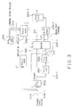
- FIG.3 illustrates a block diagram of an important part of a pointer conversion unit in the above embodiment.
- FIG.4, FIG.5 end FIG.6 illustrates charts to explain the important part of FIG.3.
- FIG.1 illustrates a block diagram of an embodiment of this invention.
- the synchronous terminal station system consists of the working transmission units 100-1 to 100-M for M groups and a standby transmission unit 200. Each unit is housed in individual casing frame.
- the working transmission units 100-1 to 100-M each receive and multiplex N STM-1 signal strings of CCITT recommendation G.708, and transmit them to their respective transmission paths 300-1 to 300-M.
- a different number of STM-1 signals may be inputted into each working transmission unit. This means that all of the working transmission units do not require the same value of N. However, in this case all Ns are the same and hence, the configurations of the working transmission units 100-1 to 100-(M-1) are identical. However, the working transmission unit 100-M has a slightly different configuration from the others. This point will be explained later.
- the working transmission unit 100-1 includes an input section 1, which has interfaces 10-1 to 10-N provided for respective inputs of the STM-1 signals, a pulse generation section 2 for clock pulse and frame pulse signals, a branching section 3 in which one input branches into two outputs, a selection section 4, and a multiplexing and transmission section 5.
- the interfaces 10-1 to 10-N have the same circuit configurations and each of these detects the clock phase and the frame synchronous phase of the input STM-1 signal and adjusts the phases of the input STM-1 signals to be equal to the phase of the clock signal of 155.52Mb/S and the frame synchronous pulse signal from the pulse generation section 2.
- the rate of the frame synchronous pulse is 1/19440 times as fast as the clock signal. Circuits that detect the frame phase of a signal and to synchronize it with a specific frame synchronous pulse are well known.
- FIG.2 illustrates a frame format of a STM-1 signal.
- the signal rate of the STM-1 signal is 155.52Mb/S and the frame length is 19440 bits(2430bytes).
- One frame consists of nine repetitions of a cycle T which consists of nine byte overhead portion and a payload portion (a framed data string having the transmission information from a terminal station).
- the loading nine-byte overhead of a one frame signal string includes a six byte frame synchronous signal (A1, A1, A1, A2, A2, A2), and the other nine byte overhead portion contains the information regulated in CCITT Recommendation G.708.
- the pointers (H1, H2, H3, each three bytes) are placed into the overhead of the fourth cycle T.
- the pointers indicate the number of data bits from the last bit of the pointers to the frame containing the leading position of payload frame.
- the receiving side can then detect the frame leading position in the payload by interpreting the pointers. As shown in FIG.2, where the payload follows immediately after the last bit of the pointers, the values of the pointers indicate the bit number from the leading bit of the payload to the frame containing the leading location of the data strings.
- the leading location of the frame synchronous signals of the inputted STM-1 signals conforms to the frame pulse of the pulse generation section 2 by the effect of interfaces 10-1 to 10-N respectively.
- a clock signal and frame synchronous pulse from the pulse generation section 2, and a STM-1 signal synchronized with them are outputted through separate signal lines from each of the interfaces 10-1 to 10-N.
- the branching section 3 consisting of branching circuits 30-1 to 30-N respectively, splits the clock signals, frame synchronous pulses and synchronized STM-1 signals from interfaces 10-1 to 10-N into two branches.
- the signal lines which link the interfaces, the branching circuits, the selection circuits, the multiplexing section, and pointer interpreting section 221-1 to 222-N are shown as with single lines. However, each of these signal lines actually consists of three lines of the same length as required for the clock signal, the frame synchronous pulse and the STM-1 signal.
- the signals (the clock signals, the frame synchronous pulses and the synchronized STM-1 signals) from the branching circuits 30-1 to 30-N are inputted into the multiplexing circuit 51 and are also inputted into selection circuits 41-1 to 40-N.
- the multiplexing circuit 51 multiplexes the STM-1 signals from the branching circuits 30-1 to 30-N and outputs a multiplexed transmission signal of N-times the signal rate(STM-N). Every STM-1 signal inputted into the multiplexing circuit 51 is adjusted in frame synchronization and clock synchronization, resulting in simple synchronous multiplexing.
- a transmission circuit 52 then transmits the multiplexed signal to the transmission path.
- a monitor 53 monitors the multiplexing section 51, the transmission circuit 52 and the transmission data. When abnormal conditions are detected, the monitor outputs a switching control signal to the selection circuits 40-1 to 40-N, and switches the outputs of the selection circuit to the standby transmission unit 200.
- the selection circuits 40-1 to 40-N in the working transmission unit 100-1 select the clock signal, the frame synchronous pulse and the STM-1 signal from the working transmission unit 100-2 when they don't receive switching control signals from the monitor 53.
- the selection circuit of the working transmission unit 100-M does not output any signals to the working transmission unit 100-(M-1). Under abnormal conditions, it outputs each STM-1 signal to the working transmission unit 100-(M-1).
- the selection circuits of the working transmission units 100-1 to 100-M are necessary for reducing the number of lines between the respective ones and the standby transmission unit. If these circuits are absent, there must be a cable between each of the working transmission units 100-1 to 100-M and a standby transmission unit 200 is required to transmit the split signals from the branching circuits. This results in complex wiring.
- the standby transmission unit 200 includes a pointer conversion section 220, a pulse generator 210 which generates a clock signal at the same rate as the STM-1 signals, and a multiplexing and mission section 230.
- the pointer conversion section 220 includes pointer interpretation sections 221-1 to 221-N, memory circuits 222-1 to 222-N, pointer messing units 223-1 to 223-N and pointer insertion sections 224-1 to 224-N.
- the pointer conversion section receives in parallel the STM-1 signals, the clock signals and the frame synchronous pulse signals from the selection circuits 40-1 to 40-N.
- Each of the selection circuits consists of the same combination of circuits as described above.
- FIG.3 illustrates the pointer insertion section 221-1, the memory circuit 222-1, the pointer processing unit 223-1 and the pointer insertion unit 224-1 in the pointer conversion section 220.
- FIG.4 to FIG.6 are timing charts showing the operations of these components.
- the STM-1 signal, the clock signal and the frame synchronous pulse from the selection circuit 40-1 are converted to a twenty-four bit parallel signal in the S/P (serial/parallel conversion) circuit 250.
- the serial-parallel conversion starts when a frame synchronous pulse is inputted.
- the pointer interpretation circuit 251 detects the location of the pointers H1, H2, H3 based on the parallel signal from the STM-1 signal. In the case of the STM-1 signal, it is easy to detect the pointer location because the number of bits the pointer is located from the frame synchronous pulse A1 - A3 is predetermineded.
- the frame header(FH) generation circuit 252 detects the frames leading to the location of the data strings in the payload which follows H3 in the pointer overhead. This then generates the frame header pulse FH in the corresponding time slot.
- the frame header pulse FH is stored in the memory MEM and is read out by a reading clock pulse which is generated immediately after the storage operation.
- the memory MEM has twenty-four 8 bit parallel-input/parallel-output FIFO memories or registers and can temporally store twenty-four parallel signals ( refer to FIG.4 ) from the S/P circuit 250 in the corresponding MEM.
- This operation is performed by the writing clocks WLPS1 to WLPS8 from the writing clock generator 261 which are shown in FIG.5. While FIG.5 shows only one input of the twenty-four parallel signals, all of the twenty-four parallel signals are written in the twenty-four 8 bit parallel input/output memories by the writing clocks WLPS1 to WLPS8.
- the writing clocks WLPS1 to WLPS8 are not generated during the overhead (OH), but are repeatedly generated during the payload. Therefore, overhead OH is not stored in the memory MEM.
- Every cycle of the writing clocks WLPS1 to WLPS8 consists of 8bits, and generates while shifting by one bit.
- the memory MEM writes new data at every rising edge of WPS1 to WPLS8 ( The length in which the memory can store one bit is longer than the length of the overhead.)
- the readout of the memory MEM is performed at a time when either of the reading clocks RPLS1 to RPLS8 from the reading clock generator 262 are at low levels.
- the reading clocks RPLS1 to RPLS8 generate in synchronization with the clock signal of the pulse generator 210.
- the readout period (low level) extends as long as the length of the overhead.
- the overhead period appears at 90 bit cycle.
- the pointer processing section 223-1 has a counter which is reset to "0" just after detecting the location of the third H3 in the pointer overhead of each frame, as determined from the readout frame (the frame synchronous pulse of the pulse generator 210). (Refer to FIG.6).
- the counter value (778) which shows the frame leading location of the payload, is inserted into the pointer insertion section 224-1 (FIG.6(b), (c)).
- the output of the pointer insertion section 224-1 has no overhead other than the pointers (FIG.6(c)), but the multiplexing circuit 231 inserts or multiplexes the other required overhead at locations which are reserved as shown in the memory output portion of FIG.5.
- the receiving side seperates the multiplexed signals, detects the pointer location from each of the seperated STM-1 signals and calculates the frame leading location of the payload by using the pointer value.
- the standby transmission unit 200 does not shift the phase of the entire frame so as to bring the frame into synchronization with the frame synchronous pulse but instead modifies the pointer value in response to the clock of that unit.
Landscapes
- Engineering & Computer Science (AREA)
- Computer Networks & Wireless Communication (AREA)
- Signal Processing (AREA)
- Computer Hardware Design (AREA)
- Time-Division Multiplex Systems (AREA)
Applications Claiming Priority (2)
| Application Number | Priority Date | Filing Date | Title |
|---|---|---|---|
| JP295036/90 | 1990-10-31 | ||
| JP29503690 | 1990-10-31 |
Publications (3)
| Publication Number | Publication Date |
|---|---|
| EP0483788A2 true EP0483788A2 (fr) | 1992-05-06 |
| EP0483788A3 EP0483788A3 (en) | 1993-03-24 |
| EP0483788B1 EP0483788B1 (fr) | 1998-09-09 |
Family
ID=17815492
Family Applications (1)
| Application Number | Title | Priority Date | Filing Date |
|---|---|---|---|
| EP91118496A Expired - Lifetime EP0483788B1 (fr) | 1990-10-31 | 1991-10-30 | Système synchrone de station terminale |
Country Status (3)
| Country | Link |
|---|---|
| US (1) | US5271001A (fr) |
| EP (1) | EP0483788B1 (fr) |
| DE (1) | DE69130148T2 (fr) |
Cited By (3)
| Publication number | Priority date | Publication date | Assignee | Title |
|---|---|---|---|---|
| WO1995001015A1 (fr) * | 1993-06-23 | 1995-01-05 | Nokia Telecommunications Oy | Procede de transmission de donnees et systeme de transmission de donnees dans un reseau de radiocommunication cellulaire |
| EP0880247A3 (fr) * | 1997-05-20 | 2002-08-21 | Nec Corporation | System de transmission à accès multiples à répartition dans le temps |
| WO2001089121A3 (fr) * | 2000-05-18 | 2003-11-20 | Luminous Networks Inc | Synchronisation de reseaux asynchrones au moyen de symboles de synchronisation en couches par controle d'acces au support |
Families Citing this family (11)
| Publication number | Priority date | Publication date | Assignee | Title |
|---|---|---|---|---|
| JPH04334234A (ja) * | 1991-05-10 | 1992-11-20 | Nec Corp | 多重処理形atmセル誤り訂正回路 |
| JPH0614003A (ja) * | 1991-07-31 | 1994-01-21 | Nec Corp | データ処理回路 |
| JP3203016B2 (ja) * | 1991-09-05 | 2001-08-27 | 富士通株式会社 | 二重化部スタンバイ系からの一重化部に対するアクセス方式 |
| JPH0795225A (ja) * | 1993-09-20 | 1995-04-07 | Fujitsu Ltd | 双方向リングネットワーク制御方式 |
| JP2964207B2 (ja) * | 1993-09-20 | 1999-10-18 | 富士通株式会社 | 現用予備切替制御方式 |
| JPH0964883A (ja) * | 1995-08-24 | 1997-03-07 | Toshiba Corp | 多重化端局装置 |
| DE19607725C1 (de) * | 1996-02-29 | 1997-06-12 | Siemens Ag | Datenübertragungsverfahren |
| JP3407647B2 (ja) * | 1998-03-31 | 2003-05-19 | 安藤電気株式会社 | 多重信号分離回路、伝送誤り測定回路および伝送誤り測定方法 |
| US6195330B1 (en) * | 1998-11-05 | 2001-02-27 | David C. Sawey | Method and system for hit-less switching |
| DE19901588A1 (de) * | 1999-01-16 | 2000-07-20 | Alcatel Sa | Synchronisation eines Netzelementes in einem synchronen digitalen Nachrichtenübertragungsnetz |
| US6515962B1 (en) | 1999-07-16 | 2003-02-04 | Alcatel | Hit-less switching pointer aligner apparatus and method |
Family Cites Families (7)
| Publication number | Priority date | Publication date | Assignee | Title |
|---|---|---|---|---|
| US4497054A (en) * | 1983-04-29 | 1985-01-29 | Honeywell Inc. | One-for-N redundancy in a digital switch matrix |
| JPS60254928A (ja) * | 1984-05-31 | 1985-12-16 | Nec Corp | セツト・スタンバイ通信方式 |
| US4601028A (en) * | 1984-06-18 | 1986-07-15 | Rockwell International Corporation | Method of and apparatus for checking datapath failure in a communication muldem |
| JPS62253231A (ja) * | 1986-01-07 | 1987-11-05 | Fujitsu Ltd | 現用予備切換システム |
| US4964112A (en) * | 1988-06-01 | 1990-10-16 | Siemens Aktiengesellschaft | Method for monitoring the quality of a digital signal in sections of a data transmission circuit |
| EP0360924B1 (fr) * | 1988-09-22 | 1993-12-29 | Siemens Aktiengesellschaft | Procédé de contrôle de centraux de télécommunications à division dans le temps commandés par horloge, en particulier des centraux téléphoniques MIC avec des réseaux de commutation distribués, connectés à un réseau de commutation central |
| US5051979A (en) * | 1990-06-28 | 1991-09-24 | At&T Bell Laboratories | Method and apparatus for errorless switching |
-
1991
- 1991-10-30 US US07/784,599 patent/US5271001A/en not_active Expired - Fee Related
- 1991-10-30 DE DE69130148T patent/DE69130148T2/de not_active Expired - Fee Related
- 1991-10-30 EP EP91118496A patent/EP0483788B1/fr not_active Expired - Lifetime
Cited By (5)
| Publication number | Priority date | Publication date | Assignee | Title |
|---|---|---|---|---|
| WO1995001015A1 (fr) * | 1993-06-23 | 1995-01-05 | Nokia Telecommunications Oy | Procede de transmission de donnees et systeme de transmission de donnees dans un reseau de radiocommunication cellulaire |
| AU681890B2 (en) * | 1993-06-23 | 1997-09-11 | Nokia Telecommunications Oy | Data transmission method and data transmission system in a cellular radio network |
| US5715245A (en) * | 1993-06-23 | 1998-02-03 | Nokia Telecommunications Oy | Data transmission from a controller to successive bases stations linked in series |
| EP0880247A3 (fr) * | 1997-05-20 | 2002-08-21 | Nec Corporation | System de transmission à accès multiples à répartition dans le temps |
| WO2001089121A3 (fr) * | 2000-05-18 | 2003-11-20 | Luminous Networks Inc | Synchronisation de reseaux asynchrones au moyen de symboles de synchronisation en couches par controle d'acces au support |
Also Published As
| Publication number | Publication date |
|---|---|
| US5271001A (en) | 1993-12-14 |
| DE69130148T2 (de) | 1999-01-28 |
| DE69130148D1 (de) | 1998-10-15 |
| EP0483788A3 (en) | 1993-03-24 |
| EP0483788B1 (fr) | 1998-09-09 |
Similar Documents
| Publication | Publication Date | Title |
|---|---|---|
| EP0483788B1 (fr) | Système synchrone de station terminale | |
| US4716561A (en) | Digital transmission including add/drop module | |
| JP2591295B2 (ja) | フレーム位相同期方式 | |
| JPH05183530A (ja) | 同期ペイロードポインタ処理方式 | |
| JP3290534B2 (ja) | パスプロテクションスイッチ装置 | |
| US6188685B1 (en) | Synchronous digital transmission system | |
| US5892770A (en) | Process for converting digital data streams having an ATM cell structure | |
| US5325354A (en) | Synchronous terminal station receiving system | |
| EP0543327B1 (fr) | Système synchrone de multiplexage optique | |
| US5267236A (en) | Asynchronous parallel data formatter | |
| US4905228A (en) | Digital transmission channel framing | |
| US4924459A (en) | Digital transmission interconnect signal | |
| US7016344B1 (en) | Time slot interchanging of time slots from multiple SONET signals without first passing the signals through pointer processors to synchronize them to a common clock | |
| US20020026568A1 (en) | Serial data mapping apparatus for synchronous digital hierarchy | |
| EP0944279B1 (fr) | Circuit d'affectation d'intervalles temporels | |
| JPH09321723A (ja) | 無瞬断回線切替え装置及び方法 | |
| JP2715753B2 (ja) | 同期端局装置 | |
| CN1155177C (zh) | 数据流的适配与连接的方法和电路装置 | |
| JPH08223130A (ja) | 無瞬断切替方式 | |
| EP0220808A2 (fr) | Multiplexeur pour signaux numériques | |
| JPH07141250A (ja) | メモリ制御装置 | |
| JP2868026B2 (ja) | 非同期転送モード用の多重化装置およびその試験装置 | |
| JPH0834461B2 (ja) | フレ−ムアライナ回路 | |
| JP2976732B2 (ja) | 同期光多重化装置 | |
| US20090161698A1 (en) | Method and apparatus for data processing |
Legal Events
| Date | Code | Title | Description |
|---|---|---|---|
| PUAI | Public reference made under article 153(3) epc to a published international application that has entered the european phase |
Free format text: ORIGINAL CODE: 0009012 |
|
| 17P | Request for examination filed |
Effective date: 19911128 |
|
| AK | Designated contracting states |
Kind code of ref document: A2 Designated state(s): DE FR GB |
|
| PUAL | Search report despatched |
Free format text: ORIGINAL CODE: 0009013 |
|
| AK | Designated contracting states |
Kind code of ref document: A3 Designated state(s): DE FR GB |
|
| 17Q | First examination report despatched |
Effective date: 19950627 |
|
| GRAG | Despatch of communication of intention to grant |
Free format text: ORIGINAL CODE: EPIDOS AGRA |
|
| GRAG | Despatch of communication of intention to grant |
Free format text: ORIGINAL CODE: EPIDOS AGRA |
|
| GRAG | Despatch of communication of intention to grant |
Free format text: ORIGINAL CODE: EPIDOS AGRA |
|
| GRAH | Despatch of communication of intention to grant a patent |
Free format text: ORIGINAL CODE: EPIDOS IGRA |
|
| GRAH | Despatch of communication of intention to grant a patent |
Free format text: ORIGINAL CODE: EPIDOS IGRA |
|
| GRAA | (expected) grant |
Free format text: ORIGINAL CODE: 0009210 |
|
| AK | Designated contracting states |
Kind code of ref document: B1 Designated state(s): DE FR GB |
|
| REF | Corresponds to: |
Ref document number: 69130148 Country of ref document: DE Date of ref document: 19981015 |
|
| ET | Fr: translation filed | ||
| PLBE | No opposition filed within time limit |
Free format text: ORIGINAL CODE: 0009261 |
|
| STAA | Information on the status of an ep patent application or granted ep patent |
Free format text: STATUS: NO OPPOSITION FILED WITHIN TIME LIMIT |
|
| 26N | No opposition filed | ||
| PGFP | Annual fee paid to national office [announced via postgrant information from national office to epo] |
Ref country code: FR Payment date: 20011010 Year of fee payment: 11 |
|
| PGFP | Annual fee paid to national office [announced via postgrant information from national office to epo] |
Ref country code: GB Payment date: 20011031 Year of fee payment: 11 |
|
| PGFP | Annual fee paid to national office [announced via postgrant information from national office to epo] |
Ref country code: DE Payment date: 20011112 Year of fee payment: 11 |
|
| REG | Reference to a national code |
Ref country code: GB Ref legal event code: IF02 |
|
| PG25 | Lapsed in a contracting state [announced via postgrant information from national office to epo] |
Ref country code: GB Free format text: LAPSE BECAUSE OF NON-PAYMENT OF DUE FEES Effective date: 20021030 |
|
| PG25 | Lapsed in a contracting state [announced via postgrant information from national office to epo] |
Ref country code: DE Free format text: LAPSE BECAUSE OF NON-PAYMENT OF DUE FEES Effective date: 20030501 |
|
| GBPC | Gb: european patent ceased through non-payment of renewal fee | ||
| PG25 | Lapsed in a contracting state [announced via postgrant information from national office to epo] |
Ref country code: FR Free format text: LAPSE BECAUSE OF NON-PAYMENT OF DUE FEES Effective date: 20030630 |
|
| REG | Reference to a national code |
Ref country code: FR Ref legal event code: ST |