EP0484545A1 - Elektroden- und elektrodenleitungsstruktur eines piezoelektrischen resonators aus einer ultradünnen schicht - Google Patents
Elektroden- und elektrodenleitungsstruktur eines piezoelektrischen resonators aus einer ultradünnen schicht Download PDFInfo
- Publication number
- EP0484545A1 EP0484545A1 EP91908864A EP91908864A EP0484545A1 EP 0484545 A1 EP0484545 A1 EP 0484545A1 EP 91908864 A EP91908864 A EP 91908864A EP 91908864 A EP91908864 A EP 91908864A EP 0484545 A1 EP0484545 A1 EP 0484545A1
- Authority
- EP
- European Patent Office
- Prior art keywords
- electrode
- ultrathin
- resonator
- piezoelectric
- piezoelectric plate
- Prior art date
- Legal status (The legal status is an assumption and is not a legal conclusion. Google has not performed a legal analysis and makes no representation as to the accuracy of the status listed.)
- Granted
Links
Images


Classifications
-
- H—ELECTRICITY
- H10—SEMICONDUCTOR DEVICES; ELECTRIC SOLID-STATE DEVICES NOT OTHERWISE PROVIDED FOR
- H10N—ELECTRIC SOLID-STATE DEVICES NOT OTHERWISE PROVIDED FOR
- H10N30/00—Piezoelectric or electrostrictive devices
- H10N30/80—Constructional details
- H10N30/87—Electrodes or interconnections, e.g. leads or terminals
-
- H—ELECTRICITY
- H03—ELECTRONIC CIRCUITRY
- H03H—IMPEDANCE NETWORKS, e.g. RESONANT CIRCUITS; RESONATORS
- H03H9/00—Networks comprising electromechanical or electro-acoustic elements; Electromechanical resonators
- H03H9/02—Details
- H03H9/125—Driving means, e.g. electrodes, coils
- H03H9/13—Driving means, e.g. electrodes, coils for networks consisting of piezoelectric or electrostrictive materials
- H03H9/132—Driving means, e.g. electrodes, coils for networks consisting of piezoelectric or electrostrictive materials characterized by a particular shape
-
- H—ELECTRICITY
- H03—ELECTRONIC CIRCUITRY
- H03H—IMPEDANCE NETWORKS, e.g. RESONANT CIRCUITS; RESONATORS
- H03H9/00—Networks comprising electromechanical or electro-acoustic elements; Electromechanical resonators
- H03H9/02—Details
- H03H9/05—Holders or supports
- H03H9/10—Mounting in enclosures
- H03H9/1007—Mounting in enclosures for bulk acoustic wave [BAW] devices
- H03H9/1014—Mounting in enclosures for bulk acoustic wave [BAW] devices the enclosure being defined by a frame built on a substrate and a cap, the frame having no mechanical contact with the BAW device
-
- H—ELECTRICITY
- H03—ELECTRONIC CIRCUITRY
- H03H—IMPEDANCE NETWORKS, e.g. RESONANT CIRCUITS; RESONATORS
- H03H9/00—Networks comprising electromechanical or electro-acoustic elements; Electromechanical resonators
- H03H9/15—Constructional features of resonators consisting of piezoelectric or electrostrictive material
- H03H9/17—Constructional features of resonators consisting of piezoelectric or electrostrictive material having a single resonator
- H03H9/177—Constructional features of resonators consisting of piezoelectric or electrostrictive material having a single resonator of the energy-trap type
-
- H—ELECTRICITY
- H03—ELECTRONIC CIRCUITRY
- H03H—IMPEDANCE NETWORKS, e.g. RESONANT CIRCUITS; RESONATORS
- H03H9/00—Networks comprising electromechanical or electro-acoustic elements; Electromechanical resonators
- H03H9/46—Filters
- H03H9/54—Filters comprising resonators of piezoelectric or electrostrictive material
- H03H9/56—Monolithic crystal filters
Definitions
- the present invention relates to electrodes and their lead structure of an ultrathin piezoelectric resonator whose fundamental frequency is as high as tens to hundreds of megahertz.
- An ordinary AT cut quartz crystal resonator which has heretofore been used widely as a piezoelectric device (such as a resonator or filter), has a very excellent temperature-frequency characteristic; however, since its resonance frequency is in inverse proportion to the thickness of AT cut quartz crystal plate , the fundamental frequency of this kind of resonator with a mechanical strength sufficient for practical use is around 40 MHz at the highest.
- overtone oscillation means which extracts a higher order harmonic mode vibration of an AT cut quartz crystal resonator to obtain a frequency which is an odd multiple of the fundamental resonance frequency, but its oscillation circuit calls for an LC tuning circuit including a coil, and hence is not suitable for fabrication as a semiconductor IC, besides the overtone oscillation circuit may sometimes be difficult to activate because such a resonator has a large capacitance ratio and consequently a high impedance level.
- a surface acoustic wave resonator whose oscillation frequency is determined by the pitch of electrode fingers of an interdigital transducer, has come to be able to output a maximum of 1 GHz or so due to the progress in photolithography, the resonator of this kind possesses a problem as a piezoelectric substrate usable therefor is remarkably inferior to the AT cut quartz crystal in terms of temperature-frequency characteristic.
- the piezoelectric resonator has a cavity 2 provided by machining or etching in one side of a block of AT cut quartz crystal 1 centrally thereof to form a vibratory portion 3, which has a thickness of about 17 ⁇ m, if a fundamental resonance frequency of, say, 100 MHz is desired to obtain.
- the ultrathin vibratory portion 3 is edged with and mechanically supported by a thick frame-like marginal portion (or rib) 4 formed integrally therewith.
- a conductive film 5 all over the piezoelectric substrate on the side where the cavity 2 is provided and by depositing a partial electrode 6 and an electrode lead 7 extending therefrom, through use of, for example, vacuum evaporation on the flat surface of the vibratory portion 3 opposite from the cavity 2, it is possible to obtain a resonator of a very high resonance frequency substantially equal to the fundamantal resonant frequency of the ultrathin vibratory portion 3 or a filter element of such a high center frequency.
- the above-said piezoelectric resonator is suitable for housing in such a flat package as depicted in Fig. 17.
- the conductive film 10 on the bottom of the concavity of the case 8 is connected to a terminal 11 formed at one corner of the case 8 on the underside thereof via a connecting conductor hermetically passing through the case 8.
- a pad 7a at one end of the electrode lead 7 extending from the partial electrode 6 of the resonator has a minimum area necessary for connection, by a bonding wire 12, to a pad 14 formed on a stepped portion 13 on the inside of the case 8.
- the pad 14 is also connected to a terminal 15 provided at another corner of the case 8 on the underside thereof via a connecting conductor which hermetically passes through the case 8.
- the above-described ultrathin resonator studied so for has the overall electrode 5 on the side of the piezoelectric block (i.e.the piezoelectric plate) 1 where the cavity 2 is provided, and hence is easy to manufacture, but the overall electrode 5 and the electrode lead portion 7 extending from the partial electrode 6 are deposited on both sides of the ultrathin vibratory portion 3 and they constitute a capacitor of a large capacity, which causes an increase in a parallel capacitance C0 in an equivalent circuit of the piezoelectric resonator shown in Fig. 18.
- VXO voltage controlled quartz crystal oscillator
- the present invention is intended to solve the above-mentioned problems of the ultrathin piezoelectric resonator which have been left unsolved so far, and it is a first object of the invention to provide an electrode structure of an ultrathin piezoelectric resonator which is free from various drawbacks attributable to an increase in an equivalent parallel capacitance of the resonator which results from the formation of a capacitor between the overall electrode and the electrode lead portion deposited on both sides of the ultrathin vibratory portion forming the bottom of the cavity made in one side of a block of a piezoelectric material such as quartz crystal.
- the width (the sectional area) of the electrode lead portion 7 extending from the partial electrode 6 deposited opposite the overall electrode 5 on the bottom of the cavity of the piezoelectric plate 1 is selected large enough to make the ohmic loss(i.e. the electrode resistance) negligible, then a resonance is caused by the electrode lead portion 7 serving as a dummy electrode in the vicinity of the point of resonance by the afore mentioned true electrode and the resonance becomes a high-level spurious .
- aluminum is suitable for use as an electrode material, taking into account the thicknesses of the electrodes 5 and 6 large enough to secure their conductivity and the mass loading effect for entrapping the vibration energy on the partial electrode 6.
- the electrodes are thinner than 500 ⁇ , current does not readily flow therethrough, no matter what metal may be used, and hence the electrodes must be formed more than 500 ⁇ thick, but if they are formed thick using a metal of a large density, such as gold, the resonance frequency is excessively reduced by the electrodes; therefore, it is preferable to use aluminum which is a light weight electrode material.
- the surface of the aluminum readily oxizies to form alumite which is a highly insulating material.
- the conductive film 10 on the bottom of the package and the overall electrode 5 are electrically connected by the conductive adhesive 9, conductivity therebetween is insufficient, and consequently, they constitute a capacitance; in the case of an oscillator, an increase in its capacitance ratio will limit the variable range of the oscillation frequency, and in the case of a multimode filter element, the overall electrode 5 will serve as an earth electrode and no sufficient grounding is effected, resulting in the attenuation of the filter becoming insufficient.
- a third object of the present invention is to provide an electrode lead structure of the ultrathin piezoelectric resonator which is overcomes the problem of bad conductivity between the electrode lead portion of the resonator and the conductive film of the package leading to its external lead which is caused by the formation of oxide films on the surfaces of the electrode lead portion and the conductive film, so as to improve characteristics of the piezoelectric resonator.
- the electrode lead portion which extends from the partial electrode provided on one surface of the ultrathin vibratory portion toward one marginal edge of the piezoelectric plate, is formed sufficiently narrow on the vibratory portion but sufficiently wide on the frame-like marginal portion.
- an unetched portion is utilized to increase the wide area of the electrode lead portion and reduce its narrow portion to thereby further reduce the ohmic loss.
- the conductive film forming the overall electrode is removed from at least the area corresponding to the electrode lead portion on the ultrathin vibratory portion on the opposite side therefrom.
- portion of electrode lead patterns extending from the partial electrode which is deposited on the ultrathin vibratory portion is formed by a plurality of narrow electrode lead patterns.
- the electrode lead portion extending from the partial electrode toward the frame-like marginal portion and the overall electrode deposited opposite thereto are electrically connected through a through hole made in the frame-like marginal portion thickwise thereof at an appropriate position or a recess made in one end face of the frame-like marginal portion and a pad on the resonator and a pad leading to an external lead of the package are connected by a wire bonding.
- Fig. 1 is a plane view illustrating an example of the electrode lead structure of the ultrathin piezoelectric resonator according to a first embodiment of the present invention
- Figs. 2(a) and (b) are a sectional view and a plane view illustrating an example of the electrode lead structure of the ultrathin piezoelectric resonator according to a second embodiment of the present invention
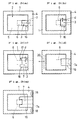
- Figs. 3(a) through (e) are plane views showing different examples of the electrode structure of the ultrathin piezoelectric resonator according to a third embodiment of the present invention
- Fig. 4 is a plane view illustrating the basic structure of a fourth embodiment of the present invention
- Fig. 1 is a plane view illustrating an example of the electrode lead structure of the ultrathin piezoelectric resonator according to a first embodiment of the present invention
- Figs. 2(a) and (b) are a sectional view and a plane view illustrating an example of the electrode lead structure of the ultrathin piez
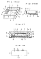
- FIG. 5 is a plane view showing the application of the fourth embodiment to such an ultrathin block of the piezoelectric material as shown in Fig. 6(a) through (c) are a plane view illustrating an example of a piezoelectric resonator employing an ultrathin piezoelectric plate in accordance with a fifth embodiment of the present invention and sectional views respectively taken on the lines A-A and B-B in Fig. 6(a);
- Fig. 7 is a plane view illustrating an example of an ultrathin multimode filter element employing the first embodiment of the present invention;
- Fig. 8 is a plane view showing an example of an ultrathin multimode filter element utilizing the second embodiment of the present invention;
- FIG. 9(a) and (b) are plan views showing different examples of ultrathin multimode filter elements employing the third embodiment of the present invention
- Fig. 10 is a plane view illustrating an embodiment of an ultrathin multimode filter element employing the fourth embodiment of the present invention
- Fig. 11 is a plan view showing a multimode filter element employing the fifth embodiment of the present invention
- Fig. 12 is a graph showing a characteristic of the filter element depicted in Fig. 11
- Fig. 13 is a plan view illustrating an embodiment of a multimode filter element provided with a shield electrode
- Figs. 14(a) and (b) are a plane view showing the construction of a through hole and a sectional view taken on the line C-C in Fig. 14(a); Figs.
- FIGS. 15(a) and (b) are a perspective view of a modified from of the multimode filter element employing the fifth embodiment of the present invention and a diagram showing a manufacturing process of the piezoelectric plate;
- Figs. 16(a) and (b) are a perspective view illustrating the construction of a conventional ultrathin piezoelectric resonator and a sectional view taken on the line X-X in Fig. 16(a);
- Fig. 17 is a sectional view showing its packaging method;
- Fig. 18 is an equivalent circuit of a resonator;
- FIg. 19 is a plane view showing an ultrathin piezoelectric resonator having an electrode lead of about the same width as that of the partial electrode.
- the ultrathin piezoelectric resonator employs the electrode structure which has the overall electrode deposited on the piezoelectric substrate on the side where the cavity is provided and the partial electrode on the opposite side therefrom.
- the partial electrode is formed on the vibratory portion in the cavity of the piezoelectric substrate and the narrow electrode lead which extends from the partial electrode climbing over the inner wall of the cavity and a stepped portion contiguous thereto, although the formation of the partial electrode and its lead portion can be carried out by a troublesome method which involves tilting the piezoelectric substrate during the vapor deposition, and in this instance it is not sure to secure the conduction of the electrode lead portion.
- the overall electrode is formed on the side where the cavity is provided.
- the resonator of this type is intended primarily for microminiaturization and it is desirable that the piezoelectric substrate has a size of 3 mm by 3mm or less, for example.
- the present invention utilizes a method by which a number of chips are formed on one piezoelectric wafer by batch processing and the wafer is cut into individual chips.
- the overall electrode can be formed simply by evaporating a conductive film all over one side of the wafer and no photomask or mask for photolithography is needed-this improves the efficiency of production, i.e. the yield rate of product, and hence affords reduction of manufacturing costs.
- the ultrathin piezoelectric resonator studied by the inventors so far has the overall electrode deposited on the substrate on the side where the cavity is formed.
- the vibratory portion is so thin that a large capacitance is formed between the overall electrode and the extending from the partial electrode lead portion deposited on both sides of the vibratory portion, and as a result, the capacitance ratio of the resonator becomes large, introducing various disadvantages.
- the ultrathin piezoelectric resonator of the present invention employs such an electrode structure as mentioned below.
- Fig. 1 is a plane view illustrating the basic construction of a first embodiment of the present invention which is intended to attain the afore-mentioned first object of the invention.
- the width of that portion 7a of the electrode lead 7 extending from the partial electrode 6 which corresponds to the width of the frame-like marginal portion 4 is sufficiently larger than the other portion 7b of the electrode lead , the partial electrode 6 being deposited on the side opposite from the overall electrode 5 formed on the ultrathin piezoelectric block 1 on the side where the cavity 2 is provided.
- the reason for which the width of the electrode lead portion 7b lying on the vibratory portion 3 is minimized but the width of the electrode lead portion 7a lying on the frame-like marginal portion 4 is made large is as follows;
- the vibratory portion 3 is so thin that if wide conductive films are present on both sides thereof in opposing relation to each other, they form a large capacitance, whereas the frame-like marginal portion 4 is so thick that if conductive films are present on both sides thereof, they do not constitute a large capacitance, and hence the capacitance ratio ⁇ of the resonator is not seriously affected.
- the ohmic loss can be reduced by minimizing the length of the narrow electrode lead portion 7b.
- the capacitance ratio of the ultrathin piezoelectric resonator it is possible to suppress the capacitance ratio of the ultrathin piezoelectric resonator to a low value and secure a sufficiently wide variable range of its resonance frequency.
- the area of the electrode lead portion on the vibratory portion of the resonator is smaller than the area of the partial electrode, the generation of unwanted vibration is also negligible.
- Such an electrode structure as shown in Fig. 2 is effective in further reductions of the capacitance ratio ⁇ of the resonator and the ohmic loss.
- Figs. 2(a) and (b) are a sectional view and a plane view illustrating a second embodiment of the present invention intended to attain the first object of the invention.
- unetched portions 20 and 22 are formed on the inner wall of the cavity 2 at a substantially constant angle of inclination in +x and -x directions, respectively, as shown in Fig. 2 (a) . Consequently, the inner wall of the cavity 2 formed by etching does not form a vertical wall from the frame-like marginal portion 4 to the vibratory portion 3, but instead the unetched inclined portion of widths l1 and l2 are formed between the vibratory portion 3 and the frame-like marginal portion 4.
- the slope of the unetched portion 20 in the +x direction is gentler than the slope of the unetched portion 22 in the -x direction, that is, l1 > l2.
- the electrode lead pattern 7 extending between the conductor pad 7a and the partial electrode 6 is narrow but is shortened by l1. This affords further reduction of the ohmic loss of the electrode lead portion 7 and permits holding low the capacitance between the electrode lead portion 7 and the overall electrode 5.
- Figs. 3(a) through (e) illustrate a third embodiment of the present invention intended to attain its first object.
- Fig. 3(a) is a plane view showing its basic construction, wherein that portion 16 of the overall electrode 5 deposited on the bottom of the cavity 2 of the ultrathin piezoelectric block 1 which corresponds to the electrode lead portion 7 extending on the vibratory portion 3 from the partial electrode 6 is removed.
- the distance d between the marginal edge of the electrode lead portion 7 and the corresponding marginal edge of that portion 16 of the overall electrode 5 which is to be removed is selected nearly equal to the thickness of the frame-like marginal portion 4 as shown in Fig. 3(b) so thatthe capacitance formed by the electrodes on both sides of the vibratory portion 3 can be made substantially negligible.
- a capacitance is formed between the lead portion 7 of the partial electrode 6 and the conductive film extending to the position corresponding to the marginal edge of the partial electrode 6 contiguous to the lead portion 7.
- the formation of such a capacitance can effectively be prevented by removing not only the above-mentioned portion 16 but also that portion 17 of the overall electrode 5 which corresponds to the above-noted marginal edge of the partial electrode 6, as shown in Fig. 3(c).
- the overall electrode is not always deposited over the entire area of that side of the piezoelectric block 1 where the cavity 2 is formed, it is self-evident that such an electrode structure increases the number of manufacturing steps and inevitably raises the manufacturing costs; however, the electrode structure makes it possible to meet a customer's specific requirement, for example, a demand for a resonator for a voltage controlled quartz crystal oscillator of a very wide variable frequency range--this more than offsets increased manufacturing costs.
- the width of the electrode lead portion 7 on the ultrathin vibratory portion 3 becomes about the same as the width of the partial electrode 6 as shown in Fig. 19, because the partial electrode 6 itself is very small.
- the overall electrode 5 and the electrode lead portion 7b deposited on both sides of vibratory portion 3 act as dummy electrodes and a spurious resonance of large level is caused by the electrode lead portion 7b in the vicinity of the point of resonance by the true electrode 6 as referred to previously.
- the ultrathin piezoelectric resonator according to the fourth embodiment of the present invention uses such an electrode structure as described below.
- Fig. 4 is a plane view showing the basic structure of the fourth embodiment of the present invention, wherein that portion of the electrode lead 7 extending from the partial electrode 6 deposited opposite the overall electrode 5 on the piezoelectric block 1 which lies on the ultrathin vibratory portion 3 is formed by a plurality of narrow electrode lead patterns 7c, 7c, ... in such a manner that the sum of their sectional areas may be sufficiently large enough to prevent an increase in the ohmic loss.
- the three electrode lead patterns 7c are extended from the partial electrode 6 to the pad 7a on the marginal portion of the piezoelectric block 1 but this is intended as being merely illustrative and the number of electrode lead patterns 7c may be two or more. Moreover, the electrode lead patterns need not always be parallel to each other.
- the area of the pad 7a can be set arbitrarily, because it lies on the thick frame-like marginal portion 4 and has nothing to do with the resonance of the vibratory portion 3 (even if it resonates, its resonance frequency is very lower than that of the resonance of the vibratory portion).
- the electrode structure of this embodiment is markedly effective in maintaining the spurious resonance characteristic of the easy-to-manufacture ultrathin piezoelectric resonator with the overall electrode deposited over one side of the piezoelectric block 1 without increasing its equivalent resistance.
- Fig. 5 shows an application of the electrode structure of the fourth embodiment to the ultrathin piezoelectric block 1 including such unetched portions 20 and 22 as depicted in Fig. 2.
- the pad 7a lying on the frame-like marginal portion 4 is extended to the portion corresponding to the unetched portion 20 and the electrode lead portion 7 on the vibratory portion 3 is formed by a plurality of narrow electrode lead patterns 7b.
- the area of the electrode lead pattern 7b is shortend--this affords further reduction of the level of the spurious by the electrode lead portion 7b and, at the same time, decreases the ohmic loss of the electrode lead portion and the equivalent parallel capacitance of the resonator.
- the ultrathin piezoelectric resonator is suitable for housing in, for example, a ceramic-sintered dish-like package such as shown in Fig. 17. That is, it is effective in simplifying the manufacturing process of the device to house the piezoelectric block 1 with the cavity 2 facing down toward the bottom of the package 8 and electrically connect and mechanically fix the aluminum electrode film 5 on the frame-like marginal portion 4 of the block 1 and the aluminum film 10 on the bottom of the package 8 through use of the conductive adhesive 9.
- the third object of the present invention is to solve the above-mentioned problem of the ultrathin piezoelectric resonator.
- Fig. 6(a), (b) and (c) are a plane view showing the state in which the resonator using the ultrathin piezoelectric plate according to the present invention is fixedly mounted in the package, a sectional view taken on the line A-A in Fig. 6(a) and a sectional view taken on the line B-B in Fig. 6(a) , respectively.
- the ultrathin piezoelectric plate has the cavity 2 formed by mechanical grinding or etching in one side of, for example, a rectangular parallelepipedic AT cut quartz crystal block 1 substantially centrally thereof to form the ultrathin vibratory portion 3 mechanically supported by the surrounding thick frame-like marginal portion 4 formed integrally therewith.
- the quartz crystal block 1 of such a configuration has the overall electrode 5 formed by a conductive film deposited all over the block 1 on the side where the cavity 2 is provided and has, on the flat side of the vibratory portion 3 opposite from the overall electrode 5, the partial electrode 6 and the electrode lead 7 extending therefrom. Further, the pad 7a is provided at the end of the lead 7 and the pad 14 leading to an external lead of the package 8 is provided on a stepped portion 13 on the inner wall of the package 8, and the both pads 7a, 14 are connected by the bonding wire 12.
- a terminal pad 44 of a predetermined area is formed around the upper open end of the through hole 43 and is connected by a bonding wire 46 to a pad 45 which is provided on the stepped portion 13 on the inner wall of the package 8 in opposing relation to the pad 44 and is connected to an external lead via the aluminum film 10 deposited on the bottom of the package 8.
- the overall electrode 5 of the resonator and the aluminum film 10 on the bottom of the package 8 need not be bonded by the conductive adhesive as shown in Fig. 19 but may be mechanically joined ,and in addition, the aluminum film 10 on the bottom of the package 8 is not necessary.
- such a package as mentioned above has a construction which permits housing therein various devices.
- a conductor film of a large area must be coated on the bottom of the package inside thereof so as to ensure grounding of the case.
- the aluminum film 10 is provided on the bottom of the package ,it is preferable that the aluminum film and one of the electrodes (the overall electrode 5 in this instance) of the resonator to be housed be connected by a conductive adhesive to further improve the conduction between the electrode and the lead terminal.
- the conductor layer 43c on the inner wall of the through hole 43 ensures the conduction between the overall electrode 5 and the pad 44 for connecting it to the external terminal, and hence ensures good conduction between the electrodes deposited on both side of the vibratory portion 3.
- Fig. 7 illustrates an example of application of the first embodiment of the present invention to an ultrathin dual-mode filter.
- a dual-mode piezoelectric filter which is the most common among multimode filters,as a grounding electrode,the overall electrode 5 deposited on one side of a piezoelectric substrate (on the side where the cavity 2 is provided, in this case) and includes split electrodes 19 disposed adjacent each other on the side opposite from the overall electrode 5.Alternating electric fields are applied to the both electrodes to produce therebetween acoustic coupling and the resulting two oscillation modes of different resonance frequencies are utilized to form a band-pass filter.
- electrode leads extending from the split electrodes 19 be narrow on the vibratory portion 3 as indicated by 17 and wide on the frame-like marginal portion 4 as indicated by 17a in Fig. 7.
- Fig. 8 illustrates the electrode structure of the ultrathin dual-mode filter element in accordance with the second embodiment of the present invention.
- narrow electrodes leads 27,27 are extended from the split electrodes 26,26 to the boundaries 21 and 23 between the unetched portions 20 and 22 and the vibratory portion 3,respectively, and the electrode leads are connected to wide pads 27a,27a formed between the boundaries and the corresponding marginal edges of the piezoelectric block 1.
- each of the pads 27a may also be formed wide as shown so as to attain a high degree of freedom of the position for connection by a bonding wire 30.
- the narrow electrode lead patterns 27, 27 formed on the vibratory portion 3 can be shortened-this serves not only to reduce the ohmic loss (or electrode resistance) but also to lower the capacitance ratio ⁇ of the resonator.
- Figs. 9(a) and (b) show examples of application of the third embodiment of the present invention to the ultrathin multimode filter.
- the conductive film forming the overall electrode 5 on the other side of the piezoelectric block 1 is selectively removed form those areas 16 de fined by the both electrode leads 17 and the inner walls of the frame-like marginal portion 4 as shown in fig. 9(a).
- the area 16 over which the conductive film is removed may also be widened to the frame-like marginal portion 4 as depicted in Fig. 9(b).
- the capacitance radio r of the piezoelectric resonator can be made equal to the capacitance radio of an ordinary piezoelectric resonator, and consequently, the passband of the filter having a center frequency of tens to hundreds of megahertz can be made larger.
- the multimode filter employing the third embodiment of the present invention is low in capacitance radio and has a wide passband, and this effect compensates for an increase in the number of manufacturing steps which is caused by the use of the above-said electrode structure.
- Fig. 10 shows an example of application of the fourth embodiment of the present invention to the dual-mode filter. It is selfevident that, also in the multimode filter element, if the ohmic loss of the electrode lead extending from each split electrode 19,19 is large, the insertion loss of the filter increases accordingly, and if the electrode lead is made wide, a spurious is caused by the electrode lead in the vicinity of the passband of the filter, posing a problem that a desired attenuation cannot be obtained. In view of this, those portions of the electrode leads 17,17 extending from the split electrodes 19, 19 which are formed on the vibratory portion 3 are each formed by a plurality of narrow electrode lead patterns 17c as shown in fig. 10.
- the area indicated by 16 in Fig. 10 is the same as the blank area in Fig. 3.
- the conductive film forming the overall electrode 5 is selectively removed from the area corresponding to the lead pattern 17c to form the blank area 16, thereby decreasing the parallel capacitance C0.
- Fig. 11 is a plan view of a dual-mode filter showing an example of application of the electrode structure of the ultrathin piezoelectric resonator according to the fifth embodiment shown in Fig. 6 to the dual-mode filter.
- electrode leads 57, 57 extending from split electrodes 55, 55, formed on the flat side of the piezoelectric block 1 are connected to pads 57a, 57a formed on one marginal portion of the quartz block 1, which pads form hot terminals are connected by wires 64, 64 to pads 62, 62 formed on an stepped portion 13 on the inner wall of the package 8.
- the same through hole 43 as shown in Fig. 6 is made in the piezoelectric block 1 between the pads 57a, 57a, and the pad for grounding use 44 is formed around the upper open end of the through hole 43 and is electrically connected to the overall electrode 5 formed on the resonator on the side where the cavity 2 is provided.
- the pad 44 is also connected by the wire 46 to a grounding pad 45 formed between the pads 62,62 of the package 8.
- the pads 62, 62 and 45 each connected to a lead terminals on the outer wall of the package via a lead which hermetically pass through the package 8 respectively.
- the dual-mode filter element employing such an electrode structure as described above is built in a very small size of, say, 3 mm by 3 mm to meet recent requirements for microminiaturization and thinning of various pieces of communication equipment. Since the split electrodes 55, 55, the electrode leads 57, 57, the pads 57a, 57a serving as hot terminals of the resonator and the pads 62, 62 as hot terminals of the package are all spaced about 1 mm apart, there is a fear, as mentioned previously, that if the surface of the aluminum overall electrode (the grounding electrode) deposited on the resonator oxidizes to form alumite and the overall electrode is not sufficiently grounded a large stray capacitance occurs between the split electrodes, between the electrode leads, between the hot terminal pads of the resonator and between the hot terminal pads of the package, respectively, resulting in insufficient attenuation in the rejection band at either side of the passband of the filter.
- the grounding electrode i. e. the overall electrode 5
- the grounding pad 44 is sufficiently grounded via the grounding pad 44 (connected to the overall electrode 5 via the through hole 43) disposed between the hot terminal pads 57a, 57a of the resonator and the grounding pad 45 disposed between the hot terminal pads 62, 62 of the package, thereby decreasing the stray capacitance between the hot terminals to secure required attenuation in the rejection band of the filter.
- Fig. 12 is a graph showing the result of qualitative comparison of the filter characteristics of a filter using a conventinal dual-mode filter element and a filter using the filter element according to the present invention.
- the coupling capacitance between the split electrodes 55, 55 and the hot terminals connected thereto is large, that is, when the overall electrode is not sufficiently grounded, a pole appears at the shoulder at either side of the passband of the filter and the attenuation in this portion increases but the attenuation in the rejection band remarkably decreases, whereas in the case of the filter according to the present invention wherein the overall electrode is sufficiently grounded to decrease the stray capacitance between the hot terminals, no pole appears, and hence the attenuation in the rejection band does not decrease.
- a narrow conductor strip 66 is provided as a shield electrode between the split electrodes 55, 55 and is connected to the grounding pad 44 which is grounded via the bonding wire 46.
- an overhang is left unetched on the inner wall of the through hole 43 in the -x axis direction as shown in Figs. 14(a) and (b) uniform deposition of metal in the through hole is difficult, leading to unstable electrical connection to the overall electrode 5.
- an overall 43c is slightly formed on the inner wall opposite the overhang 43b (on the +x side) but is not so protrusive as to exert a particular bad influence on the deposition of metal.
- the above-noted problem could be solved by forming a semi-cylindrical recess in one marginal portion of the ultrathin piezoelectric resonator or filter element, for example, in one marginal portion along the Z-axis and by vapor depositing a metallic film on the +x side inner wall of the recess as shown in Fig. 15(a).
- a large piezoelectric wafer with a number of resonators formed thereon simultaneously as depicted in Fig. 15(b) is cut into individual resonators. Then, large-diametered through holes 69 are made in the wafer across cutting lines 68 thereof 68 simultaneously with the formation of the cavity 2 of each resonator, metal is vapor deposited on the inner walls of the through holes 69 at the same time as the overall electrode is vapor deposited, and after cutting the wafer, the +x side inner wall of each through hole 69 sufficiently deposited with the metal film is used to establish sufficient electrical connection between the overall electrode 5 and a grounding pad 70.
- the multimode filter element of the above construction it is possible to secure sufficient electrical connection between the overall electrode of the ultrathin piezoelectric resonator and the conductive film deposited on the bottom of the package inside thereof. This prevents bad electrically connection between the external lead extending from the conductive film on the inner bottom of the package and the overall electrode of the resonator and hinders an increase in the stray capacitance resulting from insufficient grounding of the overall electrode, thus effectively lightening the restriction on the passband of the filter by an increase in the capacitance radio of the resonator and preventing the attenuation characteristic.
- the ultrathin piezoelectric resonator having the through hole according to the fifth embodiment of the present invention is not limited specifically to the examples of Fig. 6, 11 and 13 through 15 but is also applicable to the ultrathin piezoelectric resonators of the filter through fourth embodiments.
Landscapes
- Physics & Mathematics (AREA)
- Acoustics & Sound (AREA)
- Chemical & Material Sciences (AREA)
- Crystallography & Structural Chemistry (AREA)
- Piezo-Electric Or Mechanical Vibrators, Or Delay Or Filter Circuits (AREA)
Applications Claiming Priority (11)
| Application Number | Priority Date | Filing Date | Title |
|---|---|---|---|
| JP13613490A JPH0435105A (ja) | 1990-05-25 | 1990-05-25 | 超薄板圧電共振子の電極構造 |
| JP136134/90 | 1990-05-25 | ||
| JP172114/90 | 1990-06-29 | ||
| JP02172114A JP3102872B2 (ja) | 1990-06-29 | 1990-06-29 | 超薄肉圧電振動子 |
| JP179577/90 | 1990-07-09 | ||
| JP17957790A JPH04181801A (ja) | 1990-07-09 | 1990-07-09 | 超薄板圧電共振子のリード構造 |
| JP23504190A JPH04115706A (ja) | 1990-09-05 | 1990-09-05 | 超薄板圧電共振子の電極リード構造 |
| JP23504290A JPH04115707A (ja) | 1990-09-05 | 1990-09-05 | 超薄板圧電共振子の電極リード構造 |
| JP235042/90 | 1990-09-05 | ||
| JP235041/90 | 1990-09-05 | ||
| PCT/JP1991/000615 WO1991019351A1 (fr) | 1990-05-25 | 1991-05-09 | Structure d'electrode et de sortie correspondante pour resonateur piezoelectrique a plaque mince |
Publications (3)
| Publication Number | Publication Date |
|---|---|
| EP0484545A1 true EP0484545A1 (de) | 1992-05-13 |
| EP0484545A4 EP0484545A4 (en) | 1993-02-24 |
| EP0484545B1 EP0484545B1 (de) | 1997-01-22 |
Family
ID=27527445
Family Applications (1)
| Application Number | Title | Priority Date | Filing Date |
|---|---|---|---|
| EP91908864A Expired - Lifetime EP0484545B1 (de) | 1990-05-25 | 1991-05-09 | Elektroden- und elektrodenleitungsstruktur eines piezoelektrischen resonators aus einer ultradünnen schicht |
Country Status (5)
| Country | Link |
|---|---|
| US (1) | US5235240A (de) |
| EP (1) | EP0484545B1 (de) |
| KR (1) | KR920702898A (de) |
| DE (1) | DE69124339T2 (de) |
| WO (1) | WO1991019351A1 (de) |
Cited By (3)
| Publication number | Priority date | Publication date | Assignee | Title |
|---|---|---|---|---|
| WO2000037707A1 (de) * | 1998-12-21 | 2000-06-29 | Uhp Corporation | Ortsselektive oberflächenbehandlung mit magnetischer maskenhalterung |
| WO2004095698A1 (fr) * | 2003-04-24 | 2004-11-04 | Andrei Nikolaevich Matsak | Piezo-element haute frequence |
| WO2017210184A1 (en) * | 2016-06-03 | 2017-12-07 | Mks Instruments, Inc. | Micromachined bulk acoustic wave resonator pressure sensor |
Families Citing this family (19)
| Publication number | Priority date | Publication date | Assignee | Title |
|---|---|---|---|---|
| KR100363247B1 (ko) * | 1995-10-28 | 2003-02-14 | 삼성전자 주식회사 | 진동구조물및그것의고유진동수제어방법 |
| EP0818882A3 (de) * | 1996-07-10 | 1999-12-15 | Matsushita Electric Industrial Co., Ltd. | Piezoelektrische Vorrichtung mit eingefangener Energie und Herstellungsverfahren dazu |
| US6219531B1 (en) | 1998-09-04 | 2001-04-17 | Ericsson Inc. | Architecture and frequency plan for a UHF portable radio |
| JP2001244778A (ja) * | 1999-12-22 | 2001-09-07 | Toyo Commun Equip Co Ltd | 高周波圧電振動子 |
| US6492759B1 (en) * | 2000-05-24 | 2002-12-10 | Toyo Communication Equipment Co., Ltd. | Piezoelectric resonator and a filter |
| US7098574B2 (en) * | 2002-11-08 | 2006-08-29 | Toyo Communication Equipment Co., Ltd. | Piezoelectric resonator and method for manufacturing the same |
| SE0300375D0 (sv) | 2003-02-12 | 2003-02-12 | Attana Ab | Piezoelectric resonator |
| US7126255B2 (en) * | 2004-04-05 | 2006-10-24 | Ngk Insulators, Ltd. | Piezoelectric/electrostrictive film-type device |
| CN101142742B (zh) * | 2005-04-18 | 2011-06-15 | 株式会社大真空 | 压电振动片和压电振动器件 |
| JP4629492B2 (ja) * | 2005-05-10 | 2011-02-09 | 太陽誘電株式会社 | 圧電薄膜共振子およびフィルタ |
| US7568377B2 (en) * | 2005-07-28 | 2009-08-04 | University Of South Florida | High frequency thickness shear mode acoustic wave sensor for gas and organic vapor detection |
| US20080169730A1 (en) * | 2007-01-11 | 2008-07-17 | Romi Mayder | Inverted mesa quartz crystal time base reference for automatic test equipment |
| CN102498666B (zh) * | 2009-09-18 | 2015-10-14 | 株式会社大真空 | 压电振动片以及压电振动片的制造方法 |
| GB201007349D0 (en) * | 2010-04-30 | 2010-06-16 | Cambridge Entpr Ltd | Antenna device |
| TW201251157A (en) | 2011-06-03 | 2012-12-16 | Seiko Epson Corp | Piezoelectric vibration element, manufacturing method for piezoelectric vibration element, piezoelectric vibrator, electronic device, and electronic apparatus |
| CN102957394B (zh) * | 2011-08-18 | 2016-12-21 | 精工爱普生株式会社 | 振动元件、振子、电子装置、电子设备、移动体及振动元件的制造方法 |
| US8970316B2 (en) | 2011-08-19 | 2015-03-03 | Seiko Epson Corporation | Resonating element, resonator, electronic device, electronic apparatus, and mobile object |
| DE102018131357A1 (de) * | 2018-12-07 | 2020-06-10 | Carl Freudenberg Kg | Sensorelement mit Befestigungsabschnitt |
| CN110880924A (zh) * | 2019-12-11 | 2020-03-13 | 武汉大学 | 一种可调谐的薄膜体声波谐振器 |
Family Cites Families (18)
| Publication number | Priority date | Publication date | Assignee | Title |
|---|---|---|---|---|
| US3694677A (en) * | 1971-03-03 | 1972-09-26 | Us Army | Vhf-uhf piezoelectric resonators |
| JPS5124351B2 (de) * | 1971-11-12 | 1976-07-23 | ||
| JPS5931889B2 (ja) * | 1976-10-18 | 1984-08-04 | セイコーインスツルメンツ株式会社 | 圧電振動子 |
| JPS5721114A (en) * | 1980-07-15 | 1982-02-03 | Citizen Watch Co Ltd | Electrode construction of quartz oscillator and its manufacture |
| JPS6318175Y2 (de) * | 1980-11-10 | 1988-05-23 | ||
| JPS58137318A (ja) * | 1982-02-10 | 1983-08-15 | Nec Corp | 薄膜圧電振動子 |
| JPS58157213A (ja) * | 1982-03-15 | 1983-09-19 | Toyo Commun Equip Co Ltd | チツプ振動子の構造及び製造方法 |
| FR2527865A1 (fr) * | 1982-06-01 | 1983-12-02 | Cepe | Resonateur piezo-electrique a haute frequence et son procede de fabrication |
| US4720651A (en) * | 1982-06-10 | 1988-01-19 | The United States Of America As Represented By The Secretary Of The Army | Resonator insensitive to paraxial accelerations |
| JPS5911520U (ja) * | 1982-07-13 | 1984-01-24 | 株式会社村田製作所 | 圧電共振部品 |
| JPS5931889A (ja) * | 1982-08-13 | 1984-02-21 | Nippon Kokan Kk <Nkk> | ニツケル−亜鉛合金メツキ鋼板の製造方法 |
| JPS59141813A (ja) * | 1983-02-02 | 1984-08-14 | Nec Corp | 薄膜圧電振動子 |
| FR2547458B3 (fr) * | 1983-06-07 | 1986-02-21 | Electronique Piezoelectricite | Resonateur piezoelectrique pourvu d'un dispositif d'encapsulation |
| JPS59195830U (ja) * | 1983-06-13 | 1984-12-26 | 東光株式会社 | 圧電振動子 |
| JPS60210018A (ja) * | 1984-04-03 | 1985-10-22 | Nec Corp | 薄膜圧電振動子 |
| JPS62185403A (ja) * | 1986-02-10 | 1987-08-13 | Fujitsu Ltd | 圧電振動子及びその製造方法 |
| JPS63144727A (ja) * | 1986-12-05 | 1988-06-16 | 積水化学工業株式会社 | 情報信号伝送用インタ−フエイスユニツト |
| JPS63144727U (de) * | 1987-03-13 | 1988-09-22 |
-
1991
- 1991-05-09 US US07/809,512 patent/US5235240A/en not_active Expired - Lifetime
- 1991-05-09 WO PCT/JP1991/000615 patent/WO1991019351A1/ja not_active Ceased
- 1991-05-09 EP EP91908864A patent/EP0484545B1/de not_active Expired - Lifetime
- 1991-05-09 DE DE69124339T patent/DE69124339T2/de not_active Expired - Fee Related
- 1991-07-25 KR KR1019910700781A patent/KR920702898A/ko not_active Ceased
Cited By (5)
| Publication number | Priority date | Publication date | Assignee | Title |
|---|---|---|---|---|
| WO2000037707A1 (de) * | 1998-12-21 | 2000-06-29 | Uhp Corporation | Ortsselektive oberflächenbehandlung mit magnetischer maskenhalterung |
| WO2004095698A1 (fr) * | 2003-04-24 | 2004-11-04 | Andrei Nikolaevich Matsak | Piezo-element haute frequence |
| WO2017210184A1 (en) * | 2016-06-03 | 2017-12-07 | Mks Instruments, Inc. | Micromachined bulk acoustic wave resonator pressure sensor |
| CN109154533A (zh) * | 2016-06-03 | 2019-01-04 | Mks 仪器公司 | 微机械本体声波谐振器压力传感器 |
| US10352800B2 (en) | 2016-06-03 | 2019-07-16 | Mks Instruments, Inc. | Micromachined bulk acoustic wave resonator pressure sensor |
Also Published As
| Publication number | Publication date |
|---|---|
| KR920702898A (ko) | 1992-10-28 |
| WO1991019351A1 (fr) | 1991-12-12 |
| DE69124339T2 (de) | 1997-05-15 |
| US5235240A (en) | 1993-08-10 |
| EP0484545B1 (de) | 1997-01-22 |
| DE69124339D1 (de) | 1997-03-06 |
| EP0484545A4 (en) | 1993-02-24 |
Similar Documents
| Publication | Publication Date | Title |
|---|---|---|
| US5235240A (en) | Electrodes and their lead structures of an ultrathin piezoelectric resonator | |
| US6914368B2 (en) | Piezoelectric resonator, and piezoelectric filter, duplexer, and communication apparatus, all including same | |
| US5925968A (en) | Piezoelectric vibrator, piezoelectric vibrator device having the same and circuit device having the piezoelectric vibrator device | |
| US4365181A (en) | Piezoelectric vibrator with damping electrodes | |
| JP2022072241A (ja) | 弾性波デバイス及び通信モジュール | |
| US5185550A (en) | Structure for supporting a resonator using an ultrathin piezoelectric plate in a package | |
| US5436523A (en) | High frequency crystal resonator | |
| US5307034A (en) | Ultrathin multimode quartz crystal filter element | |
| EP0468051B1 (de) | Struktur eines piezoelektrischen resonators aus einer ultradünnen schicht | |
| EP0535219A1 (de) | Piezoelektrische vorrichtung zur montage auf einer oberfläche mit einer in situ endmaskenplatte | |
| US5475350A (en) | Frequency tunable resonator including a varactor | |
| JP4196641B2 (ja) | 超薄板圧電デバイスとその製造方法 | |
| JP2001257560A (ja) | 超薄板圧電振動素子の電極構造 | |
| JP3277501B2 (ja) | 圧電共振子の構造及びその製造方法 | |
| KR100585995B1 (ko) | 칩형 공진기 및 그 제조방법 | |
| JP4513150B2 (ja) | 高周波圧電振動子 | |
| JP3102872B2 (ja) | 超薄肉圧電振動子 | |
| US6268684B1 (en) | Piezoelectric resonator and a piezoelectric component including piezoelectric resonator | |
| KR940009397B1 (ko) | 초박판 다중모드 수정필터소자 | |
| JPH04115706A (ja) | 超薄板圧電共振子の電極リード構造 | |
| JPH04115707A (ja) | 超薄板圧電共振子の電極リード構造 | |
| JP2026061960A (ja) | 水晶デバイス、水晶振動片及び水晶ウエハ | |
| JP2001060844A (ja) | 複合圧電振動子 | |
| JPH03243008A (ja) | 超薄板水晶共振子の固定方法 | |
| JP4833716B2 (ja) | 圧電発振器 |
Legal Events
| Date | Code | Title | Description |
|---|---|---|---|
| PUAI | Public reference made under article 153(3) epc to a published international application that has entered the european phase |
Free format text: ORIGINAL CODE: 0009012 |
|
| 17P | Request for examination filed |
Effective date: 19920220 |
|
| AK | Designated contracting states |
Kind code of ref document: A1 Designated state(s): DE FR GB |
|
| A4 | Supplementary search report drawn up and despatched |
Effective date: 19930106 |
|
| AK | Designated contracting states |
Kind code of ref document: A4 Designated state(s): DE FR GB |
|
| 17Q | First examination report despatched |
Effective date: 19950504 |
|
| GRAG | Despatch of communication of intention to grant |
Free format text: ORIGINAL CODE: EPIDOS AGRA |
|
| GRAH | Despatch of communication of intention to grant a patent |
Free format text: ORIGINAL CODE: EPIDOS IGRA |
|
| GRAH | Despatch of communication of intention to grant a patent |
Free format text: ORIGINAL CODE: EPIDOS IGRA |
|
| GRAA | (expected) grant |
Free format text: ORIGINAL CODE: 0009210 |
|
| AK | Designated contracting states |
Kind code of ref document: B1 Designated state(s): DE FR GB |
|
| ET | Fr: translation filed | ||
| REF | Corresponds to: |
Ref document number: 69124339 Country of ref document: DE Date of ref document: 19970306 |
|
| PLBE | No opposition filed within time limit |
Free format text: ORIGINAL CODE: 0009261 |
|
| STAA | Information on the status of an ep patent application or granted ep patent |
Free format text: STATUS: NO OPPOSITION FILED WITHIN TIME LIMIT |
|
| 26N | No opposition filed | ||
| REG | Reference to a national code |
Ref country code: GB Ref legal event code: IF02 |
|
| PGFP | Annual fee paid to national office [announced via postgrant information from national office to epo] |
Ref country code: GB Payment date: 20040512 Year of fee payment: 14 |
|
| PGFP | Annual fee paid to national office [announced via postgrant information from national office to epo] |
Ref country code: DE Payment date: 20040520 Year of fee payment: 14 |
|
| PGFP | Annual fee paid to national office [announced via postgrant information from national office to epo] |
Ref country code: FR Payment date: 20040528 Year of fee payment: 14 |
|
| PG25 | Lapsed in a contracting state [announced via postgrant information from national office to epo] |
Ref country code: GB Free format text: LAPSE BECAUSE OF NON-PAYMENT OF DUE FEES Effective date: 20050509 |
|
| PG25 | Lapsed in a contracting state [announced via postgrant information from national office to epo] |
Ref country code: DE Free format text: LAPSE BECAUSE OF NON-PAYMENT OF DUE FEES Effective date: 20051201 |
|
| GBPC | Gb: european patent ceased through non-payment of renewal fee |
Effective date: 20050509 |
|
| PG25 | Lapsed in a contracting state [announced via postgrant information from national office to epo] |
Ref country code: FR Free format text: LAPSE BECAUSE OF NON-PAYMENT OF DUE FEES Effective date: 20060131 |
|
| REG | Reference to a national code |
Ref country code: FR Ref legal event code: ST Effective date: 20060131 |