EP0484545B1 - Elektroden- und elektrodenleitungsstruktur eines piezoelektrischen resonators aus einer ultradünnen schicht - Google Patents
Elektroden- und elektrodenleitungsstruktur eines piezoelektrischen resonators aus einer ultradünnen schicht Download PDFInfo
- Publication number
- EP0484545B1 EP0484545B1 EP91908864A EP91908864A EP0484545B1 EP 0484545 B1 EP0484545 B1 EP 0484545B1 EP 91908864 A EP91908864 A EP 91908864A EP 91908864 A EP91908864 A EP 91908864A EP 0484545 B1 EP0484545 B1 EP 0484545B1
- Authority
- EP
- European Patent Office
- Prior art keywords
- electrode
- resonator
- lead
- electrode lead
- piezoelectric
- Prior art date
- Legal status (The legal status is an assumption and is not a legal conclusion. Google has not performed a legal analysis and makes no representation as to the accuracy of the status listed.)
- Expired - Lifetime
Links
Images


Classifications
-
- H—ELECTRICITY
- H10—SEMICONDUCTOR DEVICES; ELECTRIC SOLID-STATE DEVICES NOT OTHERWISE PROVIDED FOR
- H10N—ELECTRIC SOLID-STATE DEVICES NOT OTHERWISE PROVIDED FOR
- H10N30/00—Piezoelectric or electrostrictive devices
- H10N30/80—Constructional details
- H10N30/87—Electrodes or interconnections, e.g. leads or terminals
-
- H—ELECTRICITY
- H03—ELECTRONIC CIRCUITRY
- H03H—IMPEDANCE NETWORKS, e.g. RESONANT CIRCUITS; RESONATORS
- H03H9/00—Networks comprising electromechanical or electro-acoustic elements; Electromechanical resonators
- H03H9/02—Details
- H03H9/125—Driving means, e.g. electrodes, coils
- H03H9/13—Driving means, e.g. electrodes, coils for networks consisting of piezoelectric or electrostrictive materials
- H03H9/132—Driving means, e.g. electrodes, coils for networks consisting of piezoelectric or electrostrictive materials characterized by a particular shape
-
- H—ELECTRICITY
- H03—ELECTRONIC CIRCUITRY
- H03H—IMPEDANCE NETWORKS, e.g. RESONANT CIRCUITS; RESONATORS
- H03H9/00—Networks comprising electromechanical or electro-acoustic elements; Electromechanical resonators
- H03H9/02—Details
- H03H9/05—Holders or supports
- H03H9/10—Mounting in enclosures
- H03H9/1007—Mounting in enclosures for bulk acoustic wave [BAW] devices
- H03H9/1014—Mounting in enclosures for bulk acoustic wave [BAW] devices the enclosure being defined by a frame built on a substrate and a cap, the frame having no mechanical contact with the BAW device
-
- H—ELECTRICITY
- H03—ELECTRONIC CIRCUITRY
- H03H—IMPEDANCE NETWORKS, e.g. RESONANT CIRCUITS; RESONATORS
- H03H9/00—Networks comprising electromechanical or electro-acoustic elements; Electromechanical resonators
- H03H9/15—Constructional features of resonators consisting of piezoelectric or electrostrictive material
- H03H9/17—Constructional features of resonators consisting of piezoelectric or electrostrictive material having a single resonator
- H03H9/177—Constructional features of resonators consisting of piezoelectric or electrostrictive material having a single resonator of the energy-trap type
-
- H—ELECTRICITY
- H03—ELECTRONIC CIRCUITRY
- H03H—IMPEDANCE NETWORKS, e.g. RESONANT CIRCUITS; RESONATORS
- H03H9/00—Networks comprising electromechanical or electro-acoustic elements; Electromechanical resonators
- H03H9/46—Filters
- H03H9/54—Filters comprising resonators of piezoelectric or electrostrictive material
- H03H9/56—Monolithic crystal filters
Definitions
- the present invention relates to electrodes and their lead structure of an ultrathin piezoelectric resonator whose fundamental frequency is as high as tens to hundreds of megahertz.
- An ordinary AT cut quartz crystal resonator which has heretofore been used widely as a piezoelectric device (such as a resonator or filter), has a very excellent temperature-frequency characteristic; however, since its resonance frequency is in inverse proportion to the thickness of AT cut quartz crystal plate ,the fundamental frequency of this kind of resonator with a mechanical strength sufficient for practical use is around 40 MHz at the highest.
- overtone oscillation means which extracts a higher order harmonic mode vibration of an AT cut quartz crystal resonator to obtain a frequency which is an odd multiple of the fundamental resonance frequency,but its oscillation circuit calls for an LC tuning circuit including a coil, and hence is not suitable for fabrication as a semiconductor IC, besides the overtone oscillation circuit may sometimes be difficult to activate because such a resonator has a large capacitance ratio and consequently a high impedance level.
- a surface acoustic wave resonator which oscillation frequency is determined by the pitch of electrode fingers of an interdigital transducer, has come to be able to output a maximum of 1 GHz or so due to the progress in photolithography, the resonator of this kind possesses a problem as a piezoelectric substrate usable therefor is remarkably inferior to the AT cut quartz crystal in terms of temperature-frequency characteristic.
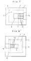
- the piezoelectric resonator has a cavity 2 provided by machining or etching in one side of a block of AT cut quartz crystal 1 centrally thereof to form a vibratory portion 3, which has a thickness of about 17 ⁇ m, if a fundamental resonance frequency of, say, 100 MHz is desired to obtain.
- the ultrathin vibratory portion 3 is edged with and mechanically supported by a thick frame-like marginal portion (or rib) 4 formed integrally therewith.
- a conductive film 5 all over the piezoelectric substrate on the side where the cavity 2 is provided and by depositing a partial electrode 6 and an electrode lead 7 extending therefrom, through use of, for example, vacuum evaporation on the flat surface of the vibratory portion 3 opposite from the cavity 2, it is possible to obtain a resonator of a very high resonance frequency substantially equal to the fundamantal resonant frequency of the ultrathin vibratory portion 3 or a filter element of such a high center frequency.
- the above-said piezoelectric resonator is suitable for housing in such a flat package as depicted in Fig. 2.
- the conductive film 10 on the bottom of the concavity of the case 8 is connected to a terminal 11 formed at one corner of the case 8 on the underside thereof via a connecting conductor hermetically passing through the case 8.
- a pad 7a at one end of the electrode lead 7 extending from the partial electrode 6 of the resonator has a minimum area necessary for connection, by a bonding wire 12, to a pad 14 formed on a stepped portion 13 on the inside of the case 8.
- the pad 14 is also connected to a terminal 15 provided at another corner of the case 8 on the underside thereof via a connecting conductor which hermetically passes through the case 8.
- the above-described ultrathin resonator studied so for has the overall electrode 5 on the side of the piezoelectric block (i.e.the piezoelectric plate) I where the cavity 2 is provided, and hence is easy to manufacture, but the overall electrode 5 and the electrode lead portion 7 extending from the partial electrode 6 are deposited on both sides of the ultrathin vibratory portion 3 and they constitute a capacitor of a large capacity, which causes an increase in a parallel capacitance C o in an equivalent circuit of the piezoelectric resonator shown in Fig. 3.
- VXO voltage controlled quartz crystal oscillator
- the present invention is intended to solve the above-mentioned problems of the ultrathin piezoelectric resonator which have been left unsolved so far, and it is an object of the invention to provide an electrode structure of an ultrathin piezoelectric resonator which is free from various drawbacks attributable to an increase in an equivalent parallel capacitance of the resonator which results from the formation of a capacitor between the overall electrode and the electrode lead portion deposited on both sides of the ultrathin vibratory portion forming the bottom of the cavity made in one side of a block of a piezoelectric material such as quartz crystal.
- the width (the sectional area) of the electrode lead portion 7 extending from the partial electrode 6 deposited opposite the overall electrode 5 on the bottom of the cavity of the piezoelectric plate 1 is selected large enough to make the ohmic loss(i.e. the electrode resistance) negligible, then a resonance is caused by the electrode lead portion 7 serving as a dummy electrode in the vicinity of the point of resonance by the afore mentioned true electrode and the resonance becomes a high-level spurious .
- JP-A-60 210018 discloses an ultrathin piezoelectric resonator wherein an overall electrode is provided over the entire area of one surface of a piezoelectric plate including an ultrathin vibratory portion and a surrounding thick frame-like marginal portion formed integrally therewith for supporting the vibratory portion; and a partial electrode and an electrode lead extending therefrom to one marginal edge of the piezoelectric plate are provided on the other surface of the piezoelectric plate and, according to the present invention, such a resonator is characterised in that the electrode lead comprises two or more narrow lead patterns.
- the ultrathin piezoelectric resonator employs the electrode structure which has the overall electrode deposited on the piezoelectric substrate on the side where the cavity is provided and the partial electrode on the opposite side therefrom.
- the partial electrode is formed on the vibratory portion in the cavity of the piezoelectric substrate and the narrow electrode lead which extends from the partial electrode climbing over the inner wall of the cavity and a stepped portion contiguous thereto, although the formation of the partial electrode and its lead portion can be carried out by a troublesome method which involves tilting the piezoelectric substrate during the vapor deposition, and in this instance it is not sure to secure the conduction of the electrode lead portion.
- the overall electrode is formed on the side where the cavity is provided.
- the resonator of this type is intended primarily for microminiaturization and it is desirable that the piezoelectric substrate has a size of 3 mm by 3mm or less, for example.
- the present invention utilizes a method by which a number of chips are formed on one piezoelectric wafer by batch processing and the wafer is cut into individual chips.
- the overall electrode can be formed simply by evaporating a conductive film all over one side of the wafer and no photomask or mask for photolithography is needed-this improves the efficiency of production, i.e. the yield rate of product, and hence affords reduction of manufacturing costs.
- the ultrathin piezoelectric resonator studied by the inventors so far has the overall electrode deposited on the substrate on the side where the cavity is formed.
- the vibratory portion is so thin that a large capacitance is formed between the overall electrode and the lead portion extending from the partial electrode deposited on opposite sides of the vibratory portion, and as a result, the capacitance ratio of the resonator becomes large, introducing various disadvantages.
- the width of the electrode lead portion 7 on the ultrathin vibratory portion 3 becomes about the same as the width of the partial electrode 6 as shown in Fig. 4, because the partial electrode 6 itself is very small.
- the overall electrode 5 and the electrode lead portion 7b deposited on both sides of vibratory portion 3 act as dummy electrodes and a spurious resonance of large level is caused by the electrode lead portion 7b in the vicinity of the point of resonance by the true electrode 6 as referred to previously.
- the ultrathin piezoelectric resonator according to the present invention uses such an electrode structure as described below.
- Fig. 5 is a plan view showing the basic structure of the present invention, wherein that portion of the electrode lead 7 extending from the partial electrode 6 deposited opposite the overall electrode 5 on the piezoelectric block 1 which lies on the ultrathin vibratory portion 3 is formed by a plurality of narrow electrode lead patterns 7c, 7c, ... in such a manner that the sum of their sectional areas may be sufficiently large enough to prevent an increase in the ohmic loss.
- the three electrode lead patterns 7c are extended from the partial electrode 6 to the pad 7a on the marginal portion of the piezoelectric block 1 but this is intended as being merely illustrative and the number of electrode lead patterns 7c may be two or more. Moreover, the electrode lead patterns need not always be parallel to each other.
- the area of the pad 7a can be set arbitrarily, because it lies on the thick frame-like marginal portion 4 and has nothing to do with the resonance of the vibratory portion 3 (even if it resonates, its resonance frequency is very lower than that of the resonance of the vibratory portion).
- the electrode structure of this embodiment is markedly effective in maintaining the spurious resonance characteristic of the easy-to-manufacture ultrathin piezoelectric resonator with the overall electrode deposited over one side of the piezoelectric block 1 without increasing its equivalent resistance.
- Fig. 6 shows an application of the electrode structure of Fig. 5 to the ultrathin piezoelectric block 1-including such unetched portions 20 and 22 as depicted in Figs. 8(a) and (b).
- unetched portions 20 and 22 are formed on the inner wall of the cavity 2 at a substantially constant angle of inclination in +x and -x directions, respectively, as shown in Fig.8 (a) . Consequently, the inner wall of the cavity 2 formed by etching does not form a vertical wall from the frame-like marginal portion 4 to the vibratory portion 3, but instead the unetched inclined portion of widths l 1 and l 2 are formed between the vibratory portion 3 and the frame-like marginal portion 4. These unetched portions meet the vibratory portion 3 at boundaries 21 and 23.
- the slope of the unetched portion 20 in the +x direction is gentler than the slope of the unetched portion 22 in the -x direction, that is, l 1 > l 2 .
- the electrode lead pattern 7 extending between the conductor pad 7a and the partial electrode 6 is narrow but is shortened by l 1 . This affords further reduction of the ohmic loss of the electrode lead portion 7 and permits holding low the capacitance between the electrode lead portion 7 and the overall electrode 5.
- the pad 7a lying on the frame-like marginal portion 4 is extended to the portion corresponding to the unetched portion 20 and the electrode lead portion 7 on the vibratory portion 3 is formed by a plurality of narrow electrode lead patterns 7b.
- the area of the electrode lead pattern 7b is shortend--this affords further reduction of the level of the spurious resonance by the electrode lead portion 7b and, at the same time, decreases the ohmic loss of the electrode lead portion and the equivalent parallel capacitance of the resonator.
- the ultrathin piezoelectric resonator is suitable for housing in, for example, a ceramic-sintered dish-like package such as shown in Fig. 2. That is, it is effective in simplifying the manufacturing process of the device to house the piezoelectric block 1 with the cavity 2 facing down toward the bottom of the package 8 and electrically connect and mechanically , fix the aluminum electrode film 5 on the frame-like marginal portion 4 of the block 1 and the aluminum film 10 on the bottom of the package 8 through use of the conductive adhesive 9.
- Fig. 7 shows an example of application of the embodiment of the present invention to a dual-mode filter. It is self evident that, also in the multimode filter element, if the ohmic loss of the electrode lead extending from each split electrode 19,19 is large, the insertion loss of the filter increases accordingly, and if the electrode lead is made wide, a spurious resonance is caused by the electrode lead in the vicinity of the passband of the filter, posing a problem that a desired attenuation cannot be obtained. In view of this, those portions of the electrode leads 17,17 extending from the split electrodes 19, 19 which are formed on the vibratory portion 3 are each formed by a plurality of narrow electrode lead patterns 17c as shown in Fig. 7.
- the area indicated by 16 in Fig. 7 is a blank area where the conductive film forming the overall electrode 5 is selectively removed from the area corresponding to the lead pattern 17c to form the blank area 16, thereby decreasing the parallel capacitance C o .
Landscapes
- Physics & Mathematics (AREA)
- Acoustics & Sound (AREA)
- Chemical & Material Sciences (AREA)
- Crystallography & Structural Chemistry (AREA)
- Piezo-Electric Or Mechanical Vibrators, Or Delay Or Filter Circuits (AREA)
Claims (3)
- Ultradünner piezoelektrischer Resonator, bei dem eine Gesamtelektrode (5) auf dem gesamten Bereich der einen Oberfläche einer piezoelektrischen Platte (1) vorgesehen ist, die einen ultradünnen Vibratorteil (3) und einen einstückig damit ausgebildeten und diesen umgebenden dicken rahmenartigen Randteil (4) zur Abstützung des Vibratorteils aufweist; und eine Partialelektrode (6) und eine Elektrodenzuleitung (7), die sich von jener bis zu der einen Randkante der piezoelektrischen Platte erstreckt, auf der anderen Oberfläche der piezoelektrischen Platte vorgesehen sind, dadurch gekennzeichnet, daß die Elektrodenzuleitung (7) zwei oder mehr schmale Zuleitungsmuster (7b, 7c, 17c) aufweist.
- Resonator nach Anspruch 1, bei dem ein breiter leitender Belag (7a) auf der anderen Oberfläche der piezoelektrischen Platte (1) in einem Bereich von ihrer einen Randkante (4) bis zu der Grenze (21) zwischen einer inneren Seitenwand (20) eines Hohlraums, der durch den rahmenartigen Randteil (4) begrenzt ist, und dem Vibratorteil vorgesehen ist; und der leitende Belag (7a) und die Partialelektrode (6) durch die schmalen Elektrodenzuleitungsmuster verbunden sind.
- Resonator nach Anspruch 2, bei dem die innere Seitenwand (20) allmählich zu dem Vibratorteil hin geneigt ist.
Applications Claiming Priority (11)
| Application Number | Priority Date | Filing Date | Title |
|---|---|---|---|
| JP13613490A JPH0435105A (ja) | 1990-05-25 | 1990-05-25 | 超薄板圧電共振子の電極構造 |
| JP136134/90 | 1990-05-25 | ||
| JP172114/90 | 1990-06-29 | ||
| JP02172114A JP3102872B2 (ja) | 1990-06-29 | 1990-06-29 | 超薄肉圧電振動子 |
| JP179577/90 | 1990-07-09 | ||
| JP17957790A JPH04181801A (ja) | 1990-07-09 | 1990-07-09 | 超薄板圧電共振子のリード構造 |
| JP23504190A JPH04115706A (ja) | 1990-09-05 | 1990-09-05 | 超薄板圧電共振子の電極リード構造 |
| JP23504290A JPH04115707A (ja) | 1990-09-05 | 1990-09-05 | 超薄板圧電共振子の電極リード構造 |
| JP235042/90 | 1990-09-05 | ||
| JP235041/90 | 1990-09-05 | ||
| PCT/JP1991/000615 WO1991019351A1 (fr) | 1990-05-25 | 1991-05-09 | Structure d'electrode et de sortie correspondante pour resonateur piezoelectrique a plaque mince |
Publications (3)
| Publication Number | Publication Date |
|---|---|
| EP0484545A1 EP0484545A1 (de) | 1992-05-13 |
| EP0484545A4 EP0484545A4 (en) | 1993-02-24 |
| EP0484545B1 true EP0484545B1 (de) | 1997-01-22 |
Family
ID=27527445
Family Applications (1)
| Application Number | Title | Priority Date | Filing Date |
|---|---|---|---|
| EP91908864A Expired - Lifetime EP0484545B1 (de) | 1990-05-25 | 1991-05-09 | Elektroden- und elektrodenleitungsstruktur eines piezoelektrischen resonators aus einer ultradünnen schicht |
Country Status (5)
| Country | Link |
|---|---|
| US (1) | US5235240A (de) |
| EP (1) | EP0484545B1 (de) |
| KR (1) | KR920702898A (de) |
| DE (1) | DE69124339T2 (de) |
| WO (1) | WO1991019351A1 (de) |
Cited By (1)
| Publication number | Priority date | Publication date | Assignee | Title |
|---|---|---|---|---|
| RU2234186C1 (ru) * | 2003-04-24 | 2004-08-10 | Мацак Андрей Николаевич | Высокочастотный пьезоэлемент |
Families Citing this family (21)
| Publication number | Priority date | Publication date | Assignee | Title |
|---|---|---|---|---|
| KR100363247B1 (ko) * | 1995-10-28 | 2003-02-14 | 삼성전자 주식회사 | 진동구조물및그것의고유진동수제어방법 |
| EP0818882A3 (de) * | 1996-07-10 | 1999-12-15 | Matsushita Electric Industrial Co., Ltd. | Piezoelektrische Vorrichtung mit eingefangener Energie und Herstellungsverfahren dazu |
| US6219531B1 (en) | 1998-09-04 | 2001-04-17 | Ericsson Inc. | Architecture and frequency plan for a UHF portable radio |
| DE19859172A1 (de) * | 1998-12-21 | 2000-06-29 | Uhp Corp | Selektive Oberflächenbehandlung durch magnetische Maskenhalterung |
| JP2001244778A (ja) * | 1999-12-22 | 2001-09-07 | Toyo Commun Equip Co Ltd | 高周波圧電振動子 |
| US6492759B1 (en) * | 2000-05-24 | 2002-12-10 | Toyo Communication Equipment Co., Ltd. | Piezoelectric resonator and a filter |
| US7098574B2 (en) * | 2002-11-08 | 2006-08-29 | Toyo Communication Equipment Co., Ltd. | Piezoelectric resonator and method for manufacturing the same |
| SE0300375D0 (sv) | 2003-02-12 | 2003-02-12 | Attana Ab | Piezoelectric resonator |
| US7126255B2 (en) * | 2004-04-05 | 2006-10-24 | Ngk Insulators, Ltd. | Piezoelectric/electrostrictive film-type device |
| CN101142742B (zh) * | 2005-04-18 | 2011-06-15 | 株式会社大真空 | 压电振动片和压电振动器件 |
| JP4629492B2 (ja) * | 2005-05-10 | 2011-02-09 | 太陽誘電株式会社 | 圧電薄膜共振子およびフィルタ |
| US7568377B2 (en) * | 2005-07-28 | 2009-08-04 | University Of South Florida | High frequency thickness shear mode acoustic wave sensor for gas and organic vapor detection |
| US20080169730A1 (en) * | 2007-01-11 | 2008-07-17 | Romi Mayder | Inverted mesa quartz crystal time base reference for automatic test equipment |
| CN102498666B (zh) * | 2009-09-18 | 2015-10-14 | 株式会社大真空 | 压电振动片以及压电振动片的制造方法 |
| GB201007349D0 (en) * | 2010-04-30 | 2010-06-16 | Cambridge Entpr Ltd | Antenna device |
| TW201251157A (en) | 2011-06-03 | 2012-12-16 | Seiko Epson Corp | Piezoelectric vibration element, manufacturing method for piezoelectric vibration element, piezoelectric vibrator, electronic device, and electronic apparatus |
| CN102957394B (zh) * | 2011-08-18 | 2016-12-21 | 精工爱普生株式会社 | 振动元件、振子、电子装置、电子设备、移动体及振动元件的制造方法 |
| US8970316B2 (en) | 2011-08-19 | 2015-03-03 | Seiko Epson Corporation | Resonating element, resonator, electronic device, electronic apparatus, and mobile object |
| US10352800B2 (en) | 2016-06-03 | 2019-07-16 | Mks Instruments, Inc. | Micromachined bulk acoustic wave resonator pressure sensor |
| DE102018131357A1 (de) * | 2018-12-07 | 2020-06-10 | Carl Freudenberg Kg | Sensorelement mit Befestigungsabschnitt |
| CN110880924A (zh) * | 2019-12-11 | 2020-03-13 | 武汉大学 | 一种可调谐的薄膜体声波谐振器 |
Family Cites Families (18)
| Publication number | Priority date | Publication date | Assignee | Title |
|---|---|---|---|---|
| US3694677A (en) * | 1971-03-03 | 1972-09-26 | Us Army | Vhf-uhf piezoelectric resonators |
| JPS5124351B2 (de) * | 1971-11-12 | 1976-07-23 | ||
| JPS5931889B2 (ja) * | 1976-10-18 | 1984-08-04 | セイコーインスツルメンツ株式会社 | 圧電振動子 |
| JPS5721114A (en) * | 1980-07-15 | 1982-02-03 | Citizen Watch Co Ltd | Electrode construction of quartz oscillator and its manufacture |
| JPS6318175Y2 (de) * | 1980-11-10 | 1988-05-23 | ||
| JPS58137318A (ja) * | 1982-02-10 | 1983-08-15 | Nec Corp | 薄膜圧電振動子 |
| JPS58157213A (ja) * | 1982-03-15 | 1983-09-19 | Toyo Commun Equip Co Ltd | チツプ振動子の構造及び製造方法 |
| FR2527865A1 (fr) * | 1982-06-01 | 1983-12-02 | Cepe | Resonateur piezo-electrique a haute frequence et son procede de fabrication |
| US4720651A (en) * | 1982-06-10 | 1988-01-19 | The United States Of America As Represented By The Secretary Of The Army | Resonator insensitive to paraxial accelerations |
| JPS5911520U (ja) * | 1982-07-13 | 1984-01-24 | 株式会社村田製作所 | 圧電共振部品 |
| JPS5931889A (ja) * | 1982-08-13 | 1984-02-21 | Nippon Kokan Kk <Nkk> | ニツケル−亜鉛合金メツキ鋼板の製造方法 |
| JPS59141813A (ja) * | 1983-02-02 | 1984-08-14 | Nec Corp | 薄膜圧電振動子 |
| FR2547458B3 (fr) * | 1983-06-07 | 1986-02-21 | Electronique Piezoelectricite | Resonateur piezoelectrique pourvu d'un dispositif d'encapsulation |
| JPS59195830U (ja) * | 1983-06-13 | 1984-12-26 | 東光株式会社 | 圧電振動子 |
| JPS60210018A (ja) * | 1984-04-03 | 1985-10-22 | Nec Corp | 薄膜圧電振動子 |
| JPS62185403A (ja) * | 1986-02-10 | 1987-08-13 | Fujitsu Ltd | 圧電振動子及びその製造方法 |
| JPS63144727A (ja) * | 1986-12-05 | 1988-06-16 | 積水化学工業株式会社 | 情報信号伝送用インタ−フエイスユニツト |
| JPS63144727U (de) * | 1987-03-13 | 1988-09-22 |
-
1991
- 1991-05-09 US US07/809,512 patent/US5235240A/en not_active Expired - Lifetime
- 1991-05-09 WO PCT/JP1991/000615 patent/WO1991019351A1/ja not_active Ceased
- 1991-05-09 EP EP91908864A patent/EP0484545B1/de not_active Expired - Lifetime
- 1991-05-09 DE DE69124339T patent/DE69124339T2/de not_active Expired - Fee Related
- 1991-07-25 KR KR1019910700781A patent/KR920702898A/ko not_active Ceased
Cited By (1)
| Publication number | Priority date | Publication date | Assignee | Title |
|---|---|---|---|---|
| RU2234186C1 (ru) * | 2003-04-24 | 2004-08-10 | Мацак Андрей Николаевич | Высокочастотный пьезоэлемент |
Also Published As
| Publication number | Publication date |
|---|---|
| KR920702898A (ko) | 1992-10-28 |
| EP0484545A1 (de) | 1992-05-13 |
| WO1991019351A1 (fr) | 1991-12-12 |
| DE69124339T2 (de) | 1997-05-15 |
| US5235240A (en) | 1993-08-10 |
| DE69124339D1 (de) | 1997-03-06 |
| EP0484545A4 (en) | 1993-02-24 |
Similar Documents
| Publication | Publication Date | Title |
|---|---|---|
| EP0484545B1 (de) | Elektroden- und elektrodenleitungsstruktur eines piezoelektrischen resonators aus einer ultradünnen schicht | |
| EP1478090B1 (de) | Piezoelektrisches Stimmgabel-Resonatorbauelement | |
| US6111480A (en) | Piezoelectric resonator and method of adjusting resonant frequency thereof | |
| EP0641073B1 (de) | Eingekapselter piezoelektrischer Resonator | |
| US5925968A (en) | Piezoelectric vibrator, piezoelectric vibrator device having the same and circuit device having the piezoelectric vibrator device | |
| JP3229336B2 (ja) | 表面がマイクロ機械加工された音響波ピエゾ電気結晶 | |
| EP0483358B1 (de) | Ultradünne quartzkristallfiltereinheit mit mehreren moden | |
| JP2004200777A (ja) | メサ構造の圧電基板、圧電振動素子、圧電振動子、及び圧電発振器 | |
| EP0468051B1 (de) | Struktur eines piezoelektrischen resonators aus einer ultradünnen schicht | |
| JP4196641B2 (ja) | 超薄板圧電デバイスとその製造方法 | |
| JP6439808B2 (ja) | 音叉型振動子 | |
| JP2001257560A (ja) | 超薄板圧電振動素子の電極構造 | |
| JP3277501B2 (ja) | 圧電共振子の構造及びその製造方法 | |
| JP3102872B2 (ja) | 超薄肉圧電振動子 | |
| JP2026061960A (ja) | 水晶デバイス、水晶振動片及び水晶ウエハ | |
| KR20030054244A (ko) | 칩형 공진기 및 그 제조방법 | |
| JP7725963B2 (ja) | 水晶振動板および水晶振動デバイス | |
| JP6708224B2 (ja) | 音叉型振動子の製造方法 | |
| JPH04115707A (ja) | 超薄板圧電共振子の電極リード構造 | |
| JPH04115706A (ja) | 超薄板圧電共振子の電極リード構造 | |
| JPH0435105A (ja) | 超薄板圧電共振子の電極構造 | |
| KR940009397B1 (ko) | 초박판 다중모드 수정필터소자 | |
| JP2026061961A (ja) | 水晶デバイス、水晶振動片及び水晶ウエハ | |
| JP2001060844A (ja) | 複合圧電振動子 | |
| JP2007189579A (ja) | 圧電基板の製造方法、圧電基板、圧電振動素子、超薄板多重モード圧電フィルタ素子、圧電振動素子の製造方法、圧電振動子、及び圧電発振器 |
Legal Events
| Date | Code | Title | Description |
|---|---|---|---|
| PUAI | Public reference made under article 153(3) epc to a published international application that has entered the european phase |
Free format text: ORIGINAL CODE: 0009012 |
|
| 17P | Request for examination filed |
Effective date: 19920220 |
|
| AK | Designated contracting states |
Kind code of ref document: A1 Designated state(s): DE FR GB |
|
| A4 | Supplementary search report drawn up and despatched |
Effective date: 19930106 |
|
| AK | Designated contracting states |
Kind code of ref document: A4 Designated state(s): DE FR GB |
|
| 17Q | First examination report despatched |
Effective date: 19950504 |
|
| GRAG | Despatch of communication of intention to grant |
Free format text: ORIGINAL CODE: EPIDOS AGRA |
|
| GRAH | Despatch of communication of intention to grant a patent |
Free format text: ORIGINAL CODE: EPIDOS IGRA |
|
| GRAH | Despatch of communication of intention to grant a patent |
Free format text: ORIGINAL CODE: EPIDOS IGRA |
|
| GRAA | (expected) grant |
Free format text: ORIGINAL CODE: 0009210 |
|
| AK | Designated contracting states |
Kind code of ref document: B1 Designated state(s): DE FR GB |
|
| ET | Fr: translation filed | ||
| REF | Corresponds to: |
Ref document number: 69124339 Country of ref document: DE Date of ref document: 19970306 |
|
| PLBE | No opposition filed within time limit |
Free format text: ORIGINAL CODE: 0009261 |
|
| STAA | Information on the status of an ep patent application or granted ep patent |
Free format text: STATUS: NO OPPOSITION FILED WITHIN TIME LIMIT |
|
| 26N | No opposition filed | ||
| REG | Reference to a national code |
Ref country code: GB Ref legal event code: IF02 |
|
| PGFP | Annual fee paid to national office [announced via postgrant information from national office to epo] |
Ref country code: GB Payment date: 20040512 Year of fee payment: 14 |
|
| PGFP | Annual fee paid to national office [announced via postgrant information from national office to epo] |
Ref country code: DE Payment date: 20040520 Year of fee payment: 14 |
|
| PGFP | Annual fee paid to national office [announced via postgrant information from national office to epo] |
Ref country code: FR Payment date: 20040528 Year of fee payment: 14 |
|
| PG25 | Lapsed in a contracting state [announced via postgrant information from national office to epo] |
Ref country code: GB Free format text: LAPSE BECAUSE OF NON-PAYMENT OF DUE FEES Effective date: 20050509 |
|
| PG25 | Lapsed in a contracting state [announced via postgrant information from national office to epo] |
Ref country code: DE Free format text: LAPSE BECAUSE OF NON-PAYMENT OF DUE FEES Effective date: 20051201 |
|
| GBPC | Gb: european patent ceased through non-payment of renewal fee |
Effective date: 20050509 |
|
| PG25 | Lapsed in a contracting state [announced via postgrant information from national office to epo] |
Ref country code: FR Free format text: LAPSE BECAUSE OF NON-PAYMENT OF DUE FEES Effective date: 20060131 |
|
| REG | Reference to a national code |
Ref country code: FR Ref legal event code: ST Effective date: 20060131 |