EP0484982A2 - Elektronisches Gerät mit steuerbarer Stromversorgung - Google Patents
Elektronisches Gerät mit steuerbarer Stromversorgung Download PDFInfo
- Publication number
- EP0484982A2 EP0484982A2 EP91119096A EP91119096A EP0484982A2 EP 0484982 A2 EP0484982 A2 EP 0484982A2 EP 91119096 A EP91119096 A EP 91119096A EP 91119096 A EP91119096 A EP 91119096A EP 0484982 A2 EP0484982 A2 EP 0484982A2
- Authority
- EP
- European Patent Office
- Prior art keywords
- voltage
- switch
- response
- electronic apparatus
- output
- Prior art date
- Legal status (The legal status is an assumption and is not a legal conclusion. Google has not performed a legal analysis and makes no representation as to the accuracy of the status listed.)
- Granted
Links
Images





Classifications
-
- G—PHYSICS
- G06—COMPUTING OR CALCULATING; COUNTING
- G06F—ELECTRIC DIGITAL DATA PROCESSING
- G06F1/00—Details not covered by groups G06F3/00 - G06F13/00 and G06F21/00
- G06F1/26—Power supply means, e.g. regulation thereof
- G06F1/30—Means for acting in the event of power-supply failure or interruption, e.g. power-supply fluctuations
Definitions
- the present invention relates to measures to be taken in an electronic apparatus having a battery as a power supply when the battery voltage falls.
- method 2) needs an input port for monitoring the battery voltage which is sometimes difficult to realize the comparison circuit in a single chip microcomputer since the number of ports of the microcomputer may not be sufficient.
- an apparatus using a memory card or the like needs some input ports to monitor the state of predetermined signals of a bus between the battery and the card when memory protection is performed in accordance with the state of the battery, and such an apparatus is difficult to design.
- the invention is directed to electronic apparatus having a controllable power supply in which the power supply is controlled according to the operational state of a power on switch and a power off switch.
- the same control state as that in which the power off switch is actuated is produced upon detection that the power supply output falls below a first predetermined value and the operation of the power on switch is inhibited upon detection that the power supply output falls below a second predetermined value.
- An electronic apparatus of the present invention is driven by a battery and has a plurality of IC cards as external storage means, at least a keyboard as a user interface means and a display.
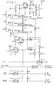
- Fig. 1 shows a power supply portion and a circuit for performing control operations based on the detection of the supply voltage in the electronic apparatus.
- BATT1, BATT2 and REG designate a battery serving as a power supply, a backup battery for a RAM, and a voltage regulator, respectively.
- the regulator REG is composed of a well-known integrated circuit and so on, stabilizes an output voltage of the battery BATT1, and outputs a fixed voltage VDD1.
- Schottky barrier diodes D1 and D2 apply one of the VDD1 and the voltage of the battery BATT2 to generate a battery voltage VDD2.
- the battery voltage VDD2 is supplied as a battery voltage of the circuit shown in Fig. 1 and a battery voltage of ic2 shown in Fig. 4.
- Slide switches SW1, SW2 and SW3 are a battery replacement switch, an IC card 1 replacement switch, and an IC card 2 replacement switch, respectively. These switches are operated in mechanical relation to the replacement of the battery and the IC cards (or manual manipulation) and are shown positioned to the left in the figure.
- Ic5 (ic5-1 to ic5-3) is a Schmitt-input NAND circuit to detect the operation states of the slide switches SW1, SW2 and SW3.
- Ic6 (ic6-1 to ic6-3) and ic7 (ic7-1 to ic7-4) are a NOR circuit and an analog switch, respectively.
- Voltage detectors DET1 and DET2 each output a signal of 'L' level from a Vo terminal when the battery voltage VDD2 is lowered.
- the relation between detected voltages VDET1 and VDET2 of the voltage detectors DET1 and DET2 is VDET1 > VDET2.
- Ic5-1 outputs a signal of 'L' level to ic6-1 and ic6-2 only when both the switches SW2 and SW3 (the IC card replacement switches) are positioned to the left in the figure.
- Ic5-2 and ic5-3 invert and transmit outputs of the voltage detectors DET1 and DET2 to ic6-1 and ic6-2 only when the switch SW1 (the battery replacement switch) is positioned to the left in the figure.
- Ic6-1 and ic6-2 each output a signal of 'L' level only when outputs of both ic5-1 and ic5-3 are of 'H' level.
- Ic6-2 controls the analog switch ic7-2 in response to the output.
- Ic6-3 generates a signal obtained by inverting the output of ic6-1, and controls the analog switch ic7-1 in response to the signal.
- the analog switches ic7-3 and ic7-4 are directly controlled by the output of the voltage detector DET2.
- the analog switch ic7-1 is placed so as to connect a key strobe signal KS1 and a key input signal Ki0 (a key matrix will be specifically described below in reference to Fig. 2).
- the analog switch ic7-1 is forced into the same state as that in which an OFF key disposed between the key strobe signal KS1 and the key input signal Ki0 is pressed down.
- the analog switch ic7-2 controls the connection of key strobe signals KS0 between a CPU and a key matrix, and prohibits the input of an ON key.
- CS9 negative logic
- a 'L' level input high impedance state
- C1, C2, C10, C11, C17, C18 and C19 each designate a bypass capacitor
- R2 designates a current limiting resistor
- C12, C13, C14, C15 and C16 each designate a noise absorption bypass capacitor
- R6 and R7 each designate a pull-up resistor.
- Fig. 2 shows a key matrix KM of the electronic apparatus of the present invention.
- Ki0 to Ki6 each denote a key input (scan) signal
- KS0 to KS11 each denote a key strobe signal.
- the ON key is placed at an intersection of a key strobe signal key KS0 and a key input signal key KiO, and the OFF key is placed at an intersection of a key KS1 and a key KiO.
- These ON and OFF keys are used to control ON/OFF of the main power supply.
- the ON key also has a function of displaying a predetermined menu.
- Fig. 3 shows a display circuit of the electronic apparatus of the present invention.
- ic20, ic21 and ic22, Disp, C20 to C30, and R20 designate a common driver for an LCD, LCD segment drivers, an LCD display, bypass capacitors, and a resistor for controlling the oscillation of the common driver ic20.
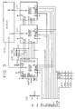
- Fig. 4 shows a CPU and a memory circuit of the electronic apparatus of the present invention.
- a CPU ic1 controls the execution of processes of the electronic apparatus, and a RAM ic2 functions as a memory for data storage and work of the CPU.
- ROMs ic3 and ic4 store a process program to be executed by the CPU ic1 and data for reference.
- XTAL, C1 and C2, R1, R8, and C6, C7, C8 and C9 designate an oscillator for generating operational clocks for the CPU ic1, capacitors for compensating the phase of the clocks, a damping resistor, a pull-up resistor, and bypass capacitors, respectively.
- C3, CN1 and CN2 designate a time constant capacitor for generating a reset signal of the electronic apparatus, a connector for the IC card 1, and a connector for the IC card 2.
- KM represents the key matrix shown in Fig. 2.
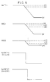
- Figs. 5 and 6 each show the timing of main signals on the circuit shown in Fig. 1.
- the supply voltage VDD1 is set at a fixed voltage of 5V by the regulator REG.
- the supply voltage VDD2 through the diode D1 is 4.7V which is approximately 0.3V lower than the supply voltage VDD1.
- Outputs of both the detectors DET1 and DET2 are of 'H' level.
- VDD1 When the voltage VDD1 is lowered to approximately 4.5V, each ic shown in Figs. 3 and 4 reaches the lower limit of the operational voltage guaranteed by the manufacturer. At this time, VDD2 is approximately 4.2V and the output of the detector DET1 is set to 'L' level.
- the output of the detector DET2 is also set to 'L' level.
- Fig. 6 shows the relationships between the switches SW1 to SW3 and the DET1, and between the DET2 and control signals of ic7-1 to 7-3.
- the display Disp performs display operations under the control of the drivers ic20, ic21 and ic22, and stops the display operations and goes into the standby state (ultra low current consumption mode) when a 'L' level input is applied as an STB signal from the CPU (ic1) shown in Fig. 4.
- Fig. 4 the processes to be carried out by ic1 are stored in ic3 or ic4.
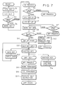
- Fig. 7 is a flow chart of one of the processes.
- WORK in the flow chart denotes a predetermined area of the RAM ic2, and I/O means an electronic circuit built in the CPU ic1 and the display circuit shown in Fig. 3.
- Step S1 the register in the CPU and the interruption mode axe initialized.
- Step S2 the circuit I/O built in the CPU and the display circuit shown in Fig. 3 are initialized.
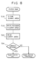
- Step S3 it is checked whether or not the RAM can normally perform the access. If the RAM is normal(good), Step S4 is executed, and if the RAM is not normal (wrong), a reset operation is repeated in Step S1.
- a predetermined area (several bytes) of the RAM is secured as a dummy area, and it is checked whether or not normal access to the dummy area of the RAM is possible.
- Step S31 the whole dummy area is cleared.
- Step S32 a predetermined message (for example, the name of the manufacturer or the name of the software) is written in the dummy area.
- Step S33 the dummy area is read.
- Step S34 it is determined whether or not the read data accords with the written data. If both the data are the same, it is determined that the RAM is normal. If the data do not agree, it is determined that there is something wrong in the RAM.
- Step S4 the work area of the RAM is initialized in Step S4.
- Step S5 the RAM is checked in the same manner as in Step S3. If the RAM is not normal, an OFF process is executed, and if the RAM is normal, Step S6 is executed.
- Step S6 A set-up process of the CPU, for example, the minimum initialization of the register, is carried out.
- Step S7 a set-up process of the circuit I/O, the minimum initialization of the circuit I/O or the return to the state immediately before the OFF state of the circuit I/O is executed and Step S7' is executed.
- the RAM is checked in Step S7' in the same manner as above.
- Step S8 the work area of the RAM is initialized to a minimum.
- Step S9 the OFF key is scanned. If the OFF key is pressed, Step S10 is executed, and if the OFF key is not pressed, Step S11 is executed.
- the press-down state of the OFF key is obtained through the analog switch ic7-1 not only when the OFF key is actually pressed down, but also when the supply voltage drops below 3.5V as described above, and when the IC card or the battery is replaced.
- Step S10 a message for indicating that the battery is running low (for example, "Low battery!) is displayed for approximately two seconds in Step S10 and the OFF process is executed.
- Step S11 a set-up image is displayed.
- Step S12 a wait for the key input by the key matrix shown in Fig. 2 is initiated. If the data key is pressed, Step S13 is executed, if one of keys other than the OFF key is pressed, Step S14 is executed, and if the OFF key is pressed, Step S15 is executed.
- Step S13 a data input process is performed and a wait for the key input in Step S12 is repeated.
- Step S14 a process corresponding to the pressed key other than the data key and the OFF key is performed.
- Step S15 a terminate process (end process: process previous to OFF state) of the work area of the RAM is executed.
- Step S16 the terminate process of the circuit I/O is executed, and Step S17 is executed.
- Step S17 an interrupt enable operation of the CPU is performed and a halt instruction is executed, thereby putting the apparatus into the OFF state.
- the OFF state of the apparatus of the present invention means the state in which the CPU stops the generation of clocks and goes into the standby state (ultra low current consumption mode), the STB signal of the display circuit shown in Fig. 3 is turned to 'L' and the display circuit is on standby.
- Step S5 the processes subsequent to Step S5 are executed again.
- the configuration of the apparatus is simpler than the conventional one in which the CPU detects the voltage by using the input port.
- the replacement of the IC card and the batteries is detected by the switches SW1 to SW3, the ON and OFF keys are controlled in accordance with the replacement, and the RAM can be reliably and easily protected.
- the RAM Since the access state of the memory is checked in the reset process when the system is started, and the reset process is repeated until the normal access becomes possible, even if the battery voltage is lowered, the RAM can be certainly protected and incorrect operations of the system due to the protection of the RAM can be prevented by replacing the battery, thereby making protection of the RAM extremely easy and inexpensive.
- the protection process can be executed by controlling the operational state of the ON and OFF keys even if there is an output from the switch operated when the IC card or the battery is replaced (switches other than the illustrated slide switch may be used), the protection of the memory during the replacement can be certainly achieved, thus preventing incorrect operations of the apparatus.
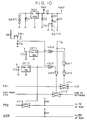
- Figs. 9 and 10 are variations of the above configuration of the electronic apparatus.
- analog switches ic7-3 and ic7-4 for protecting the RAM are directly controlled by the output of the detector DET2 in the above description, there is provided a detector DET3 for detecting the battery voltage VDD2 in order to control the analog switches ic7-3 and 7-4 in Fig. 9.
- the other components are the same as those shown in Fig. 1.
- VDET1 VDET2 > VDET3.
- a slide switch for replacement of the IC card is used in the above embodiment, such a switch is not always in an electronic apparatus which is not an IC card.
- An embodiment in which the slide switch is omitted is shown in Fig. 10.
- control of the battery voltage by the voltage detectors DET1 and DET2 and the control when the battery is replaced are performed in the same manner as above.
- the correlation of the input and output data in a predetermined address may be performed by repeating pushing down and popping up the data to and from the stack as shown in Fig. 11.
- Step S51 shown in Fig. 11 a predetermined counter register is set at the maximum number (in the case that msb to lsb of one word or one byte as a unit to be pushed/popped is 1), and the contents of the counter register are pushed down/popped up in Steps S52 and S53. At this time, a stack pointer is controlled to point a predetermined address to be checked. The popped data is stored in an accumulator.
- Step S54 the contents of the accumulator and the counter register are correlated. If the contents do not agree, it is determined that an error occurred in the memory and the reset process is executed.
- Step S55 The number of the counter register is decreased in Step S55, and it is checked in Step S56 whether or not the number reaches 0. If the number is not 0, the processes subsequent to Step S52 are repeated.
- an electronic apparatus which executes a predetermined protection process when the supply voltage falls below a predetermined voltage, includes a control for controlling a power supply of the apparatus in accordance with the operational state of a power on switch and a power off switch, a first detector for detecting that the supply voltage falls below a first predetermined voltage, a second detector for detecting that the supply voltage falls below a second predetermined voltage lower than the first predetermined voltage, and hardware for producing the same control state as that in which the power off switch is actuated in response to the detection output of the first detector and prohibiting the operation and input of the power on switch in response to the detection output of the second detector.
- a protection process can be performed by detecting the supply voltage with respect to the two predetermined voltages, and forming the same state as that in which the power on or off switch is put into a predetermined condition in accordance with the detection result. Furthermore, the protection process when the battery voltage falls can be simplified and reliably and easily executed. By using unregulated voltage detectors, the production and operation efficiency is greatly improved, and any special input port which is used in conventional CPU software is unnecessary. In addition, it is possible to produce an apparatus at relatively lower cost than that of the apparatus using a reset IC.
- the power supply of electronic apparatus is controlled according to the operational state of a power on switch and a power off switch.
- a first detector detects that the power supply voltage falls below a first predetermined voltage and a second detector detects that the power supply voltage falls below a second predetermined voltage.
- a device produces the same operational state as that in which the power off switch is actuated in response to the detection output of the first detector and prohibits the operation of the power on switch in response to the detection output of the second detector.
- a predetermined protection process is performed when the power supply voltage falls below a prescribed voltage in which the supply voltage is compared with the two predetermined voltages to produce the same state as when the power on or the power off switch is put into a predetermined condition in response to the comparison result.
Landscapes
- Engineering & Computer Science (AREA)
- Theoretical Computer Science (AREA)
- Physics & Mathematics (AREA)
- General Engineering & Computer Science (AREA)
- General Physics & Mathematics (AREA)
- Power Sources (AREA)
- Direct Current Feeding And Distribution (AREA)
Applications Claiming Priority (3)
| Application Number | Priority Date | Filing Date | Title |
|---|---|---|---|
| JP30267590 | 1990-11-09 | ||
| JP302675/90 | 1990-11-09 | ||
| JP2302675A JPH04178114A (ja) | 1990-11-09 | 1990-11-09 | 電子機器 |
Publications (3)
| Publication Number | Publication Date |
|---|---|
| EP0484982A2 true EP0484982A2 (de) | 1992-05-13 |
| EP0484982A3 EP0484982A3 (en) | 1994-08-24 |
| EP0484982B1 EP0484982B1 (de) | 1999-06-23 |
Family
ID=17911835
Family Applications (1)
| Application Number | Title | Priority Date | Filing Date |
|---|---|---|---|
| EP91119096A Expired - Lifetime EP0484982B1 (de) | 1990-11-09 | 1991-11-08 | Elektronisches Gerät mit steuerbarer Stromversorgung |
Country Status (4)
| Country | Link |
|---|---|
| US (1) | US5546589A (de) |
| EP (1) | EP0484982B1 (de) |
| JP (1) | JPH04178114A (de) |
| DE (1) | DE69131372T2 (de) |
Families Citing this family (17)
| Publication number | Priority date | Publication date | Assignee | Title |
|---|---|---|---|---|
| JP2983111B2 (ja) * | 1992-07-20 | 1999-11-29 | 富士通株式会社 | 電気機器装置 |
| JP2892963B2 (ja) * | 1995-02-28 | 1999-05-17 | キヤノン株式会社 | バッテリ駆動型コンピュータ |
| US5802379A (en) * | 1995-08-24 | 1998-09-01 | Norand Corporation | Battery depletion management in portable computing devices having PCMCIA card loading |
| JP3122605B2 (ja) * | 1995-11-17 | 2001-01-09 | シャープ株式会社 | 電子機器 |
| US5991887A (en) * | 1996-02-28 | 1999-11-23 | Dallas Semiconductor Corporation | Low power wake up circuitry, with internal power down of the wake up circuitry itself |
| KR100278355B1 (ko) * | 1996-09-30 | 2001-01-15 | 윤종용 | 컴퓨터 시스템 및 이 컴퓨터 시스템의 제어 방법 |
| US5884084A (en) * | 1996-10-31 | 1999-03-16 | Intel Corporation | Circuit and method for using early reset to prevent CMOS corruption with advanced power supplies |
| KR100186349B1 (en) * | 1996-12-17 | 1999-04-15 | Lg Ind Systems Co Ltd | Power failure compensation method of plc and plc having function of power failure compensation |
| JP2000010666A (ja) * | 1998-06-19 | 2000-01-14 | Toshiba Corp | コンピュータシステムおよびフラッシュrom書き換え方法 |
| JP2001250092A (ja) * | 2000-03-03 | 2001-09-14 | Toshiba Corp | カード型電子機器、及びカード型電子機器に適用されるコンテンツ管理方法 |
| JP2004164204A (ja) * | 2002-11-12 | 2004-06-10 | Toshiba Corp | 電子機器 |
| KR100605820B1 (ko) * | 2004-03-22 | 2006-08-01 | 삼성전자주식회사 | 피디에이 기능과 폰 기능을 구비한 피디에이폰에서사용자데이터 보호방법 |
| US20060242458A1 (en) * | 2005-03-31 | 2006-10-26 | Daniel Feldman | Computer volatile memory power backup system |
| CN101398710B (zh) * | 2007-09-27 | 2011-07-27 | 鸿富锦精密工业(深圳)有限公司 | 主板供电电路 |
| CN101556497B (zh) * | 2008-04-09 | 2011-06-22 | 鸿富锦精密工业(深圳)有限公司 | 主板供电电路 |
| KR101161994B1 (ko) * | 2010-12-03 | 2012-07-03 | 에스케이하이닉스 주식회사 | 멀티 칩 패키지 장치 및 그의 동작 방법 |
| KR102347602B1 (ko) * | 2017-08-28 | 2022-01-05 | 삼성전자주식회사 | 반도체 장치 및 그 파워 오프 방법 |
Family Cites Families (21)
| Publication number | Priority date | Publication date | Assignee | Title |
|---|---|---|---|---|
| FR638867A (fr) * | 1926-12-23 | 1928-06-05 | Propulseur hydro-pneumatique à l'usage de la navigation maritime | |
| US4096560A (en) * | 1977-10-28 | 1978-06-20 | Rockwell International Corporation | Protection circuit to minimize the effects of power line interruptions on the contents of a volatile electronic memory |
| JPS56162122A (en) * | 1980-05-16 | 1981-12-12 | Canon Inc | Electronic apparatus equipped with printing device |
| JPS57148726A (en) * | 1981-03-12 | 1982-09-14 | Nippon Kogaku Kk <Nikon> | Camera |
| US4422163A (en) * | 1981-09-03 | 1983-12-20 | Vend-A-Copy, Inc. | Power down circuit for data protection in a microprocessor-based system |
| DE3373759D1 (en) * | 1982-06-09 | 1987-10-22 | Fujitsu Ltd | One-chip semiconductor device incorporating a power-supply-potential detecting circuit with reset function |
| US4645326A (en) * | 1984-03-30 | 1987-02-24 | Canon Kabushiki Kaisha | Camera with computer circuit |
| US4766567A (en) * | 1984-04-19 | 1988-08-23 | Ltd. Nippondenso Co. | One-chip data processing device including low voltage detector |
| US4777626A (en) * | 1984-12-22 | 1988-10-11 | Tokyo Electric Co., Ltd. | Memory device having backup power supply |
| JPH0833790B2 (ja) * | 1986-12-26 | 1996-03-29 | 株式会社東芝 | コンピユ−タにおける電源遮断装置 |
| JP2526572B2 (ja) * | 1987-03-20 | 1996-08-21 | 株式会社精工舎 | カメラ用電源回路 |
| US5053804A (en) * | 1987-07-10 | 1991-10-01 | Canon Kabushiki Kaisha | Camera having computer |
| US5157270A (en) * | 1987-10-31 | 1992-10-20 | Canon Kabushiki Kaisha | Reset signal generating circuit |
| JP2533612B2 (ja) * | 1988-05-16 | 1996-09-11 | 富士通株式会社 | メモリのデ―タ保護方式 |
| FR2638867A1 (fr) * | 1988-11-04 | 1990-05-11 | Sgs Thomson Microelectronics | Procede et circuit de reinitialisation du fonctionnement d'un circuit |
| US5349669A (en) * | 1988-12-21 | 1994-09-20 | Oki Electric Industry Co., Ltd. | Data write control means |
| US5218607A (en) * | 1989-06-23 | 1993-06-08 | Kabushiki Kaisha Toshiba | Computer having a resume function and operable on an internal power source |
| US5079583A (en) * | 1989-08-31 | 1992-01-07 | Canon Kabushiki Kaisha | Shutter apparatus which also serves as a diaphragm |
| US5243577A (en) * | 1989-12-11 | 1993-09-07 | Sharp Kabushiki Kaisha | Electronic apparatus |
| JPH04109547A (ja) * | 1990-08-30 | 1992-04-10 | Sharp Corp | メモリデータ保護装置 |
| US5237698A (en) * | 1991-12-03 | 1993-08-17 | Rohm Co., Ltd. | Microcomputer |
-
1990
- 1990-11-09 JP JP2302675A patent/JPH04178114A/ja active Pending
-
1991
- 1991-11-08 EP EP91119096A patent/EP0484982B1/de not_active Expired - Lifetime
- 1991-11-08 DE DE69131372T patent/DE69131372T2/de not_active Expired - Fee Related
-
1995
- 1995-02-13 US US08/387,621 patent/US5546589A/en not_active Expired - Fee Related
Also Published As
| Publication number | Publication date |
|---|---|
| EP0484982A3 (en) | 1994-08-24 |
| DE69131372D1 (de) | 1999-07-29 |
| JPH04178114A (ja) | 1992-06-25 |
| DE69131372T2 (de) | 2000-03-23 |
| EP0484982B1 (de) | 1999-06-23 |
| US5546589A (en) | 1996-08-13 |
Similar Documents
| Publication | Publication Date | Title |
|---|---|---|
| US5546589A (en) | System having controlled power supply for prohibiting the power on switch from being turned on and accessing memory when supply voltage falls below second predetermined voltage | |
| US5311441A (en) | Battery powered unit with battery sensor and resume processing control means | |
| KR100395131B1 (ko) | 스마트 배터리의 실제 잔류 용량을 표시하기 위한 장치 및방법 | |
| US5375246A (en) | Back-up power supply apparatus for protection of stored data | |
| US5475271A (en) | Power source control system for electronic device and expansion unit connected thereto | |
| US5969529A (en) | Electronic apparatus having battery power source | |
| KR930004943B1 (ko) | 리쥼 기능을 갖는 컴퓨터 | |
| US5991839A (en) | Computer system having computer main body and expansion unit | |
| US5875345A (en) | Information processing system having dual power saving modes | |
| US5341316A (en) | Personal computer system allowing selective use of built-in and external keyboards by means of selector | |
| US5440603A (en) | Watch-dog timer circuit and a microcomputer equipped therewith | |
| US5479645A (en) | Portable computer capable of switching CPU clocks | |
| US5410712A (en) | Computer system equipped with extended unit including power supply | |
| US6772366B2 (en) | Method and apparatus for detecting AC removal | |
| US20030154230A1 (en) | Electronic device and camera | |
| US4849919A (en) | System wake up circuit for computer | |
| US6567868B1 (en) | Structure and method for automatically setting the CPU speed | |
| US6647475B2 (en) | Processor capable of enabling/disabling memory access | |
| JP3404664B2 (ja) | 端末装置 | |
| EP0482527A2 (de) | System zur Schaltsteuerung zwischen Normal und Ersatz | |
| JP2951959B2 (ja) | 制御回路のデータ保護方法 | |
| JP2002359931A (ja) | 電子機器、その制御方法、及びその制御プログラムを格納したコンピュータにより読み取り可能な記憶媒体 | |
| JP2001157361A (ja) | 回路装置およびデータ管理方法 | |
| JPS6411978B2 (de) | ||
| JPS62259121A (ja) | 1チツプcpuの電源装置 |
Legal Events
| Date | Code | Title | Description |
|---|---|---|---|
| PUAI | Public reference made under article 153(3) epc to a published international application that has entered the european phase |
Free format text: ORIGINAL CODE: 0009012 |
|
| AK | Designated contracting states |
Kind code of ref document: A2 Designated state(s): DE ES FR GB IT |
|
| PUAL | Search report despatched |
Free format text: ORIGINAL CODE: 0009013 |
|
| AK | Designated contracting states |
Kind code of ref document: A3 Designated state(s): DE ES FR GB IT |
|
| 17P | Request for examination filed |
Effective date: 19950110 |
|
| 17Q | First examination report despatched |
Effective date: 19950725 |
|
| GRAG | Despatch of communication of intention to grant |
Free format text: ORIGINAL CODE: EPIDOS AGRA |
|
| GRAG | Despatch of communication of intention to grant |
Free format text: ORIGINAL CODE: EPIDOS AGRA |
|
| GRAH | Despatch of communication of intention to grant a patent |
Free format text: ORIGINAL CODE: EPIDOS IGRA |
|
| GRAH | Despatch of communication of intention to grant a patent |
Free format text: ORIGINAL CODE: EPIDOS IGRA |
|
| GRAA | (expected) grant |
Free format text: ORIGINAL CODE: 0009210 |
|
| AK | Designated contracting states |
Kind code of ref document: B1 Designated state(s): DE ES FR GB IT |
|
| PG25 | Lapsed in a contracting state [announced via postgrant information from national office to epo] |
Ref country code: IT Free format text: LAPSE BECAUSE OF FAILURE TO SUBMIT A TRANSLATION OF THE DESCRIPTION OR TO PAY THE FEE WITHIN THE PRE;WARNING: LAPSES OF ITALIAN PATENTS WITH EFFECTIVE DATE BEFORE 2007 MAY HAVE OCCURRED AT ANY TIME BEFORE 2007. THE CORRECT EFFECTIVE DATE MAY BE DIFFERENT FROM THE ONE RECORDED.SCRIBED TIME-LIMIT Effective date: 19990623 Ref country code: ES Free format text: THE PATENT HAS BEEN ANNULLED BY A DECISION OF A NATIONAL AUTHORITY Effective date: 19990623 |
|
| REF | Corresponds to: |
Ref document number: 69131372 Country of ref document: DE Date of ref document: 19990729 |
|
| ET | Fr: translation filed | ||
| PLBE | No opposition filed within time limit |
Free format text: ORIGINAL CODE: 0009261 |
|
| 26N | No opposition filed | ||
| REG | Reference to a national code |
Ref country code: GB Ref legal event code: IF02 |
|
| PGFP | Annual fee paid to national office [announced via postgrant information from national office to epo] |
Ref country code: GB Payment date: 20031105 Year of fee payment: 13 |
|
| PGFP | Annual fee paid to national office [announced via postgrant information from national office to epo] |
Ref country code: FR Payment date: 20031110 Year of fee payment: 13 |
|
| PGFP | Annual fee paid to national office [announced via postgrant information from national office to epo] |
Ref country code: DE Payment date: 20031120 Year of fee payment: 13 |
|
| PG25 | Lapsed in a contracting state [announced via postgrant information from national office to epo] |
Ref country code: GB Free format text: LAPSE BECAUSE OF NON-PAYMENT OF DUE FEES Effective date: 20041108 |
|
| PG25 | Lapsed in a contracting state [announced via postgrant information from national office to epo] |
Ref country code: DE Free format text: LAPSE BECAUSE OF NON-PAYMENT OF DUE FEES Effective date: 20050601 |
|
| GBPC | Gb: european patent ceased through non-payment of renewal fee |
Effective date: 20041108 |
|
| PG25 | Lapsed in a contracting state [announced via postgrant information from national office to epo] |
Ref country code: FR Free format text: LAPSE BECAUSE OF NON-PAYMENT OF DUE FEES Effective date: 20050729 |
|
| REG | Reference to a national code |
Ref country code: FR Ref legal event code: ST |