EP0486875A2 - Leistungsversorgung gesteuert für einen sinusförmigen Laststrom - Google Patents
Leistungsversorgung gesteuert für einen sinusförmigen Laststrom Download PDFInfo
- Publication number
- EP0486875A2 EP0486875A2 EP91118911A EP91118911A EP0486875A2 EP 0486875 A2 EP0486875 A2 EP 0486875A2 EP 91118911 A EP91118911 A EP 91118911A EP 91118911 A EP91118911 A EP 91118911A EP 0486875 A2 EP0486875 A2 EP 0486875A2
- Authority
- EP
- European Patent Office
- Prior art keywords
- current
- section
- switching
- power supply
- rectifying
- Prior art date
- Legal status (The legal status is an assumption and is not a legal conclusion. Google has not performed a legal analysis and makes no representation as to the accuracy of the status listed.)
- Granted
Links
Images





Classifications
-
- H—ELECTRICITY
- H02—GENERATION; CONVERSION OR DISTRIBUTION OF ELECTRIC POWER
- H02M—APPARATUS FOR CONVERSION BETWEEN AC AND AC, BETWEEN AC AND DC, OR BETWEEN DC AND DC, AND FOR USE WITH MAINS OR SIMILAR POWER SUPPLY SYSTEMS; CONVERSION OF DC OR AC INPUT POWER INTO SURGE OUTPUT POWER; CONTROL OR REGULATION THEREOF
- H02M1/00—Details of apparatus for conversion
- H02M1/42—Circuits or arrangements for compensating for or adjusting power factor in converters or inverters
- H02M1/4208—Arrangements for improving power factor of AC input
- H02M1/4225—Arrangements for improving power factor of AC input using a non-isolated boost converter
-
- G—PHYSICS
- G05—CONTROLLING; REGULATING
- G05F—SYSTEMS FOR REGULATING ELECTRIC OR MAGNETIC VARIABLES
- G05F1/00—Automatic systems in which deviations of an electric quantity from one or more predetermined values are detected at the output of the system and fed back to a device within the system to restore the detected quantity to its predetermined value or values, i.e. retroactive systems
- G05F1/70—Regulating power factor; Regulating reactive current or power
-
- H—ELECTRICITY
- H02—GENERATION; CONVERSION OR DISTRIBUTION OF ELECTRIC POWER
- H02M—APPARATUS FOR CONVERSION BETWEEN AC AND AC, BETWEEN AC AND DC, OR BETWEEN DC AND DC, AND FOR USE WITH MAINS OR SIMILAR POWER SUPPLY SYSTEMS; CONVERSION OF DC OR AC INPUT POWER INTO SURGE OUTPUT POWER; CONTROL OR REGULATION THEREOF
- H02M3/00—Conversion of DC power input into DC power output
- H02M3/02—Conversion of DC power input into DC power output without intermediate conversion into AC
- H02M3/04—Conversion of DC power input into DC power output without intermediate conversion into AC by static converters
- H02M3/10—Conversion of DC power input into DC power output without intermediate conversion into AC by static converters using discharge tubes with control electrode or semiconductor devices with control electrode
- H02M3/145—Conversion of DC power input into DC power output without intermediate conversion into AC by static converters using discharge tubes with control electrode or semiconductor devices with control electrode using devices of a triode or transistor type requiring continuous application of a control signal
- H02M3/155—Conversion of DC power input into DC power output without intermediate conversion into AC by static converters using discharge tubes with control electrode or semiconductor devices with control electrode using devices of a triode or transistor type requiring continuous application of a control signal using semiconductor devices only
- H02M3/156—Conversion of DC power input into DC power output without intermediate conversion into AC by static converters using discharge tubes with control electrode or semiconductor devices with control electrode using devices of a triode or transistor type requiring continuous application of a control signal using semiconductor devices only with automatic control of output voltage or current, e.g. switching regulators
- H02M3/158—Conversion of DC power input into DC power output without intermediate conversion into AC by static converters using discharge tubes with control electrode or semiconductor devices with control electrode using devices of a triode or transistor type requiring continuous application of a control signal using semiconductor devices only with automatic control of output voltage or current, e.g. switching regulators including plural semiconductor devices as final control devices for a single load
-
- H—ELECTRICITY
- H02—GENERATION; CONVERSION OR DISTRIBUTION OF ELECTRIC POWER
- H02M—APPARATUS FOR CONVERSION BETWEEN AC AND AC, BETWEEN AC AND DC, OR BETWEEN DC AND DC, AND FOR USE WITH MAINS OR SIMILAR POWER SUPPLY SYSTEMS; CONVERSION OF DC OR AC INPUT POWER INTO SURGE OUTPUT POWER; CONTROL OR REGULATION THEREOF
- H02M7/00—Conversion of AC power input into DC power output; Conversion of DC power input into AC power output
- H02M7/02—Conversion of AC power input into DC power output without possibility of reversal
- H02M7/04—Conversion of AC power input into DC power output without possibility of reversal by static converters
- H02M7/12—Conversion of AC power input into DC power output without possibility of reversal by static converters using discharge tubes with control electrode or semiconductor devices with control electrode
- H02M7/21—Conversion of AC power input into DC power output without possibility of reversal by static converters using discharge tubes with control electrode or semiconductor devices with control electrode using devices of a triode or transistor type requiring continuous application of a control signal
-
- H—ELECTRICITY
- H02—GENERATION; CONVERSION OR DISTRIBUTION OF ELECTRIC POWER
- H02M—APPARATUS FOR CONVERSION BETWEEN AC AND AC, BETWEEN AC AND DC, OR BETWEEN DC AND DC, AND FOR USE WITH MAINS OR SIMILAR POWER SUPPLY SYSTEMS; CONVERSION OF DC OR AC INPUT POWER INTO SURGE OUTPUT POWER; CONTROL OR REGULATION THEREOF
- H02M1/00—Details of apparatus for conversion
- H02M1/42—Circuits or arrangements for compensating for or adjusting power factor in converters or inverters
- H02M1/4208—Arrangements for improving power factor of AC input
- H02M1/4233—Arrangements for improving power factor of AC input using a bridge converter comprising active switches
-
- Y—GENERAL TAGGING OF NEW TECHNOLOGICAL DEVELOPMENTS; GENERAL TAGGING OF CROSS-SECTIONAL TECHNOLOGIES SPANNING OVER SEVERAL SECTIONS OF THE IPC; TECHNICAL SUBJECTS COVERED BY FORMER USPC CROSS-REFERENCE ART COLLECTIONS [XRACs] AND DIGESTS
- Y02—TECHNOLOGIES OR APPLICATIONS FOR MITIGATION OR ADAPTATION AGAINST CLIMATE CHANGE
- Y02B—CLIMATE CHANGE MITIGATION TECHNOLOGIES RELATED TO BUILDINGS, e.g. HOUSING, HOUSE APPLIANCES OR RELATED END-USER APPLICATIONS
- Y02B70/00—Technologies for an efficient end-user side electric power management and consumption
- Y02B70/10—Technologies improving the efficiency by using switched-mode power supplies [SMPS], i.e. efficient power electronics conversion e.g. power factor correction or reduction of losses in power supplies or efficient standby modes
Definitions
- the present invention relates to a power supply for generating a d.c. voltage from a sinusoidal a.c. voltage such as a commercial a.c. voltage.
- a power supply for generating a d.c. voltage from the commercial a.c. voltage is, in general, arranged to have a rectifier circuit for rectifying the a.c. voltage and a capacitor (smoothing capacitor) for smoothing the voltage output from the rectifier circuit.
- the voltage charged in the smoothing capacitor matches to the output voltage of the power supply.
- the a.c. load current of the commercial a.c. power supply flows only if the a.c. voltage exceeds the voltage charged in the smoothing capacitor, that is, it does not flow if the a.c. voltage is equal to or lower than the charged voltage.
- the power supply having such arrangement cannot generate a sinusoidal voltage following the a.c. voltage but a pulsewise wave voltage containing lot of harmonic components. It results in remarkably lowering a power factor of the commercial a.c. power supply, thereby having an adverse effect on the other instruments connected to the commercial a.c. power supply.
- Fig. 13 is a circuit diagram showing a full wave rectifier disclosed in JP-B-63-22148.
- 1 is an a.c. power supply
- 2 is an inductor
- 3 is a full wave rectifier circuit
- 4 is a smoothing capacitor
- 5 is load
- D1 to D6 are diodes
- T is a transistor
- R S1 to R d1 are resistors for detecting current.
- a sinusoidal a.c. supply voltage V s supplied from the a.c. power supply 1 (see Fig. 14A) is supplied to the full wave rectifier circuit 3 composed of diodes D1 to D4 through the inductor 2.
- the supply voltage V s is rectified in the full wave rectifier circuit 3 and then is smoothed in the smoothing capacitor, finally being applied to the load 5.
- the a.c. power supply 1 serves to flow a.c. load current I s only if the output voltage of the full wave rectifier circuit 3 is higher than the voltage charged in the smoothing capacitor 4.
- this a.c. load current I s has a pulsewise waveform synchronized with a positive and a negative peaks of the a.c. supply voltage V s as shown in Fig. 14(b), resulting in lowering a power factor of the a.c. power supply 1.
- Fig. 13 provides the diodes D5 and D4 at the a.c. terminals of the full wave rectifier circuit 3.
- Those diodes D5 and D6 and the other diodes D3 and D4 compose an auxiliary full wave rectifier circuit and the output voltage of the auxiliary full wave rectifier circuit is chopped by a transistor T.
- the transistor T is controlled on and off in response to a driving signal D rive (see Fig. 14(f)) composed of an on/off signal C h (see Fig. 14(d)) having a far higher frequency than the a.c. supply voltage V s and a period control signal V SP (see Fig. 14(e)) representing that the a.c. load current I s is in the range of -I SN ⁇ I S ⁇ I SP .
- the resistors R s1 and R d1 for sensing the current in order to detect the change of load.
- a generator (not shown) for the driving signal D rive (see Fig. 14(f)) is controlled in order to adjust the period control signal V SP (see Fig. 14(c)), therefore, the reference values I SP and I SN (Fig. 14(c)).
- Fig. 15 is a circuit diagram showing a power supply employing a voltage doubler rectifier circuit, which is disclosed in JP-B-63-22148.
- 4A and 4B are smoothing capacitors
- 6 is a voltage doubler rectifier circuit
- D 7 to D 10 are diodes
- T A and T B are transistors
- R s2 and R d2 are resistors for sensing current.
- the components corresponding to those shown in Fig. 13 have the same reference numbers.
- the a.c. power voltage V s output from the a.c. power supply 1 has a polarity indicated by an arrow.
- the a.c. load current I s is flown from the a.c. power supply 1 to the inductor 2, the diode 7, the smoothing capacitor 4A, and the resistor R S2 , so that the smoothing capacitor 4A is charged with the voltage at the arrow-indicated polarity.
- the a.c. supply voltage V s is at an opposite polarity to the arrow, the a.c. load current I s is flown from the a.c. power supply 1 to the resistor R s2 , the smoothing capacitor 4B, the diode D8, and the inductor 2, so that the smoothing capacitor 4B is charged with the voltage at the arrow-indicated polarity.
- this power supply is not allowed to flow the a.c. load current I s during the period when the a.c. supply voltage V s is equal to or lower than the voltage charged in the smoothing capacitor 4A or 4B.
- the a.c. load current I s has a pulsewise waveform shown in Fig. 14(b).
- this power supply provides a circuit composed of both the diode D9 and the transistor T A connected in parallel to both the diode D7 and the smoothing capacitor 4A and another circuit composed of both the diode D10 and the transistor T B connected in parallel to both the diode D8 and the smoothing capacitor 4B.
- the a.c. supply voltage V s is at a polarity indicated by an arrow, like the transistor T shown in Fig. 13, the a.c. supply voltage V s is chopped by driving the transistor T A on and off.
- the a.c. supply voltage is at an opposite polarity to the arrow-indicated polarity, the a.c. supply voltage is chopped by operating the transistor T B on and off.
- the chopped power voltage results in having a waveform closer to a sine wave as shown in Fig. 14(c), thereby enhancing a power factor of the a.c. power supply 1.
- Fig. 16 is a circuit diagram showing a power supply employing a voltage doubler rectifier circuit, which is disclosed in JP-B-62-45794.
- 2A and 2B are inductors
- 7 is a current sensor
- 8 is a hysteresis-added comparator
- 9 is a driving circuit
- D11 to D14 are diodes.
- the components corresponding to those shown in Fig. 15 have the same numbers.
- the a.c. load current I s is flown from the a.c. power supply 1 to the inductors 2A, the diodes D11 and D12, the smoothing capacitor 4A, and the inductor 2B, so that the smoothing capacitor 4A is charged with the voltage.
- the a.c. supply voltage V s is at an opposite polarity to the arrow-indicated polarity, the a.c. load current V s is flown from the a.c.
- npn type transistor T A is provided in parallel to the diode D12 and the smoothing capacitor 4A and a pnp type transistor T B is provided in parallel to the diode D14 and the smoothing capacitor 4B.
- the hysteresis-added comparator 8 serves to compare the current flowing through the inductor with the current sensed by the current sensor 7. Based on the compared result, as shown in Figs. 17(a) and 17(b), the driving circuit 9 is fixed at "L" (low level) if the a.c. supply voltage V s at the arrow-indicated polarity is equal to or higher than a predetermined level V1 and is fixed at "H" (high level) if the a.c.
- the driving circuit 9 serves to produce a driving signal reversing "H” to "L” or vice versa from the other period high frequency. Based on the driving signal, the transistors T A and T B are controlled on and off.
- the transistor T A is driven on and off for chopping the a.c. supply voltage V s . If the a.c. supply voltage V s is at the opposite polarity to the arrow-indicated polarity and is equal to or higher than the voltage charged in the smoothing capacitor 4B, the transistor T B is driven on and off for chopping the a.c. supply voltage V s .
- this prior art can provide the a.c. load current I s having a waveform closer to a sine wave as shown in Fig. 17(a) from the sinusoidal a.c. supply voltage V s . It results in enhancing a power factor of the a.c. power supply 1.
- the power supply takes the operating steps of sensing the current flowing through the switching element for chopping or the rectified a.c. load current, comparing the waveform of the current with the predetermined target waveform of a reference current, and controlling the switching element on and off at a conduction ratio at which both of the waveforms are matched to each other.
- the power supply according to another aspect of the present invention is arranged to supply current to a smoothing section through a first passage led from the output of a rectifier section and a second passage leading through the inductor of the switching section and have a switching element restricted to flow the switching current only, for reducing the unnecessary switching loss.
- a plurality of semiconductor swtiches or switching sections connected in parallel are provided.
- the on-state periods of those semicondcutor switches or switching sections are shifted on time in sequence, for the purpose of reducing the switching loss per one switching element.
- the power supply according to the present invention operates to sense the current, compare the waveform of the sensed current with the predetermined target waveform of the reference current, and control the switching element on and off in a manner to match both waveforms to each other.
- the power supply can provide a quite accurate sinusoidal a.c. load current, resulting in greatly enhancing a power factor of the power supply.
- the power supply according to the present invention is capable of reducing the current flown through the switching element for chopping and the on-state voltage loss or switching loss in the switching element, resulting in reducing the capacitance of and the size of the switching element.
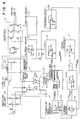
- Fig. 1 is a block diagram showing a power supply according to an embodiment of the present invention.
- 10 is a rectifier section
- 11 is a switching section
- 12 is a smoothing section
- 13 is an inverter
- 14 and 15 are current sensors
- 16 is a high-pass filter
- 17 is a phase inverter
- 18 is an automatic current regulator (ACR)
- 19 is a chopping and combining circuit
- 20 is a triangular wave generator circuit
- 21 is a driving circuit
- 22 is a control circuit.
- the current waveform of each section is also shown in Fig. 1.
- the a.c. supply voltage V s output from the a.c. power supply 1 is rectified in the rectifying section 10 and is sent to the switching section 11.
- the switching section 11 is composed of an inductor and switching elements (Tr1, Tr2, Tr3).
- Tr1, Tr2, Tr3 switching elements
- the switching element is controlled on and off.
- the part of the current output from the rectifying section 10 is flown to the smoothing capacitor through the inductor.
- the current sensor 15 serves to sense the current I c2 supplied to the smoothing section 12.
- the current I c2 contains lot of three or more degrees harmonics. From the current I c2 , only the harmonic components are extracted by the high-pass filter 16 having a higher cut-off frequency than the frequency of the a.c. supply voltage V s .
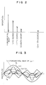
- Fig. 2 shows the effect of the high-pass filter 16.
- each mark " ⁇ " indicates the component of the input current I c2 of the high-pass filter 16 and each mark "X" indicates the component of the output current of the high-pass filter 16. That is to say, the output current of the high-pass filter 16 is a result of attenuating the fundamental component having the same frequency as the a.c. supply voltage from the current I c2 .
- I1 is the fundamental component of the current I c2
- 13 is a third or more degree harmonic component
- I4 is the output current of the high-pass filter 16.
- the output current I4 of the high-pass filter 16 is a result of combining all the harmonics.
- the phase of the output current I4 of the high-pass filter 16 is reversed by 180° at the phase reverser 17, and the resulting current I4 is supplied to the automatic current regulator 18 as a reference current (-I4).
- the current sensor 14 serves to sense the current I c1 to be chopped in the switching section 11 and supply the sensed current I c1 to the automatic current regulator 18.
- the chopping and combining circuit 19 serves to produce a pulse signal depending on a conduction ratio defined from a triangular wave signal output from the triangular wave generator circuit 20. Based on the pulse signal, the driving circuit 21 serves to control on and off the switching element included in the switching section 11.
- the automatic current regulator 18 serves to increase the conduction ratio of the switching elements T r1 , T r2 , T r3 , thereby keeping the load current sinusoidal.
- the switching section 11 serves as cancelling the harmonic components of the current I c2 , so that the a.c. load current I s is allowed to be constantly kept sinusoidal independently of the type and the magnitude of the load.
- the triangular wave generator circuit 20 serves to define the maximum switching frequency of the switching element included in the switching section 11. Unlike the prior arts, therefore, part of the switching frequency is not allowed to be abnormally higher. It results in reducing the switching loss of the switching element.
- the present embodiment has described that the current I c2 is sensed by winding a secondary coil around the inductor of the smoothing section.
- the use of a hole element sensor makes it possible to directly sense the waveform of the current.
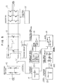
- Fig. 4 shows a power supply according to another embodiment of the present invention. This embodiment is analogous to the embodiment shown in Fig. 1 except provision of an averaging circuit 51.
- Fig. 1 consider that the current sensors 14 and 15 have respective amplification factors or accuracies. In this case, an error appears about the compared result between the current I c1 and the reference current (-I4) in the automatic current regulator 18. The appearance of the error results in having an adverse effect on the a.c. load current I s .
- the switching section 11 works to set a bit larger conduction ratio of the switching element, resulting in intensifying a three-degree harmonic, thereby distorting the waveform of the a.c. load current.
- the conduction ratio is set smaller, resulting in distorting the waveform of the a.c. load current as well.
- the current I c2 sensed by the current sensor 15 is averaged in the averaging circuit 51.
- the resulting averaged signal is used to control the amplification factor of the current sensor 14.
- the amplification factors of the current sensors 14 and 15 may be controlled (for example, to be equal to each other) so that the a.c. load current I s is made sinusoidal.
- Fig. 5 shows a power supply according to another embodiment of the present invention.
- the high-pass filter 16 and the phase reverser circuit 17 shown in Fig. 1 the averaging circuit 23 and the sinusoidal wave generator circuit 24 are used and the current sensor 14 is used for sensing the current I s ' output from the rectifying section 10.
- the averaging circuit 23 serves to sense an average value of the current I s ' sensed by the current sensor 14.
- the sinusoidal wave generator circuit 24 serves to generate a sinusoidal wave current having the same frequency as the a.c. supply voltage V s and the amplitude defined according to the averaged value and is sent as a reference current to the automatic current regulator 18.
- the automatic current regulator 18 serves to define such a conduction ratio for the switching element as matching the waveform of the current I s ' sensed by the current sensor 14 to that of the reference current.
- the conduction ratio is defined as monitoring the waveform of the current like the foregoing embodiments shown in Figs. 1 and 4.
- this embodiment has the same advantages as those foregoing embodiments.
- this embodiment may be arranged to control the current waveform with low-capacitance switching elements if it has a plurality of switching elements connected in parallel and controlled on and off in sequence.
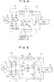
- Fig. 6 is a circuit diagram showing a power supply according to another embodiment of the present invention.
- 4 is a capacitor
- 25 is an inductor
- D15 to D19 are diodes
- T a and T b are transistors.
- the components corresponding to those shown in Fig. 1 have the same reference numbers.
- the rectifying section 10 is composed of the diodes D15 to D18 for performing the full wave rectification of the a.c. supply voltage V s .
- the switching section 11 is composed of an inductor 25 and two transistors T a and T b .
- the smoothing section 12 is composed of the diode D19 and the smoothing capacitor 4.
- the inductor 25, the diode D19, and the smoothing capacitor 4 are connected in series between two output terminals of the rectifying section 10.
- the series connection of the diode D19 and the smoothing capacitor 4 is connected to the two transistors T a and T b connected in parallel.
- the diode D19 is forward-biased and the transistors T a and T b are set off. It results in making the output voltage of the rectifying section 10 smoothed by the voltage charged in the smoothing capacitor 4 and applying the smoothed voltage as a d.c. supply voltage to the load 5.
- the voltage charged in the smoothing capacitor 4 depends on the magnitude of the load 5 and the constants of the inductor 25 and the smoothing capacitor 4. In general, however, the charged voltage is close to the a.c. supply voltage V s .
- the diode D19 is reverse-biased. Hence, if the transistors T a and T b are not operative, no a.c. load current I s flows and thus the a.c. load current I s has a waveform containing lots of three-degree harmonics, resulting in lowering a power factor of the a.c. power supply 1.
- the transistors T a and T b are controlled on and off in a manner that the transistors T a and T b are alternately switched on.
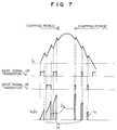
- the control circuit 101 serves to reduce the on-state period of the transistor T a or T b for reducing the switching loss.
- the inductor 25 works to emit the stored energy as a high voltage. It results in being able to flow current from the inductor 25 to the diode D19, the smoothing capacitor 4, the diode D17 or D18, the a.c. power supply 1, and the diode D15 or D16.
- This operation makes it possible to flow the a.c. load current I s when the output voltage of the rectifying section 10 is lower than the voltage charged in the smoothing capacitor 4.
- the transistors T a and T b are controlled on and off so that the a.c. load current I s can have a sinusoidal waveform.
- this embodiment is arranged to alternately control the two transistors T a and T b on and off.
- the amount of current flown through each of the two transistors T a and T b is made smaller than the amount of current flown through a single transistor. It results in reducing the on-state voltage loss and the switching loss of the transistors T a and T b . It means that small-capacitance transistors may be used for the transistors T a and T b .
- the number of the transistors used in the power supply is two, since those trnasistors have small capacitance, they can be accommodated as small-capacitance module components or a one-chip component in a single package. It results in reducing the overall power supply in size.
- the power supply according to this embodiment can be easily made from the conventional power supply in light of the circuit arrangement.
- Fig. 8 is a circuit diagram showing a power supply according to another embodiment of the present invention.
- 26 and 27 are inductors and D20 is a diode.
- the components corresponding to those shown in Figs. 1 and 13 have the same reference numbers.
- the present embodiment has the similar arrangement to the conventional power supply shown in Fig. 13 except that the current is supplied to the smoothing section through two current passages, that is, a current passage led from the rectifying section 10 and the other current passage composed of the inductor 27 and the diode D20 of the switching section 11.
- this embodiment is arranged to provide in a rectifying section 10 an inductor 26 between an output terminal of the rectifying section 10 and cathodes of diodes D1 and D2 and in a switching section 11 another inductor 27 between cathodes of diodes D5 and D6 and a collector of the transistor T.
- the collector of the transistor T is connected to the output terminal of the rectifying section 10.
- the transistor T is switched off, so that the a.c. supply voltage V s is full-wave rectified by the full wave rectifying circuit composed of the diodes D1 to D4 of the rectifying section 10 and is smoothed in the smoothing capacitor 4.
- the smoothed voltage is applied as a d.c. supply voltage to the load 5.
- the charging current I c2 is flown from the diode D1 or D2 to the smoothing capacitor 4 through the inductor 26.
- the inductor 26 serves to remove high-frequency components such as noise from the charging current I c2 .
- the absolute value of the a.c. supply voltage V s is low enough to make the output voltage of the full wave rectifier circuit composed of the diodes D1 to D4 lower than the votlage charged in the smoothing capacitor 4.
- the diodes D1 to D4 are reverse-biased, resulting in reducing the current I c2 flowing through the inductor 26 to zero.
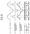
- the resulting current I c2 has a waveform containing lots of three-degree harmonics as shown in Fig. 9.
- the transistor T is controlled on and off for chopping the current I c1 output from the full wave rectifier circuit composed of the diodes D3 to D6 included in the rectifying section 10.
- the current I c1 is flown from the power supply 1 to the diode D5 or D6, the inductor 27, the transistor T, the diode D4 or D3.
- the inductor 27 stores the current I c1 as energy.
- the inductor 27 emits the stored energy as a high voltage. It results in being able to flow the current I c1 from the inductor 27 to the diode D20, the smoothing capacitor 4, the diode D4 or D3, the a.c. power supply 1 and the diode D5 or D6.
- Fig. 9 shows the waveform of the current I c1 supplied by the above-mentioned operation.
- the a.c. load current I s of the a.c. power supply 1 is a combined current of the currents I c1 and I c2 .
- the waveform of the a.c. load current I s is close to a sine wave as shown in Fig. 9.
- the embodiment shown in Fig. 8 is capable of reducing the on-state voltage loss and the switching loss of the transistor T as compared with the embodiment shown in Fig. 13, resulting in reducing the capacitance and the size of the transistor T.
- Fig. 11 is a circuit diagram showing a power supply according to another embodiment of the present invention.
- 25a and 25b are inductors
- D 19a and D 19b are diodes
- T a and T b are transistors.
- the components corresponding to those shown in the above-indicated drawings have the same reference numbers.
- the control circuit 101 serves to alternately control the transistors T a and T b on and off.
- the control circuit 101 contains two systems of normal chopper circuits. With the transistor T a being switched on, the current is flown from the full wave rectifier circuit to the inductor 25a and the transistor. The current is stored as energy in the inductor 25a. With the transistor T a being switched off, the inductor 25a emits the stored energy as a high voltage, resulting in being able to flow current from the inductor 25a to the diode D 19a , the smoothing capacitor 4, the diode D4 or D3, the a.c. power supply 1, and the diode D1 or D2.
- the inductor 25b stores energy. With the transistor T b being switched off, the inductor 25b emits the charged energy, resulting in being able to flow current from the inductor 25b to the diode D 19b and the above components.
- the a.c. power supply 1 is capable of supplying the a.c. load current I s having a waveform close to a sine wave.
- the power supply according to the present embodiment can lower the on-state voltage loss and the switching loss of the transistors T a and T b as compared to the power supply using a single transistor. It results in being able to reduce the capacitance and the size of the used transistors T a and T b .
- Fig. 12 is a circuit diagram showing a power supply according to an embodiment of the present invention.
- 28a and 28b are inductors
- D 21a , D 21b , D 22a and D 22b are diodes
- T a and T b are transistors.
- the components corresponding to those shown in Fig. 16 have the same reference numbers.
- the present embodiment has the same arrangement as the conventional power supply using the voltage doubler rectifier circuit shown in Fig. 16, except that the inductors 28a, 28b, the diodes D 21a , D 21b , D 22a , D 22b , and the transistors T a , T b are provided in place of the diodes D12, D14 and the transsitors T A and T B shown in Fig. 16.
- two series circuits are provided in parallel to the a.c. power supply 1, one series circuit being composed of the inductor 28a, the diode D 22a and the npn type transistor T a and the other series circuit being composed of the inductor 28b, the diode D 22b and the pnp type transistor T b .
- the diode D 21a is connected between an anode of the diode D 22a and a cathode of the diode D11 and the diode D 21b is connected between a cathode of the diode D 22b and an anode of the diode D13.
- this embodiment operates in the same manner as the conventional power supply shown in Fig. 16.
- the smoothing capacitor 4A is charged during that period while keeping the a.c. supply voltage V s at the positive polarity indicated by an arrow.
- the smoothing capacitor 4B is charged during that period while keeping the a.c. supply voltage V s at a negative polarity opposite to the polarity indicated by the arrow.
- the transistors T a and T b are switched off.
- the transistors T a and T b are controlled on and off by the control circuit 101 having two systems of normal chopper circuits.
- the transistor T a With the transistor T a being switched on, the current flows through the inductor 28a, the diode D 22a and the transistor T a , resulting in storing energy in the inductor 28a. Then, with the transistor T a being switched off, the inductor 28a serves to emit the stored energy as a high voltage, resulting in being able to flow current through the inductor 28a, the diode D 21a , the smoothing capacitor 4A, and the a.c. power supply 1. With the transistor T b being switched on, the current flows through the transistor T b , the diode D 22b and the inductor 28b, resulting in storing energy in the inductor 28b.
- the inductor 29b serves to emit the stored energy as a high voltage, resulting in being able to flow current through the inductor 28b, the a.c. power supply 1, the smoothing capacitor 4B and the diode D 21b .
- this embodiment makes it possible to produce the a.c. load current I s having a waveform closing to a sine wave.
- the transistors T a and T b are controlled on and off if the a.c. supply voltage V s is a relatively high, part of the a.c. load current is allowed to flow through the transistors T a and T b .
- this embodiment is capable of reducing the on-state voltage loss and the switching loss of the transistors T a and T b as compared with the conventional power supply shown in Fig. 16 and using as the transistors T a and T b small transistors with low capacitance.
Landscapes
- Engineering & Computer Science (AREA)
- Power Engineering (AREA)
- Physics & Mathematics (AREA)
- Electromagnetism (AREA)
- General Physics & Mathematics (AREA)
- Radar, Positioning & Navigation (AREA)
- Automation & Control Theory (AREA)
- Rectifiers (AREA)
- Control Of Electrical Variables (AREA)
- Ac-Ac Conversion (AREA)
- Inverter Devices (AREA)
Applications Claiming Priority (2)
| Application Number | Priority Date | Filing Date | Title |
|---|---|---|---|
| JP2315935A JPH04188206A (ja) | 1990-11-22 | 1990-11-22 | 電源装置 |
| JP315935/90 | 1990-11-22 |
Publications (3)
| Publication Number | Publication Date |
|---|---|
| EP0486875A2 true EP0486875A2 (de) | 1992-05-27 |
| EP0486875A3 EP0486875A3 (en) | 1992-12-02 |
| EP0486875B1 EP0486875B1 (de) | 1996-02-07 |
Family
ID=18071374
Family Applications (1)
| Application Number | Title | Priority Date | Filing Date |
|---|---|---|---|
| EP91118911A Expired - Lifetime EP0486875B1 (de) | 1990-11-22 | 1991-11-06 | Leistungsversorgung gesteuert für einen sinusförmigen Laststrom |
Country Status (6)
| Country | Link |
|---|---|
| US (1) | US5245522A (de) |
| EP (1) | EP0486875B1 (de) |
| JP (1) | JPH04188206A (de) |
| KR (1) | KR950010130B1 (de) |
| DE (1) | DE69116995T2 (de) |
| ES (1) | ES2082907T3 (de) |
Cited By (5)
| Publication number | Priority date | Publication date | Assignee | Title |
|---|---|---|---|---|
| EP0586885A1 (de) * | 1992-08-06 | 1994-03-16 | Mitsubishi Denki Kabushiki Kaisha | Vorrichtung für Gleichstrom-Leistungsversorgung |
| FR2738689A1 (fr) * | 1995-08-16 | 1997-03-14 | Telefunken Microelectron | Procede pour reduire la creation d'harmoniques dans le reseau d'alimentation par la commande de machines electriques |
| EP0820136A3 (de) * | 1996-07-16 | 1998-06-10 | Hitachi, Ltd. | Stromversorgungseinrichtung für eine Klima-Anlage |
| EP0786857A4 (de) * | 1995-07-11 | 1999-12-29 | Meidensha Electric Mfg Co Ltd | Wandlerschaltkreis mit sinusförmiger stromaufnahme |
| FR2937808A1 (fr) * | 2008-10-29 | 2010-04-30 | Converteam Technology Ltd | Systeme de conversion d'un courant electrique alternatif d'entree en un courant electrique continu de sortie, a correction de facteur de puissance, et equipement electrique de puissance comportant un tel systeme de conversion |
Families Citing this family (26)
| Publication number | Priority date | Publication date | Assignee | Title |
|---|---|---|---|---|
| JP3363170B2 (ja) * | 1992-02-10 | 2003-01-08 | 本田技研工業株式会社 | インバータ制御式発電機 |
| WO1993026078A1 (en) * | 1992-06-10 | 1993-12-23 | Digital Equipment Corporation | High power factor switched dc power supply |
| US5371667A (en) * | 1993-06-14 | 1994-12-06 | Fuji Electrochemical Co., Ltd. | Electric power supply |
| US5610805A (en) * | 1995-01-10 | 1997-03-11 | Cambridge Continuous Power | Uninterruptible power supply with a back-up battery coupled across the a.c. input |
| JP2818641B2 (ja) * | 1995-01-26 | 1998-10-30 | 富士電気化学株式会社 | スイッチング電源 |
| US5568041A (en) * | 1995-02-09 | 1996-10-22 | Magnetek, Inc. | Low-cost power factor correction circuit and method for electronic ballasts |
| US5650705A (en) * | 1995-02-13 | 1997-07-22 | Hart; John Roger | Apparatus and method for controlling currents in an inductor |
| JP3412329B2 (ja) * | 1995-04-24 | 2003-06-03 | 株式会社デンソー | 車両用発電装置 |
| US5745499A (en) * | 1995-10-11 | 1998-04-28 | Micron Technology, Inc. | Supervoltage detection circuit having a multi-level reference voltage |
| DE19729705A1 (de) * | 1997-07-11 | 1999-01-14 | Philips Patentverwaltung | Schaltungsanordnung zum Speisen einer Last |
| US6166929A (en) * | 2000-02-29 | 2000-12-26 | Rockwell Technologies, Llc | CSI based drive having active damping control |
| JP3890184B2 (ja) * | 2000-05-15 | 2007-03-07 | Necパーソナルプロダクツ株式会社 | 電源装置及びその電力制御方法、情報処理機器 |
| US7663898B2 (en) * | 2004-06-07 | 2010-02-16 | Ixys Corporation | Switching power supply with direct conversion off AC power source |
| JP2006087235A (ja) * | 2004-09-16 | 2006-03-30 | Sanken Electric Co Ltd | 力率改善回路及び力率改善回路の制御回路 |
| KR101026248B1 (ko) * | 2004-09-21 | 2011-03-31 | 페어차일드코리아반도체 주식회사 | 역률 보상 회로 |
| US7927948B2 (en) | 2005-07-20 | 2011-04-19 | Micron Technology, Inc. | Devices with nanocrystals and methods of formation |
| US7382112B2 (en) * | 2005-08-16 | 2008-06-03 | The Board Of Trustees Of The University Of Illinois | Methods and devices for input waveform control in switching power supplies |
| DE102006029389A1 (de) * | 2006-06-27 | 2008-01-10 | Robert Bosch Gmbh | Verfahren zur Erweiterung der Diagnosefähigkeit von Stromreglern |
| JP4067021B2 (ja) * | 2006-07-24 | 2008-03-26 | ダイキン工業株式会社 | インバータ装置 |
| JP2010131624A (ja) * | 2008-12-04 | 2010-06-17 | Toyo Electric Mfg Co Ltd | 間欠負荷駆動用電動機制御装置。 |
| JP5464851B2 (ja) * | 2008-12-16 | 2014-04-09 | 三菱電機株式会社 | インバータ装置 |
| CN101656482B (zh) * | 2009-09-04 | 2012-09-05 | 上海交通大学 | 三相整流上电装置 |
| US8351232B2 (en) * | 2009-12-28 | 2013-01-08 | Nxp B.V. | Power factor corrector with high power factor at low load or high mains voltage conditions |
| US9099934B2 (en) * | 2012-01-10 | 2015-08-04 | Yaskawa America, Inc. | Three phase active rectifier system |
| CN104620483B (zh) * | 2012-05-31 | 2017-05-31 | 松下电器产业株式会社 | 电力转换电路的控制装置 |
| CN104380586B (zh) * | 2013-06-04 | 2017-12-12 | 东芝三菱电机产业系统株式会社 | 功率转换装置 |
Family Cites Families (7)
| Publication number | Priority date | Publication date | Assignee | Title |
|---|---|---|---|---|
| US4467268A (en) * | 1980-04-30 | 1984-08-21 | Raytheon Company | Digitally controlled power supply |
| JPS573579A (en) * | 1980-06-09 | 1982-01-09 | Hitachi Ltd | Electric-power supply device |
| JPS5914021A (ja) * | 1982-07-15 | 1984-01-24 | Matsushita Electric Works Ltd | 整流電源回路 |
| JPS61224857A (ja) * | 1985-03-29 | 1986-10-06 | Hitachi Ltd | 整流回路の制御装置 |
| JPS6245794A (ja) * | 1985-08-26 | 1987-02-27 | ハイモ株式会社 | 紙力増強方法 |
| JPH0695884B2 (ja) * | 1986-07-14 | 1994-11-30 | 旭電化工業株式会社 | 高粘性フイリングの製造方法 |
| CA1295014C (en) * | 1986-08-01 | 1992-01-28 | Christopher Paul Henze | Digitally controlled a.c. to d.c. power conditioner that draws sinusoidal input current |
-
1990
- 1990-11-22 JP JP2315935A patent/JPH04188206A/ja active Pending
-
1991
- 1991-11-06 ES ES91118911T patent/ES2082907T3/es not_active Expired - Lifetime
- 1991-11-06 DE DE69116995T patent/DE69116995T2/de not_active Expired - Fee Related
- 1991-11-06 EP EP91118911A patent/EP0486875B1/de not_active Expired - Lifetime
- 1991-11-15 US US07/792,405 patent/US5245522A/en not_active Expired - Fee Related
- 1991-11-19 KR KR1019910020537A patent/KR950010130B1/ko not_active Expired - Fee Related
Cited By (8)
| Publication number | Priority date | Publication date | Assignee | Title |
|---|---|---|---|---|
| EP0586885A1 (de) * | 1992-08-06 | 1994-03-16 | Mitsubishi Denki Kabushiki Kaisha | Vorrichtung für Gleichstrom-Leistungsversorgung |
| US5479336A (en) * | 1992-08-06 | 1995-12-26 | Mitsubishi Denki Kabushiki Kaisha | DC power-supply unit |
| AU666027B2 (en) * | 1992-08-06 | 1996-01-25 | Mitsubishi Denki Kabushiki Kaisha | DC power-supply unit |
| EP0786857A4 (de) * | 1995-07-11 | 1999-12-29 | Meidensha Electric Mfg Co Ltd | Wandlerschaltkreis mit sinusförmiger stromaufnahme |
| FR2738689A1 (fr) * | 1995-08-16 | 1997-03-14 | Telefunken Microelectron | Procede pour reduire la creation d'harmoniques dans le reseau d'alimentation par la commande de machines electriques |
| EP0820136A3 (de) * | 1996-07-16 | 1998-06-10 | Hitachi, Ltd. | Stromversorgungseinrichtung für eine Klima-Anlage |
| US5929591A (en) * | 1996-07-16 | 1999-07-27 | Hitachi, Ltd. | Air conditioner |
| FR2937808A1 (fr) * | 2008-10-29 | 2010-04-30 | Converteam Technology Ltd | Systeme de conversion d'un courant electrique alternatif d'entree en un courant electrique continu de sortie, a correction de facteur de puissance, et equipement electrique de puissance comportant un tel systeme de conversion |
Also Published As
| Publication number | Publication date |
|---|---|
| JPH04188206A (ja) | 1992-07-06 |
| KR920010391A (ko) | 1992-06-26 |
| DE69116995T2 (de) | 1996-09-26 |
| EP0486875A3 (en) | 1992-12-02 |
| DE69116995D1 (de) | 1996-03-21 |
| EP0486875B1 (de) | 1996-02-07 |
| KR950010130B1 (ko) | 1995-09-07 |
| US5245522A (en) | 1993-09-14 |
| ES2082907T3 (es) | 1996-04-01 |
Similar Documents
| Publication | Publication Date | Title |
|---|---|---|
| EP0486875B1 (de) | Leistungsversorgung gesteuert für einen sinusförmigen Laststrom | |
| KR0152252B1 (ko) | 5핀을 갖는 능동역률보정집적회로 | |
| US6690586B2 (en) | Switching power source device | |
| US11005356B2 (en) | Power supply control device and LLC resonant converter | |
| US7208883B2 (en) | Current detection circuit, and power supply apparatus, power supply system and electronic apparatus using the current detection circuit | |
| JPH06335241A (ja) | トランス結合型2次直流電源生成装置 | |
| US4163278A (en) | Voltage supply circuit responsive to plural possible DC input levels | |
| EP0690553A2 (de) | Stormversorgungseinheit | |
| EP0726640A2 (de) | Gleichrichter-Leistungsversorgungsschaltung | |
| GB2188498A (en) | Self oscillating dc-ac-dc converter | |
| US5625538A (en) | High power factor power-supply system | |
| EP0259889B1 (de) | Geregeltes Schaltnetzteil | |
| US7443699B2 (en) | Negative current compensation method and circuit | |
| EP0061730A2 (de) | Transistor-Wechselrichtereinrichtung | |
| JP3252540B2 (ja) | インバータ装置 | |
| JPH02168855A (ja) | スイッチング電源装置 | |
| JPS6151510B2 (de) | ||
| JP2554736Y2 (ja) | スイッチングレギュレ−タ | |
| KR19980028177A (ko) | 고역률 보상회로 | |
| JPH11225474A (ja) | Dc−dcコンバータ | |
| KR0162382B1 (ko) | 하프 브릿지 인버터의 전력 제어회로 | |
| KR950002931B1 (ko) | 전원장치 | |
| JPS627370A (ja) | 直流変換器 | |
| JP2000032754A (ja) | 多出力スイッチングレギュレータ及びその出力制御方法 | |
| JPS6364149B2 (de) |
Legal Events
| Date | Code | Title | Description |
|---|---|---|---|
| PUAI | Public reference made under article 153(3) epc to a published international application that has entered the european phase |
Free format text: ORIGINAL CODE: 0009012 |
|
| 17P | Request for examination filed |
Effective date: 19911106 |
|
| AK | Designated contracting states |
Kind code of ref document: A2 Designated state(s): DE ES FR SE |
|
| PUAL | Search report despatched |
Free format text: ORIGINAL CODE: 0009013 |
|
| AK | Designated contracting states |
Kind code of ref document: A3 Designated state(s): DE ES FR SE |
|
| 17Q | First examination report despatched |
Effective date: 19940422 |
|
| GRAA | (expected) grant |
Free format text: ORIGINAL CODE: 0009210 |
|
| AK | Designated contracting states |
Kind code of ref document: B1 Designated state(s): DE ES FR SE |
|
| REF | Corresponds to: |
Ref document number: 69116995 Country of ref document: DE Date of ref document: 19960321 |
|
| REG | Reference to a national code |
Ref country code: ES Ref legal event code: FG2A Ref document number: 2082907 Country of ref document: ES Kind code of ref document: T3 |
|
| ET | Fr: translation filed | ||
| PLBE | No opposition filed within time limit |
Free format text: ORIGINAL CODE: 0009261 |
|
| STAA | Information on the status of an ep patent application or granted ep patent |
Free format text: STATUS: NO OPPOSITION FILED WITHIN TIME LIMIT |
|
| 26N | No opposition filed | ||
| PGFP | Annual fee paid to national office [announced via postgrant information from national office to epo] |
Ref country code: SE Payment date: 20020923 Year of fee payment: 12 |
|
| PGFP | Annual fee paid to national office [announced via postgrant information from national office to epo] |
Ref country code: FR Payment date: 20021023 Year of fee payment: 12 |
|
| PGFP | Annual fee paid to national office [announced via postgrant information from national office to epo] |
Ref country code: ES Payment date: 20021105 Year of fee payment: 12 |
|
| PGFP | Annual fee paid to national office [announced via postgrant information from national office to epo] |
Ref country code: DE Payment date: 20021205 Year of fee payment: 12 |
|
| PG25 | Lapsed in a contracting state [announced via postgrant information from national office to epo] |
Ref country code: SE Free format text: LAPSE BECAUSE OF NON-PAYMENT OF DUE FEES Effective date: 20031107 Ref country code: ES Free format text: LAPSE BECAUSE OF NON-PAYMENT OF DUE FEES Effective date: 20031107 |
|
| PG25 | Lapsed in a contracting state [announced via postgrant information from national office to epo] |
Ref country code: DE Free format text: LAPSE BECAUSE OF NON-PAYMENT OF DUE FEES Effective date: 20040602 |
|
| EUG | Se: european patent has lapsed | ||
| PG25 | Lapsed in a contracting state [announced via postgrant information from national office to epo] |
Ref country code: FR Free format text: LAPSE BECAUSE OF NON-PAYMENT OF DUE FEES Effective date: 20040730 |
|
| REG | Reference to a national code |
Ref country code: FR Ref legal event code: ST |
|
| REG | Reference to a national code |
Ref country code: ES Ref legal event code: FD2A Effective date: 20031107 |