EP0487064A2 - Circuit pour générer des adresses et dispositif CD-ROM utilisant un tel circuit - Google Patents
Circuit pour générer des adresses et dispositif CD-ROM utilisant un tel circuit Download PDFInfo
- Publication number
- EP0487064A2 EP0487064A2 EP91119784A EP91119784A EP0487064A2 EP 0487064 A2 EP0487064 A2 EP 0487064A2 EP 91119784 A EP91119784 A EP 91119784A EP 91119784 A EP91119784 A EP 91119784A EP 0487064 A2 EP0487064 A2 EP 0487064A2
- Authority
- EP
- European Patent Office
- Prior art keywords
- rom
- ram
- line
- column
- addresses
- Prior art date
- Legal status (The legal status is an assumption and is not a legal conclusion. Google has not performed a legal analysis and makes no representation as to the accuracy of the status listed.)
- Granted
Links
Images


Classifications
-
- G—PHYSICS
- G06—COMPUTING OR CALCULATING; COUNTING
- G06F—ELECTRIC DIGITAL DATA PROCESSING
- G06F11/00—Error detection; Error correction; Monitoring
- G06F11/07—Responding to the occurrence of a fault, e.g. fault tolerance
- G06F11/08—Error detection or correction by redundancy in data representation, e.g. by using checking codes
- G06F11/10—Adding special bits or symbols to the coded information, e.g. parity check, casting out 9's or 11's
- G06F11/1008—Adding special bits or symbols to the coded information, e.g. parity check, casting out 9's or 11's in individual solid state devices
-
- G—PHYSICS
- G11—INFORMATION STORAGE
- G11B—INFORMATION STORAGE BASED ON RELATIVE MOVEMENT BETWEEN RECORD CARRIER AND TRANSDUCER
- G11B20/00—Signal processing not specific to the method of recording or reproducing; Circuits therefor
- G11B20/10—Digital recording or reproducing
- G11B20/18—Error detection or correction; Testing, e.g. of drop-outs
- G11B20/1833—Error detection or correction; Testing, e.g. of drop-outs by adding special lists or symbols to the coded information
Definitions
- This invention relates to an address generating circuit and a compact disk random access memory (CD-ROM) device using the same, and more particularly to, an address generating circuit which generates an address of a memory in case of error correction and a CD-ROM device using the same.
- CD-ROM compact disk random access memory
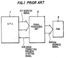
- a conventional CD-ROM device includes a central processing unit (CPU), a signal processing unit and a random access memory (RAM).
- CPU central processing unit
- RAM random access memory
- the signal processing unit supplies the CPU with an error correction process starting signal.
- the CPU supplies the signal processing unit with an address signal calculated in accordance with the error correction process starting signal.
- the signal processing unit supplies the RAM with the calculated address signal as a RAM address signal, at which stored data are corrected in the RAM.
- an address generating circuit comprises: a line counter for counting a line number of addresses of a RAM; a column counter for counting a column number of addresses of the RAM; a first logic circuit for making a sum of outputs of the line and column counters; a modulator for modulating an output of the logic circuit; a first selector for selecting an output from outputs of the line and column counters and the modulator; a ROM in which start addresses of the lines of addresses are stored; a second selector for selecting an output from outputs of the line and column counters; and a second logic circuit for making a sum of outputs of the ROM and the second selector to be supplied to the RAM as an address.
- a CD-ROM device comprises; a RAM for storing data to be read from a CD-ROM; a CPU for controlling operation of reading data from the CD-ROM; and a signal processing unit for processing signals between the RAM and the CPU, the signal processing unit comprising an address generating circuit which comprises a line counter for counting a line number of addresses of a RAM, a column counter for counting a column number of addresses of the RAM, a first logic circuit for making a sum of outputs of the line and column counters, a modulator for modulating an output of the logic circuit, a first selector for selecting an output from outputs of the line and column counters and the modulator, a ROM in which start addresses of the lines of addresses are stored, a second selector for selecting an output from outputs of the line and column counters, and a second logic circuit for making a sum of outputs of the ROM and the second selector to be supplied to the RAM as an address.
- an address generating circuit which comprises a line counter for counting a line number of addresses of a
- a conventional CD-ROM device includes a CPU 7, a signal processing unit 8 and a RAM 9.
- the RAM 9 is stored with data read from a CD-ROM device (not shown).
- the stored data is processed in the signal processing unit 8.
- error data may be stored in the RAM 9.
- an address of the data correction must be generated in the address signal generating cirucit.
- the RAM address signal is supplied from the signal processing unit 8 as a result of logic calculation process by the CPU 7, as explained before, so that the provability of error data correction is relatively small, and the CPU 7 is burdened with heavy load including such address generation.
- FIG. 2 shows an address generating circuit in a preferred embodiment.
- the address generating circuit includes a line counter 1 which counts line numbers of addresses, a column counter 2 which counts column numbers thereof, a first arithmetic logic unit 3 which makes a sum of outputs of the line and column counters 1 and 2, a modulator 4 which modulates an output of the first arithmetic logic unit 3, a first selector 11 which selects an output from outputs of the line and column counters 1 and 2 and the modulator 4 in accordance with P- and Q-system selecting signals 101 and 102 and a Q-parity selecting signal 103, a ROM 5 which stores start addresses of the address lines and supplies an output in accordance with an output of the first selector 11, a second selector 12 which selects an output from outputs of the line and column counters 1 and 2 and the ROM 5 in accordance with a Q-parity selecting signal 104 and a system selecting signal 105, and
- the ROM 5 stores the start address "0000", “0043”, “0066”, .... of the line addresses at the counted number of "0" of the column counter 1, as described in an address map of the RAM 8 shown in Fig. 3, in which Q- and P-systems of address generation are indicated by arrows.
- the first arithmetic logic unit 3 makes a sum of contents of the line and column counters 1 and 2.
- the modulator 4 generates a modulated number from an output of the first arithmetic logic unit 3. When the input becomes "26”, then the modulator 4 supplies "0", and increases the number again.
- the column number of the column counter 2 becomes "43” or "44”, those numbers are identified as Q-parities, so that the predetermined addresses of "1118" or "1144" are designated in the ROM 5. Then, the column number of the column counter 2 is set to be "0".
- the first selector 11 selects the output of the modulator 4 in accordance with the Q-system selecting signal 101 to be supplied to the ROM 5 when the column number of the address column is at most "42".
- the ROM 5 supplies the start address of the address lines to be supplied to the second arithmetic logic unit 6.
- the second selector 12 selects an output of the column counter 2 in accordance with the system selecting signal 105 to be supplied to the second arithmetic logic unit 6.
- the second arithmetic logic unit 6 makes a sum of the start address read from the ROM 5 and the counted number of the column counter 2 to be supplied to the RAM 9 as the RAM address signal 106.
- the first selector 11 selects the output of the column counter 2 to be supplied to the ROM 5 in accordance with the Q-parity selecting signal 103, so that the ROM 5 supplies the addresses of "1118” or "1144" to the second arithmetic logic, unit 6, respectively.
- the second selector 12 selects the output of the line counter 1 to be supplied to the second arithmetic logic unit 6 in accordance with the Q-parity selecting signal 104.
- the second arithmetic logic unit 6 makes a sum of the predetermined address of "1118” or "1144" and the counted number of the line counter 1 to be supplied to the RAM 9 as the RAM address signal 106.
- the first selector 11 selects the output of the line counter 1 in accordance with the P-system selecting signal 101 to be supplied to the ROM 5 when the column number of the address column is at most "42".
- the ROM 5 supplies the start address of the address lines to be supplied to the second arithmetic logic unit 6.
- the second selector 12 selects an output of the column counter 2 in accordance with the system selecting signal 105 to be supplied to the second arithmetic logic unit 6.
- the second arithmetic logic unit 6 makes a sum of the start address road from the ROM 5 and the counted number of the column counter 2 to be supplied to the RAM 9 as the RAM address signal 106.
- the first selector 11 selects the output of the column counter 2 to be supplied to the ROM 5 in accordance with the Q-parity selecting signal 103, so that the ROM 5 supplies the addresses of "1118” or "1144" to the second arithmetic logic unit 6, respectively.
- the second selector 12 selects the output of the line counter 1 to be supplied to the second arithmetic logic unit 6 in accordance with the Q-parity selecting signal 104.
- the second arithmetic logic unit 6 makes a sum of the predetermined address of "1118” or "1144" and the line number of the address line to be supplied to the RAM 9 as the RAM address signal 106.
- the signal processing unit 8 includes the address generating circuit as explained above, so that the RAM address signal 106 is directly supplied to the RAM 9 from the signal processing unit 8 without using the CPU. Therefore, there requires fewer steps to generate addresses than those required in the conventional CD-ROM device, so that the provability of the error correction increases. Further, the load of the CPU is reduced, so that the CPU can exhibit its performance properly.
Landscapes
- Engineering & Computer Science (AREA)
- Theoretical Computer Science (AREA)
- Quality & Reliability (AREA)
- Physics & Mathematics (AREA)
- General Engineering & Computer Science (AREA)
- General Physics & Mathematics (AREA)
- Signal Processing (AREA)
- Error Detection And Correction (AREA)
- Signal Processing For Digital Recording And Reproducing (AREA)
Applications Claiming Priority (2)
| Application Number | Priority Date | Filing Date | Title |
|---|---|---|---|
| JP314731/90 | 1990-11-19 | ||
| JP2314731A JP2781658B2 (ja) | 1990-11-19 | 1990-11-19 | アドレス生成回路とそれを用いたcd―rom装置 |
Publications (3)
| Publication Number | Publication Date |
|---|---|
| EP0487064A2 true EP0487064A2 (fr) | 1992-05-27 |
| EP0487064A3 EP0487064A3 (en) | 1992-09-23 |
| EP0487064B1 EP0487064B1 (fr) | 1997-02-05 |
Family
ID=18056897
Family Applications (1)
| Application Number | Title | Priority Date | Filing Date |
|---|---|---|---|
| EP91119784A Expired - Lifetime EP0487064B1 (fr) | 1990-11-19 | 1991-11-19 | Circuit pour générer des adresses et dispositif CD-ROM utilisant un tel circuit |
Country Status (4)
| Country | Link |
|---|---|
| US (1) | US5524229A (fr) |
| EP (1) | EP0487064B1 (fr) |
| JP (1) | JP2781658B2 (fr) |
| DE (1) | DE69124574T2 (fr) |
Cited By (1)
| Publication number | Priority date | Publication date | Assignee | Title |
|---|---|---|---|---|
| EP0626646A1 (fr) * | 1993-05-25 | 1994-11-30 | Fujitsu Limited | Procédé de gestion de fichiers de données des supports de données interchangeables |
Families Citing this family (1)
| Publication number | Priority date | Publication date | Assignee | Title |
|---|---|---|---|---|
| EP1795992B1 (fr) * | 2002-07-30 | 2018-01-24 | Fujitsu Limited | Procédé et appareil de reproduction d'informations utilisant module de sécurité |
Family Cites Families (13)
| Publication number | Priority date | Publication date | Assignee | Title |
|---|---|---|---|---|
| JPS5279628A (en) * | 1975-12-25 | 1977-07-04 | Casio Comput Co Ltd | Information reading processing equipment |
| JPH07101543B2 (ja) * | 1984-03-24 | 1995-11-01 | ソニー株式会社 | エラー訂正符号化方法 |
| EP0156440B1 (fr) * | 1984-03-24 | 1990-01-24 | Koninklijke Philips Electronics N.V. | Méthode de transmission d'information avec correction d'erreurs des mots de données, méthode de décodage de correction d'erreurs pour les mots de données, un appareil de transmission d'information utilisant cette méthode, un appareil pour décoder l'information utilisant cette méthode et un dispositif utilisant un tel appareil |
| JPS60213132A (ja) * | 1984-04-06 | 1985-10-25 | Nec Corp | デイジタル信号処理装置 |
| JP2557340B2 (ja) * | 1984-10-31 | 1996-11-27 | 株式会社東芝 | デジタル再生装置におけるデインタ−リ−ブ処理用メモリの制御方法 |
| JPH0640420B2 (ja) * | 1985-02-27 | 1994-05-25 | 株式会社日立製作所 | Pcm再生装置 |
| GB2184268B (en) * | 1985-12-13 | 1989-11-22 | Anamartic Ltd | Fault tolerant memory system |
| JPS6359221A (ja) * | 1986-08-29 | 1988-03-15 | Nec Home Electronics Ltd | デインタリ−ブ回路 |
| JPS63181169A (ja) * | 1987-01-21 | 1988-07-26 | Matsushita Electric Ind Co Ltd | インタ−リ−ブデインタ−リ−ブ装置 |
| JP2713902B2 (ja) * | 1987-04-28 | 1998-02-16 | 三洋電機株式会社 | アドレス発生回路 |
| JP2829963B2 (ja) * | 1988-05-16 | 1998-12-02 | ソニー株式会社 | ディジタルデータ記録/再生装置 |
| US5257271A (en) * | 1989-07-29 | 1993-10-26 | Sony Corporation | Sample data transmission apparatus |
| KR930000994B1 (ko) * | 1990-08-09 | 1993-02-12 | 삼성전자 주식회사 | Cd-rom 데이타 버퍼링 및 독출용 어드레스 발생방법 및 회로 |
-
1990
- 1990-11-19 JP JP2314731A patent/JP2781658B2/ja not_active Expired - Lifetime
-
1991
- 1991-11-19 EP EP91119784A patent/EP0487064B1/fr not_active Expired - Lifetime
- 1991-11-19 DE DE69124574T patent/DE69124574T2/de not_active Expired - Fee Related
-
1995
- 1995-03-30 US US08/414,044 patent/US5524229A/en not_active Expired - Fee Related
Cited By (2)
| Publication number | Priority date | Publication date | Assignee | Title |
|---|---|---|---|---|
| EP0626646A1 (fr) * | 1993-05-25 | 1994-11-30 | Fujitsu Limited | Procédé de gestion de fichiers de données des supports de données interchangeables |
| US6189014B1 (en) * | 1993-05-25 | 2001-02-13 | Fujitsu Limited | File management method for interchangeable storage media |
Also Published As
| Publication number | Publication date |
|---|---|
| US5524229A (en) | 1996-06-04 |
| JP2781658B2 (ja) | 1998-07-30 |
| EP0487064B1 (fr) | 1997-02-05 |
| DE69124574D1 (de) | 1997-03-20 |
| DE69124574T2 (de) | 1997-09-04 |
| JPH04184769A (ja) | 1992-07-01 |
| EP0487064A3 (en) | 1992-09-23 |
Similar Documents
| Publication | Publication Date | Title |
|---|---|---|
| JPS5854472A (ja) | 画像処理装置及び方法 | |
| EP0330275A2 (fr) | Dispositif de décodage de télétext | |
| EP0487064A2 (fr) | Circuit pour générer des adresses et dispositif CD-ROM utilisant un tel circuit | |
| EP0114390B1 (fr) | Circuit pour la vérification d'une configuration de bits | |
| KR920000417B1 (ko) | 연산처리장치 | |
| US7162558B2 (en) | Interrupt signal processing circuit for sending interrupt requests to a computer system | |
| US5426766A (en) | Microprocessor which holds selected data for continuous operation | |
| EP0398654A2 (fr) | Appareil pour écrire des données dans une eeprom | |
| US6003110A (en) | Method and apparatus for converting memory addresses into memory selection signals | |
| US5428801A (en) | Data array conversion control system for controlling conversion of data arrays being transferred between two processing systems | |
| US5493727A (en) | Electronic equipment including means for controlling reading of control programs | |
| US4506340A (en) | Method and apparatus for producing the residue of the product of two residues | |
| JPS58197557A (ja) | メツセ−ジ管理方式 | |
| JP3190861B2 (ja) | 疑似nキーロールオーバキーボード入力装置と処理方法 | |
| KR910009296B1 (ko) | 순차접근 기억장치 | |
| JP2571090B2 (ja) | アドレス送信装置及び受信装置 | |
| KR0168973B1 (ko) | 어드레스를 자동 증가시켜 롬을 억세스하는 방법 및 그장치 | |
| JPS6020779B2 (ja) | 複合形電子計算機システム | |
| JPS61156491A (ja) | Icカ−ド | |
| JPS61143835A (ja) | デ−タ表示方式 | |
| JP2777128B2 (ja) | 保護継電器の整定回路 | |
| JPS61144019A (ja) | 電子ビーム露光装置のパターン・データ転送方法 | |
| JPH0314038A (ja) | 状態遷移表変換装置 | |
| JPH04137135A (ja) | プログラムメモリ制御回路 | |
| JPS6180447A (ja) | 記憶装置のストア制御方式 |
Legal Events
| Date | Code | Title | Description |
|---|---|---|---|
| PUAI | Public reference made under article 153(3) epc to a published international application that has entered the european phase |
Free format text: ORIGINAL CODE: 0009012 |
|
| AK | Designated contracting states |
Kind code of ref document: A2 Designated state(s): DE FR GB |
|
| 17P | Request for examination filed |
Effective date: 19920515 |
|
| PUAL | Search report despatched |
Free format text: ORIGINAL CODE: 0009013 |
|
| AK | Designated contracting states |
Kind code of ref document: A3 Designated state(s): DE FR GB |
|
| 17Q | First examination report despatched |
Effective date: 19940802 |
|
| GRAG | Despatch of communication of intention to grant |
Free format text: ORIGINAL CODE: EPIDOS AGRA |
|
| GRAH | Despatch of communication of intention to grant a patent |
Free format text: ORIGINAL CODE: EPIDOS IGRA |
|
| GRAH | Despatch of communication of intention to grant a patent |
Free format text: ORIGINAL CODE: EPIDOS IGRA |
|
| GRAA | (expected) grant |
Free format text: ORIGINAL CODE: 0009210 |
|
| AK | Designated contracting states |
Kind code of ref document: B1 Designated state(s): DE FR GB |
|
| REF | Corresponds to: |
Ref document number: 69124574 Country of ref document: DE Date of ref document: 19970320 |
|
| ET | Fr: translation filed | ||
| PLBE | No opposition filed within time limit |
Free format text: ORIGINAL CODE: 0009261 |
|
| STAA | Information on the status of an ep patent application or granted ep patent |
Free format text: STATUS: NO OPPOSITION FILED WITHIN TIME LIMIT |
|
| 26N | No opposition filed | ||
| REG | Reference to a national code |
Ref country code: GB Ref legal event code: IF02 |
|
| PGFP | Annual fee paid to national office [announced via postgrant information from national office to epo] |
Ref country code: FR Payment date: 20021108 Year of fee payment: 12 |
|
| PGFP | Annual fee paid to national office [announced via postgrant information from national office to epo] |
Ref country code: GB Payment date: 20021113 Year of fee payment: 12 |
|
| PGFP | Annual fee paid to national office [announced via postgrant information from national office to epo] |
Ref country code: DE Payment date: 20021121 Year of fee payment: 12 |
|
| PG25 | Lapsed in a contracting state [announced via postgrant information from national office to epo] |
Ref country code: GB Free format text: LAPSE BECAUSE OF NON-PAYMENT OF DUE FEES Effective date: 20031119 |
|
| PG25 | Lapsed in a contracting state [announced via postgrant information from national office to epo] |
Ref country code: DE Free format text: LAPSE BECAUSE OF NON-PAYMENT OF DUE FEES Effective date: 20040602 |
|
| GBPC | Gb: european patent ceased through non-payment of renewal fee |
Effective date: 20031119 |
|
| PG25 | Lapsed in a contracting state [announced via postgrant information from national office to epo] |
Ref country code: FR Free format text: LAPSE BECAUSE OF NON-PAYMENT OF DUE FEES Effective date: 20040730 |
|
| REG | Reference to a national code |
Ref country code: FR Ref legal event code: ST |