EP0487064B1 - Circuit pour générer des adresses et dispositif CD-ROM utilisant un tel circuit - Google Patents
Circuit pour générer des adresses et dispositif CD-ROM utilisant un tel circuit Download PDFInfo
- Publication number
- EP0487064B1 EP0487064B1 EP91119784A EP91119784A EP0487064B1 EP 0487064 B1 EP0487064 B1 EP 0487064B1 EP 91119784 A EP91119784 A EP 91119784A EP 91119784 A EP91119784 A EP 91119784A EP 0487064 B1 EP0487064 B1 EP 0487064B1
- Authority
- EP
- European Patent Office
- Prior art keywords
- addresses
- output
- address
- line
- rom
- Prior art date
- Legal status (The legal status is an assumption and is not a legal conclusion. Google has not performed a legal analysis and makes no representation as to the accuracy of the status listed.)
- Expired - Lifetime
Links
Images

Classifications
-
- G—PHYSICS
- G06—COMPUTING OR CALCULATING; COUNTING
- G06F—ELECTRIC DIGITAL DATA PROCESSING
- G06F11/00—Error detection; Error correction; Monitoring
- G06F11/07—Responding to the occurrence of a fault, e.g. fault tolerance
- G06F11/08—Error detection or correction by redundancy in data representation, e.g. by using checking codes
- G06F11/10—Adding special bits or symbols to the coded information, e.g. parity check, casting out 9's or 11's
- G06F11/1008—Adding special bits or symbols to the coded information, e.g. parity check, casting out 9's or 11's in individual solid state devices
-
- G—PHYSICS
- G11—INFORMATION STORAGE
- G11B—INFORMATION STORAGE BASED ON RELATIVE MOVEMENT BETWEEN RECORD CARRIER AND TRANSDUCER
- G11B20/00—Signal processing not specific to the method of recording or reproducing; Circuits therefor
- G11B20/10—Digital recording or reproducing
- G11B20/18—Error detection or correction; Testing, e.g. of drop-outs
- G11B20/1833—Error detection or correction; Testing, e.g. of drop-outs by adding special lists or symbols to the coded information
Definitions
- This invention relates to an address generating circuit and a compact disk read-only memory (CD-ROM) device using the same, and more particularly to, an address generating circuit which generates an address of a memory in case of error correction and a CD-ROM device using the same.
- CD-ROM compact disk read-only memory
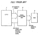
- a conventional CD-ROM device includes a central processing unit (CPU), a signal processing unit and a random access memory (RAM).
- CPU central processing unit
- RAM random access memory
- the signal processing unit supplies the CPU with an error correction process starting signal.
- the CPU supplies the signal processing unit with an address signal calculated in accordance with the error correction process starting signal.
- the signal processing unit supplies the RAM with the calculated address signal as a RAM address signal, at which stored data are corrected in the RAM.
- EP-A-288 989 discloses an address generating circuit which generates a reading address for reading a buffer memory so that so-called P and Q codes for CD-ROM which have parameters i and g can be decoded.
- the address generating circuit is constructed by a logical circuit which operates in accordance with an arrangement of respective code words, and the address generating circuit generates addresses with respect to a memory in which the data and the parity symbols being added to the data are sequentially stored to decode the errror correcting code which is composed of the data and parity symbols. Data and parity symbols are sequentially read from the memory in the order corresponding to the order for decoding.
- the CD-ROM device comprises a RAM for storing data to be read from a CD-ROM, a CPU for controlling operation of reading data from the CD-ROM and a processing unit for processing signals between the RAM and the CPU.
- a conventional CD-ROM device includes a CPU 7, a signal processing unit 8 and a RAM 9.
- the RAM 9 is stored with data read from a CD-ROM device (not shown).
- the stored data is processed in the signal processing unit 8.
- error data may be stored in the RAM 9.
- the error data is required to be corrected as high in probability as possible.
- an address of the data correction must be generated in the address signal generating circuit.
- the RAM address signal is supplied from the signal processing unit 8 as a result of logic calculation process by the CPU 7, as explained before, so that the probability of error data correction is relatively small, and the CPU 7 is burdened with heavy load including such address generation.
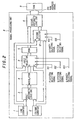
- FIG. 2 shows an address generating circuit in a preferred embodiment.
- the address generating circuit includes a line counter 1 which counts line numbers of addresses, a column counter 2 which counts column numbers thereof, a first arithmetic logic unit 3 which makes a sum of outputs of the line and column counters 1 and 2, a modulator 4 which modulates an output of the first arithmetic logic unit 3, a first selector 11 which selects an output from outputs of the line and column counters 1 and 2 and the modulator 4 in accordance with P- and Q-system selecting signals 101 and 102 and a Q-parity selecting signal 103, a ROM 5 which stores start addresses of the address lines and supplies an output in accordance with an output of the first selector 11, a second selector 12 which selects an output from outputs of the line and column counters 1 and 2 and the ROM 5 in accordance with a Q-parity selecting signal 104 and a system selecting signal 105, and
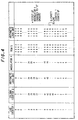
- the ROM 5 stores the start address "0000", “0043”, “0086”, .... of the line addresses at the counted number of "0" of the column counter 2, as described in an address map of the RAM 9 shown in Fig. 3, in which Q- and P-systems of address generation are indicated by arrows.
- the first arithmetic logic unit 3 makes a sum of contents of the line and column counters 1 and 2.
- the modulator 4 generates a modulated number from an output of the first arithmetic logic unit 3. When the input becomes "26”, then the modulator 4 supplies "0", and increases the number again.
- the column number of the column counter 2 becomes "43” or "44”, these numbers are identified as Q-parities, so that the predetermined addresses of "1118" or "1144" are designated in the ROM 5. Then, the column number of the column counter 2 is set to be "0".
- the first selector 11 selects the output of the modulator 4 in accordance with the Q-system selecting signal 101 to be supplied to the ROM 5 when the column number of the address column is at most "42".
- the ROM 5 supplies the start address of the address lines to be supplied to the second arithmetic logic unit 6.
- the second selector 12 selects an output of the column counter 2 in accordance with the system selecting signal 105 to be supplied to the second arithmetic logic unit 6.
- the second arithmetic logic unit 6 makes a sum of the start address read from the ROM 5 and the counted number of the column counter 2 to be supplied to the RAM 9 as the RAM address signal 106.
- the first selector 11 selects the output of the column counter 2 to be supplied to the ROM 5 in accordance with the Q-parity selecting signal 103, so that the ROM 5 supplies the addresses of "1118” or "1144" to the second arithmetic logic unit 6, respectively.
- the second selector 12 selects the output of the line counter 1 to be supplied to the second arithmetic logic unit 6 in accordance with the Q-parity selecting signal 104.
- the second arithmetic logic unit 6 makes a sum of the predetermined address of "1118” or "1144" and the counted number of the line counter 1 to be supplied to the RAM 9 as the RAM address signal 106.
- the first selector 11 selects the output of the line counter 1 in accordance with the P-system selecting signal 101 to be supplied to the ROM 5 when the column number of the address column is at most "42".
- the ROM 5 supplies the start address of the address lines to be supplied to the second arithmetic logic unit 6.
- the second selector 12 selects an output of the column counter 2 in accordance with the system selecting signal 105 to be supplied to the second arithmetic logic unit 6.
- the second arithmetic logic unit 6 makes a sum of the start address read from the ROM 5 and the counted number of the column counter 2 to be supplied to the RAM 9 as the RAM address signal 106.
- the signal processing unit 8 includes the address generating circuit as explained above, so that the RAM address signal 106 is directly supplied to the RAM 9 from the signal processing unit 8 without using the CPU. Therefore, there requires fewer steps to generate addresses than those required in the conventional CD-ROM device, so that the probability of the error correction increases. Further, the load of the CPU is reduced, so that the CPU can exhibit its performance properly.
Landscapes
- Engineering & Computer Science (AREA)
- Theoretical Computer Science (AREA)
- Quality & Reliability (AREA)
- Physics & Mathematics (AREA)
- General Engineering & Computer Science (AREA)
- General Physics & Mathematics (AREA)
- Signal Processing (AREA)
- Error Detection And Correction (AREA)
- Signal Processing For Digital Recording And Reproducing (AREA)
Claims (2)
- Circuit de génération d'adresses pour générer des adresses d'une RAM adapté à la correction d'erreur, les adresses de ladite RAM étant représentées par une carte d'adresses disposée en lignes et en colonnes permettant la génération d'adresses de systèmes P et Q, ledit circuit comprenant :- un compteur de lignes (1) pour compter des numéros de lignes d'adresses de ladite carte d'adresses;- un compteur de colonnes (2) pour compter des numéros de colonnes d'adresses de ladite carte d'adresses (9);- un premier circuit logique (3) pour faire une somme des sorties desdits compteurs de lignes et de colonnes (1, 2);- un modulateur (4) pour moduler une sortie dudit premier circuit logique (3) en tant que nombre d'entrée pour fournir un nombre de sortie modulé, ledit nombre de sortie modulé étant égal audit nombre d'entrée lorsque ledit nombre d'entrée est inférieur à un nombre prédéterminé, et ledit nombre de sortie modulé étant un nombre obtenu en soustrayant ledit nombre prédéterminé ou n fois ledit nombre prédéterminé dudit nombre d'entrée (n = 1, 2, ...) lorsque ledit nombre d'entrée est supérieur ou égal audit nombre prédéterminé, ledit nombre de sortie étant compris entre 0 et ledit nombre prédéterminé moins 1;- un premier sélecteur (11) pour choisir une sortie parmi les sorties desdits compteurs de lignes et de colonnes (1, 2) et ledit modulateur (4) selon que les adresses du système P ou Q sont générées;- une ROM (5) dans laquelle les adresses de début pour toutes les lignes d'adresses de ladite carte d'adresses sont mémorisées et qui est adressée par la sortie dudit premier sélecteur (11);- un second sélecteur (12) pour choisir une sortie parmi les sorties desdits compteurs de lignes et de colonnes (1, 2) selon que les adresses du système P ou Q sont générées; et- un second circuit logique (6) pour faire une somme des sorties de ladite ROM (5) et dudit second sélecteur (12), qui doit être fournie à ladite RAM (9) en tant qu'adresse.
- Dispositif CD-ROM, comprenant :- une RAM (9) adaptée à la correction d'erreur et pour mémoriser des données qui doivent être lues depuis un CD-ROM, les adresses de ladite RAM étant représentées par une carte d'adresses disposée en lignes et en colonnes permettant la génération d'adresses de systèmes P et Q;- une UC (7) pour commander l'opération de lecture de données depuis ledit CD-ROM; et- une unité de traitement de signal (8) pour traiter des signaux entre ladite RAM (9) et ladite UC (7);caractérisé en ce que ladite unité de traitement de signal (8) comprend un circuit de génération d'adresses qui comprend un compteur de lignes (1) pour compter des numéros de lignes d'adresses de ladite carte d'adresses (9); un compteur de colonnes (12) pour compter des numéros de colonnes d'adresses de ladite carte d'adresses (9); un premier circuit logique (3) pour faire une somme des sorties desdits compteurs de lignes et de colonnes (1, 2); un modulateur (4) pour moduler une sortie dudit premier circuit logique (3) en tant que nombre d'entrée pour fournir un nombre de sortie modulé, ledit nombre de sortie modulé étant égal audit nombre d'entrée lorsque ledit nombre d'entrée est inférieur à un nombre prédéterminé, et ledit nombre de sortie modulé étant un nombre obtenu en soustrayant ledit nombre prédéterminé ou n fois ledit nombre prédéterminé dudit nombre d'entrée (n = 1, 2, ...) lorsque ledit nombre d'entrée est supérieur ou égal audit nombre prédéterminé, ledit nombre de sortie étant compris entre 0 et ledit nombre prédéterminé moins 1; un premier sélecteur (11) pour choisir une sortie parmi les sorties desdits compteurs de lignes et de colonnes (1, 2) et ledit modulateur (4) selon que les adresses du système P ou Q sont générées; une ROM (5) dans laquelle les adresses de début pour toutes les lignes d'adresses de ladite carte d'adresses sont mémorisées et qui est adressée par la sortie dudit premier sélecteur (11); un second sélecteur (12) pour choisir une sortie parmi les sorties desdits compteurs de lignes et de colonnes (1, 2) selon que les adresses du système P ou Q sont générées; et un second circuit logique (6) pour faire une somme des sorties de ladite ROM (5) et dudit second sélecteur (12), qui doit être fournie à ladite RAM (9) en tant qu'adresse.
Applications Claiming Priority (2)
| Application Number | Priority Date | Filing Date | Title |
|---|---|---|---|
| JP314731/90 | 1990-11-19 | ||
| JP2314731A JP2781658B2 (ja) | 1990-11-19 | 1990-11-19 | アドレス生成回路とそれを用いたcd―rom装置 |
Publications (3)
| Publication Number | Publication Date |
|---|---|
| EP0487064A2 EP0487064A2 (fr) | 1992-05-27 |
| EP0487064A3 EP0487064A3 (en) | 1992-09-23 |
| EP0487064B1 true EP0487064B1 (fr) | 1997-02-05 |
Family
ID=18056897
Family Applications (1)
| Application Number | Title | Priority Date | Filing Date |
|---|---|---|---|
| EP91119784A Expired - Lifetime EP0487064B1 (fr) | 1990-11-19 | 1991-11-19 | Circuit pour générer des adresses et dispositif CD-ROM utilisant un tel circuit |
Country Status (4)
| Country | Link |
|---|---|
| US (1) | US5524229A (fr) |
| EP (1) | EP0487064B1 (fr) |
| JP (1) | JP2781658B2 (fr) |
| DE (1) | DE69124574T2 (fr) |
Families Citing this family (2)
| Publication number | Priority date | Publication date | Assignee | Title |
|---|---|---|---|---|
| JP2881092B2 (ja) * | 1993-05-25 | 1999-04-12 | 富士通株式会社 | 可換記憶媒体のファイル管理方法 |
| EP1795992B1 (fr) * | 2002-07-30 | 2018-01-24 | Fujitsu Limited | Procédé et appareil de reproduction d'informations utilisant module de sécurité |
Family Cites Families (13)
| Publication number | Priority date | Publication date | Assignee | Title |
|---|---|---|---|---|
| JPS5279628A (en) * | 1975-12-25 | 1977-07-04 | Casio Comput Co Ltd | Information reading processing equipment |
| JPH07101543B2 (ja) * | 1984-03-24 | 1995-11-01 | ソニー株式会社 | エラー訂正符号化方法 |
| EP0156440B1 (fr) * | 1984-03-24 | 1990-01-24 | Koninklijke Philips Electronics N.V. | Méthode de transmission d'information avec correction d'erreurs des mots de données, méthode de décodage de correction d'erreurs pour les mots de données, un appareil de transmission d'information utilisant cette méthode, un appareil pour décoder l'information utilisant cette méthode et un dispositif utilisant un tel appareil |
| JPS60213132A (ja) * | 1984-04-06 | 1985-10-25 | Nec Corp | デイジタル信号処理装置 |
| JP2557340B2 (ja) * | 1984-10-31 | 1996-11-27 | 株式会社東芝 | デジタル再生装置におけるデインタ−リ−ブ処理用メモリの制御方法 |
| JPH0640420B2 (ja) * | 1985-02-27 | 1994-05-25 | 株式会社日立製作所 | Pcm再生装置 |
| GB2184268B (en) * | 1985-12-13 | 1989-11-22 | Anamartic Ltd | Fault tolerant memory system |
| JPS6359221A (ja) * | 1986-08-29 | 1988-03-15 | Nec Home Electronics Ltd | デインタリ−ブ回路 |
| JPS63181169A (ja) * | 1987-01-21 | 1988-07-26 | Matsushita Electric Ind Co Ltd | インタ−リ−ブデインタ−リ−ブ装置 |
| JP2713902B2 (ja) * | 1987-04-28 | 1998-02-16 | 三洋電機株式会社 | アドレス発生回路 |
| JP2829963B2 (ja) * | 1988-05-16 | 1998-12-02 | ソニー株式会社 | ディジタルデータ記録/再生装置 |
| US5257271A (en) * | 1989-07-29 | 1993-10-26 | Sony Corporation | Sample data transmission apparatus |
| KR930000994B1 (ko) * | 1990-08-09 | 1993-02-12 | 삼성전자 주식회사 | Cd-rom 데이타 버퍼링 및 독출용 어드레스 발생방법 및 회로 |
-
1990
- 1990-11-19 JP JP2314731A patent/JP2781658B2/ja not_active Expired - Lifetime
-
1991
- 1991-11-19 EP EP91119784A patent/EP0487064B1/fr not_active Expired - Lifetime
- 1991-11-19 DE DE69124574T patent/DE69124574T2/de not_active Expired - Fee Related
-
1995
- 1995-03-30 US US08/414,044 patent/US5524229A/en not_active Expired - Fee Related
Also Published As
| Publication number | Publication date |
|---|---|
| EP0487064A2 (fr) | 1992-05-27 |
| US5524229A (en) | 1996-06-04 |
| JP2781658B2 (ja) | 1998-07-30 |
| DE69124574D1 (de) | 1997-03-20 |
| DE69124574T2 (de) | 1997-09-04 |
| JPH04184769A (ja) | 1992-07-01 |
| EP0487064A3 (en) | 1992-09-23 |
Similar Documents
| Publication | Publication Date | Title |
|---|---|---|
| US5059976A (en) | Coding method of image information | |
| US6563956B1 (en) | Method and apparatus for compressing data string | |
| US4564944A (en) | Error correcting scheme | |
| US4570221A (en) | Apparatus for sorting data words on the basis of the values of associated parameters | |
| JPS632370B2 (fr) | ||
| EP0487064B1 (fr) | Circuit pour générer des adresses et dispositif CD-ROM utilisant un tel circuit | |
| EP0608848B1 (fr) | Processeur pour codage cyclique et pour code de vérification de redondance cyclique | |
| US5155734A (en) | Error correcting device | |
| USRE35781E (en) | Coding method of image information | |
| US6003110A (en) | Method and apparatus for converting memory addresses into memory selection signals | |
| EP0822481B1 (fr) | Diviseur à constant | |
| EP0408362A2 (fr) | Dispositif de traitement de code pour le détection d'erreurs | |
| JPS58197557A (ja) | メツセ−ジ管理方式 | |
| JPH0426563B2 (fr) | ||
| US20020076113A1 (en) | Image coding device | |
| KR100216045B1 (ko) | 프로그램형 제어기의 비트 연산 처리방법 및 그 장치 | |
| JPH1091715A (ja) | バーコード読取装置 | |
| JP2998532B2 (ja) | 二次元符号化テーブルのアドレス生成回路 | |
| JP2684995B2 (ja) | 命令デコーダ回路 | |
| JPH06268528A (ja) | 可変長符号復号器 | |
| JP2002109535A (ja) | ヒストグラム算出回路 | |
| JPH0731635B2 (ja) | 情報処理装置 | |
| SU1633497A1 (ru) | Устройство дл обнаружени и исправлени ошибок в кодовой последовательности | |
| JPH11102250A (ja) | 疑似nキーロールオーバキーボード入力装置と処理方法 | |
| JPH01200439A (ja) | 未受付要求優先回路 |
Legal Events
| Date | Code | Title | Description |
|---|---|---|---|
| PUAI | Public reference made under article 153(3) epc to a published international application that has entered the european phase |
Free format text: ORIGINAL CODE: 0009012 |
|
| AK | Designated contracting states |
Kind code of ref document: A2 Designated state(s): DE FR GB |
|
| 17P | Request for examination filed |
Effective date: 19920515 |
|
| PUAL | Search report despatched |
Free format text: ORIGINAL CODE: 0009013 |
|
| AK | Designated contracting states |
Kind code of ref document: A3 Designated state(s): DE FR GB |
|
| 17Q | First examination report despatched |
Effective date: 19940802 |
|
| GRAG | Despatch of communication of intention to grant |
Free format text: ORIGINAL CODE: EPIDOS AGRA |
|
| GRAH | Despatch of communication of intention to grant a patent |
Free format text: ORIGINAL CODE: EPIDOS IGRA |
|
| GRAH | Despatch of communication of intention to grant a patent |
Free format text: ORIGINAL CODE: EPIDOS IGRA |
|
| GRAA | (expected) grant |
Free format text: ORIGINAL CODE: 0009210 |
|
| AK | Designated contracting states |
Kind code of ref document: B1 Designated state(s): DE FR GB |
|
| REF | Corresponds to: |
Ref document number: 69124574 Country of ref document: DE Date of ref document: 19970320 |
|
| ET | Fr: translation filed | ||
| PLBE | No opposition filed within time limit |
Free format text: ORIGINAL CODE: 0009261 |
|
| STAA | Information on the status of an ep patent application or granted ep patent |
Free format text: STATUS: NO OPPOSITION FILED WITHIN TIME LIMIT |
|
| 26N | No opposition filed | ||
| REG | Reference to a national code |
Ref country code: GB Ref legal event code: IF02 |
|
| PGFP | Annual fee paid to national office [announced via postgrant information from national office to epo] |
Ref country code: FR Payment date: 20021108 Year of fee payment: 12 |
|
| PGFP | Annual fee paid to national office [announced via postgrant information from national office to epo] |
Ref country code: GB Payment date: 20021113 Year of fee payment: 12 |
|
| PGFP | Annual fee paid to national office [announced via postgrant information from national office to epo] |
Ref country code: DE Payment date: 20021121 Year of fee payment: 12 |
|
| PG25 | Lapsed in a contracting state [announced via postgrant information from national office to epo] |
Ref country code: GB Free format text: LAPSE BECAUSE OF NON-PAYMENT OF DUE FEES Effective date: 20031119 |
|
| PG25 | Lapsed in a contracting state [announced via postgrant information from national office to epo] |
Ref country code: DE Free format text: LAPSE BECAUSE OF NON-PAYMENT OF DUE FEES Effective date: 20040602 |
|
| GBPC | Gb: european patent ceased through non-payment of renewal fee |
Effective date: 20031119 |
|
| PG25 | Lapsed in a contracting state [announced via postgrant information from national office to epo] |
Ref country code: FR Free format text: LAPSE BECAUSE OF NON-PAYMENT OF DUE FEES Effective date: 20040730 |
|
| REG | Reference to a national code |
Ref country code: FR Ref legal event code: ST |