EP0487640B1 - Kondensatorlaminat für halbleiterkarte - Google Patents
Kondensatorlaminat für halbleiterkarte Download PDFInfo
- Publication number
- EP0487640B1 EP0487640B1 EP19900913653 EP90913653A EP0487640B1 EP 0487640 B1 EP0487640 B1 EP 0487640B1 EP 19900913653 EP19900913653 EP 19900913653 EP 90913653 A EP90913653 A EP 90913653A EP 0487640 B1 EP0487640 B1 EP 0487640B1
- Authority
- EP
- European Patent Office
- Prior art keywords
- printed circuit
- capacitor laminate
- circuit board
- capacitive
- devices
- Prior art date
- Legal status (The legal status is an assumption and is not a legal conclusion. Google has not performed a legal analysis and makes no representation as to the accuracy of the status listed.)
- Expired - Lifetime
Links
Images


Classifications
-
- H—ELECTRICITY
- H05—ELECTRIC TECHNIQUES NOT OTHERWISE PROVIDED FOR
- H05K—PRINTED CIRCUITS; CASINGS OR CONSTRUCTIONAL DETAILS OF ELECTRIC APPARATUS; MANUFACTURE OF ASSEMBLAGES OF ELECTRICAL COMPONENTS
- H05K1/00—Printed circuits
- H05K1/16—Printed circuits incorporating printed electric components, e.g. printed resistors, capacitors or inductors
- H05K1/162—Printed circuits incorporating printed electric components, e.g. printed resistors, capacitors or inductors incorporating printed capacitors
-
- H—ELECTRICITY
- H10—SEMICONDUCTOR DEVICES; ELECTRIC SOLID-STATE DEVICES NOT OTHERWISE PROVIDED FOR
- H10W—GENERIC PACKAGES, INTERCONNECTIONS, CONNECTORS OR OTHER CONSTRUCTIONAL DETAILS OF DEVICES COVERED BY CLASS H10
- H10W44/00—Electrical arrangements for controlling or matching impedance
- H10W44/601—Capacitive arrangements
-
- H—ELECTRICITY
- H05—ELECTRIC TECHNIQUES NOT OTHERWISE PROVIDED FOR
- H05K—PRINTED CIRCUITS; CASINGS OR CONSTRUCTIONAL DETAILS OF ELECTRIC APPARATUS; MANUFACTURE OF ASSEMBLAGES OF ELECTRICAL COMPONENTS
- H05K1/00—Printed circuits
- H05K1/02—Details
- H05K1/03—Use of materials for the substrate
- H05K1/0313—Organic insulating material
- H05K1/0353—Organic insulating material consisting of two or more materials, e.g. two or more polymers, polymer + filler, + reinforcement
- H05K1/0366—Organic insulating material consisting of two or more materials, e.g. two or more polymers, polymer + filler, + reinforcement reinforced, e.g. by fibres, fabrics
-
- H—ELECTRICITY
- H05—ELECTRIC TECHNIQUES NOT OTHERWISE PROVIDED FOR
- H05K—PRINTED CIRCUITS; CASINGS OR CONSTRUCTIONAL DETAILS OF ELECTRIC APPARATUS; MANUFACTURE OF ASSEMBLAGES OF ELECTRICAL COMPONENTS
- H05K2201/00—Indexing scheme relating to printed circuits covered by H05K1/00
- H05K2201/02—Fillers; Particles; Fibers; Reinforcement materials
- H05K2201/0203—Fillers and particles
- H05K2201/0206—Materials
- H05K2201/0209—Inorganic, non-metallic particles
-
- H—ELECTRICITY
- H05—ELECTRIC TECHNIQUES NOT OTHERWISE PROVIDED FOR
- H05K—PRINTED CIRCUITS; CASINGS OR CONSTRUCTIONAL DETAILS OF ELECTRIC APPARATUS; MANUFACTURE OF ASSEMBLAGES OF ELECTRICAL COMPONENTS
- H05K2201/00—Indexing scheme relating to printed circuits covered by H05K1/00
- H05K2201/03—Conductive materials
- H05K2201/0332—Structure of the conductor
- H05K2201/0335—Layered conductors or foils
- H05K2201/0355—Metal foils
-
- H—ELECTRICITY
- H05—ELECTRIC TECHNIQUES NOT OTHERWISE PROVIDED FOR
- H05K—PRINTED CIRCUITS; CASINGS OR CONSTRUCTIONAL DETAILS OF ELECTRIC APPARATUS; MANUFACTURE OF ASSEMBLAGES OF ELECTRICAL COMPONENTS
- H05K2201/00—Indexing scheme relating to printed circuits covered by H05K1/00
- H05K2201/09—Shape and layout
- H05K2201/09209—Shape and layout details of conductors
- H05K2201/0929—Conductive planes
- H05K2201/09309—Core having two or more power planes; Capacitive laminate of two power planes
-
- H—ELECTRICITY
- H05—ELECTRIC TECHNIQUES NOT OTHERWISE PROVIDED FOR
- H05K—PRINTED CIRCUITS; CASINGS OR CONSTRUCTIONAL DETAILS OF ELECTRIC APPARATUS; MANUFACTURE OF ASSEMBLAGES OF ELECTRICAL COMPONENTS
- H05K3/00—Apparatus or processes for manufacturing printed circuits
- H05K3/46—Manufacturing multilayer circuits
- H05K3/4611—Manufacturing multilayer circuits by laminating two or more circuit boards
-
- Y—GENERAL TAGGING OF NEW TECHNOLOGICAL DEVELOPMENTS; GENERAL TAGGING OF CROSS-SECTIONAL TECHNOLOGIES SPANNING OVER SEVERAL SECTIONS OF THE IPC; TECHNICAL SUBJECTS COVERED BY FORMER USPC CROSS-REFERENCE ART COLLECTIONS [XRACs] AND DIGESTS
- Y10—TECHNICAL SUBJECTS COVERED BY FORMER USPC
- Y10T—TECHNICAL SUBJECTS COVERED BY FORMER US CLASSIFICATION
- Y10T428/00—Stock material or miscellaneous articles
- Y10T428/31504—Composite [nonstructural laminate]
- Y10T428/3154—Of fluorinated addition polymer from unsaturated monomers
- Y10T428/31544—Addition polymer is perhalogenated
Definitions
- the present invention relates to a capacitor laminate forming a layer within a capacitive printed circuit board to provide a capacitive function for large numbers of devices mounted or formed on the board and methods of manufacture therefor.
- PCBs Printed circuit boards
- these printed circuit boards have long been formed as laminated structures upon which large numbers of devices such as integrated circuits are mounted or formed for use in a wide variety of electronic applications.
- these printed circuit boards have been formed with internal power and ground planes, or conductive sheets, the various devices including traces or electrical connections with both the power and ground planes for facilitating their operation such as it is known, for example, from EP-A-0 086 961.
- capacitors have been found effective to reduce or, in other words, to smooth the undesirable voltage fluctuations referred to above.
- surface or bypass capacitors have not always been effective in all applications.
- the capacitors themselves tend to affect "response" of the integrated circuits or other devices because they have not only a capacitive value but an inductive value as well. It is, of course, well known that inductance arises because of currents passing through conductors such as the traces or connectors coupling the capacitors with the devices or power and ground planes.
- the integrated circuits or other devices are a primary source of radiated energy creating noise from voltage fluctuations in the printed circuit boards. Different characteristics are commonly observed for such devices operating at different speeds or frequencies. Accordingly, the PCBs and device arrays as well as associated capacitors must commonly be designed to assure necessary noise suppression at both high and low speed operation.
- the Sisler concept overcame the problem of providing individual surface capacitors for large numbers of devices or integrated circuits on the PCB by making the PCB itself a capacitive element capable of providing a capacitive function for the various integrated circuits and/or devices. More specifically, the Sisler concept contemplated forming one or more capacitive layers internally within the PCB, the conductive sheets on the capacitive layers preferably forming the power and ground planes of the PCB.
- the Sisler design provided a number of possible important advantages in PCB design. Initially, it entirely avoided the need for most if not all of the surface capacitors on the PCB. At the same time, with the capacitive layer also forming the power and ground planes for the PCB, the Sisler design reduced the number of electrical connectors associated with the integrated circuits and/or devices by approximately 50%.
- the Sisler design contemplated the need for assigning or allotting localized areas or portions of the internal capacitance layer or layers to each of the individual devices and/or integrated circuits.
- the Sisler design contemplated the need for capacitive layers with dielectric sheets and conductive sheets of greatly reduced thicknesses and/or very high dielectric constants generally beyond the capabilities of the existing state of the art.
- the Sisler concept contemplated a number of approaches for achieving the necessary capacitive values because of the design parameters discussed above.
- the Sisler concept required very thin dielectric sheets on the order of no more than about 0.00125 cm (0.5 mils) with the dielectric material having a dielectric constant as high as 200.
- the concept of the present invention was developed as an analogy to observed freeway traffic. It was noted that, during rush hour, large numbers of vehicles attempted to occupy the same "transmission" space and this resulted in the traffic speed being greatly reduced if not brought to a halt at times. By contrast, it was observed that, during ordinary non-rush times, different vehicles traveled along the same transmission channels at different times. Thus, the vehicles did not impede one another and they were able to travel at relatively high speeds.
- the devices tend to fire or operate over different intervals of time so that they can, in effect, employ the same capacitor area of the capacitor laminate because of the novel principle of borrowed capacitance as described above.
- the concept of borrowed capacitance is made possible in a capacitor laminate, provided by the present invention as a layer in the laminated printed circuit board, by following two principles. Initially, the dielectric constant for the dielectric material is selected so that a substantially greater proportional area of the capacitor is necessary to accommodate operation of each device and/or integrated circuit. At the same time, the conductive sheets on opposite sides of the dielectric sheet are provided with sufficient conductance, preferably by increasing the relative thickness of the conductive sheets, in order to assure adequate electron or current flow for permitting the devices and/or integrated circuits to take advantage of increased capacitance resulting from the borrowed capacitance concept of the invention.
- the above design considerations initially permit the material of the dielectric sheet to be selected within existing state-of-the-art parameters while also having an adequate thickness to ensure structural rigidity of the capacitor laminate.
- the increased thickness of the dielectric sheet and the conductor sheets made possible by the present invention, permits the capacitor element or layer to be formed as a laminate of existing sheets of conductive material and dielectric material in order to greatly facilitate manufacture of the capacitor element, that is, as a capacitor laminate.
- PCB printed circuit board
- capacitor laminate included within the multiple layers of the laminated board
- devices such as integrated circuits being mounted or formed on the board and operatively coupled with the capacitor laminate (or multiple capacitor laminates) to provide a capacitive function employing borrowed or shared capacitance as described above.
- Each capacitor laminate includes two sheets of conductive material and an intermediate sheet of dielectric material laminated together as a structurally rigid assembly facilitating its inclusion within the printed circuit board.
- the dielectric material has selected values of thickness and dielectric constant enabling each of the devices or integrated circuit to function in random operation through the concept of borrowed capacitance of the present invention.
- the sheets of conductive material similarly have a minimum conductance value for permitting adequate current flow necessary to provide each individual device with sufficient borrowed capacitance for its proper operation.
- the capacitor laminate is contemplated to include the power and ground planes within the printed circuit board in order to take advantage of design considerations discussed above.
- multiple capacitor laminates may be arranged in spaced apart relation within the PCB for further increased capacitance.
- both the dielectric sheet and the conductive sheets are selected not only on the basis of minimum thickness for structural rigidity but also on the basis of electrical characteristics to assure necessary capacitance as discussed herein. More specifically, the minimum thickness of the dielectric sheet permits the use of state-of-the-art dielectric materials having a dielectric constant of at least about 4. As is discussed in greater detail below, dielectric materials having a dielectric constant in the range of 4 to 5 are readily available and it is possible to form dielectric materials having constants of up to about 10, for example, by forming the dielectric sheets from materials such as ceramic filled epoxies.
- conductance is dependent not only upon the material from which the conductive sheets are formed but also upon the dimensions or more specifically the amount or bulk of conductive material in the sheet. Accordingly, with the conductive sheets being formed from a suitable conductive material such as copper, the dimensions of the sheets are selected in terms of ounces per square foot in order to assure the necessary material for achieving desired conductance.
- the capacitor laminate have a dielectric thickness of at least about 0,00125 cm (0.5 mils) as noted above, more preferably about 0,00375 cm (1.5 mils) with a dielectric constant of about 4.0-5.0, most preferably about 4.7.
- a dielectric sheet formed in accordance with the above limitations can readily be formed from state-of-the-art materials while assuring proper structural rigidity within the sheet.
- the conductive sheets are formed from conductive material, preferably copper, having a minimum thickness of 0,00125 cm or 150 grams per square meter (0.5 mils or about 0.5 ounces per square foot)) as noted above, the conductive sheets more preferably each having a thickness of about 0,0025 cm or 300 grams per square meter (1 mil or about 1.0 ounces per square foot) for an overall thickness in the capacitor laminate of about 0,0089 cm (3.5 mils).
- a preferred embodiment of the invention provides such a desirable capacitor laminate by selecting a dielectric sheet having an initial thickness, prior to lamination, no more than about 4 mils, more preferably no more than about 2 mils and most preferably on the range of approximately 1-1.5 mils, selecting two conductive foils each having one surface treated side with surface roughness or surface variation just sufficient to promote adhesion of the one sides of the conductive foils to the dielectric sheet in a resulting capacitor laminate wherein the one surface treated sides of the conductive foils are in intimate contact with opposite sides of the dielectric sheet wherein by the dielectric sheet has a minimum thickness between all opposing surface portions of the conductive foils for enhanced capacitive integrity.
- the invention provides desired capacitive integrity where the capacitor laminate is contemplated for use in capacitive printed circuit boards where the concept of borrowed or shared capacitance is employed in able to permit or facilitate operation of large numbers of devices mounted upon the PCB and coupled to different portions of the capacitor laminate.
- it is necessary to limit the thickness of the dielectric sheet in order to provide necessary capacitance as described in greater detail hereinbelow.
- the capacitor laminate include a dielectric sheet having commonly available dielectric capabilities and a thickness of not more that about 0,005 cm (2 mils), most preferably in the range of about 0,0025-0,00375 cm (1-1.5 mils).
- capacitor laminate is contemplated for use either as a single or multiple layers within a capacitive PCB based on the theory of shared or borrowed capacitance as noted above, it is also necessary to provide a minimum level of conductivity within the conductive foils as discussed elsewhere herein.
- both surfaces of each dielectric foil are similarly surface treated to assure proper adhesion or bonding both within the capacitor laminate and within a laminated capacitive PCB, for example.
- Such applications can readily be met by employing commonly available conductive foil formed by a well known electrodeposition technique so that the resulting conductive foil, usually copper, has a "barrel" side which may also be referred to as a “smooth” side or “shiny” side.
- the other side of the conductive foil is commonly referred to as the “matte” side but is also known as the “tooth” side and is generally characterized by greater surface roughness or surface variation than on the barrel side of the foil.
- Certain grades of such conductive foil have been found suitable for use within the present invention by reversing the orientation of the conductive from that employed in the prior so that the barrel or smooth side with relatively less surface roughness or surface variation is laminated into intimate contact with the dielectric sheet.
- the present invention also contemplates a conductive foil wherein both surfaces of the conductive foil have similar degrees of surface roughness or surface variation so that the indexing step would not be necessary during lamination of the capacitor laminate.
- FIGURE 1 is a plan view of a capacitive printed circuit board constructed according to the present invention.
- FIGURE 2 is an enlarged fragmentary view of a portion of the printed circuit board showing a device such as an integrated circuit mounted on the surface of the printed circuit board and connected with other devices or components and a power source in the board by through-hole connections.
- a device such as an integrated circuit mounted on the surface of the printed circuit board and connected with other devices or components and a power source in the board by through-hole connections.
- FIGURE 3 is a view similar to FIGURE 2 while illustrating a surface mounted device arranged upon the surface of the printed circuit board and connected with other devices or components and a power source in the printed circuit board by surface traces or pads.
- FIGURE 4 is a schematic sectional view of the printed circuit board illustrating connections or traces for a representative device to power and ground planes formed by a capacitor laminate within the printed circuit board according to the present invention.
- FIGURE 5 is a similar schematic sectional view as FIGURE 4 while illustrating multiple capacitor laminates within the printed circuit board.
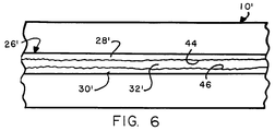
- FIGURE 6 is a photomicrograph of a cross-sectional portion of a capacitive printed circuit board including a capacitor laminate according to the invention.
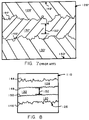
- FIGURE 7 is a prior art representation in the form of a photomicrograph in cross section of a capacitor laminate wherein the matte or tooth sides of two conductive foils are positioned adjacent opposite sides of a dielectric sheet to have a minimum thickness or spacing between all opposing surface portions of the conductive foils of 0,0089 cm (3.5 mils).
- FIGURE 8 is a similar photomicrograph in cross section of a capacitor laminate constructed according to the present invention in order to maintain enhanced capacitive integrity as discussed elsewhere herein.
- a capacitor laminate constructed according to the present invention is described in greater detail below.
- the capacitor laminate of the present invention is designed to facilitate simple manufacture, preferably by lamination of existing separate sheets of a central dielectric sheet of material and conductive sheets on opposite sides thereof, both the dielectric material and conductive material being selected according to the existing state-of-the-art.
- Such a combination has been made possible by the concept of borrowed or shared capacitance as was also summarized above.
- the required thickness of a dielectric layer using standard printed circuit materials and yielding a calculated value for a common bypass capacitor 0,015 microfarads per square centimeter (0.1 microfarads per square inch) results in a nominal thickness of about 0,000053 cm 0.000021 (inches) of dielectric layer in a capacitive layer for a printed circuit board employing two separate capacitive layers in its design.
- This dielectric thickness is obviously not producible from state-of-the-art materials or manufacturing techniques for PCBs at the present time.
- the present invention has also been found to permit improved response of large numbers of devices provided with capacitance by the capacitor laminate of the invention.
- the capacitor laminate of the invention has also been found to permit precise voltage regulation and noise reduction over broad frequency ranges for the devices. In addition to providing such regulation at relatively high frequencies, it has also been found possible to achieve similar voltage regulation and noise reduction at lower frequencies, for example 40 megahertz, by tuning wherein limited numbers of surface capacitors are interconnected with the capacitor laminate as described in greater detail below.
- a capacitive PCB constructed according to the present invention is generally indicated at 10.
- the printed circuit board 10 is of generally conventional construction except for the provision of an internal capacitor laminate as described in greater detail below. Accordingly, external features of the capacitive printed circuit board 10 are only briefly noted, the architecture and design considerations for the printed circuit board otherwise being generally of a type well known to those skilled in the art.
- the capacitive PCB 10 is of a type including large numbers of devices 12 arranged upon its surfaces.
- the devices or components may be arranged upon one or both sides of the board and may include both active devices such as integrated circuits, transistors, etc. Such active devices may even include components such as vacuum tubes or the like.
- the devices 12 may also include passive devices such as capacitors, resistors, inductors, etc.
- an active device such as integrated circuit is indicated at 14 with a passive device, specifically a capacitor being generally indicated at 16.
- These devices are representative of large numbers of devices arranged upon the printed circuit board as generally indicated in FIGURE 1.
- the devices are interconnected to power and ground planes within the printed circuit board and to other devices by through-hole connectors or pins generally indicated at 18.
- two such connectors or pins 18 are illustrated for the capacitor 16 while the integrated circuit 14 is of a 16-pin design including 16 through-hole connectors or pins 18 as illustrated.
- Additional traces may be provided as generally indicated at 20 for facilitating interconnection of the various devices upon the printed circuit board.
- FIGURE 3 Another configuration for a printed circuit board is indicated by the fragmentary representation of FIGURE 3 which similarly illustrates an active device such as an integrated circuit being generally indicated at 14' and illustrated in phantom since it is mounted on the opposite or top surface of the circuit board from the bottom surface illustrated in FIGURE 3.
- a passive device or capacitor 16' is also illustrated in FIGURE 3 preferably mounted on the bottom surface 22 of the printed circuit board. In the surface mounted configuration of FIGURE 3, both the active device 14' and the capacitor 16' are mounted upon surface traces or pads 24.
- the pads 24 facilitate surface mounting of the devices while providing for interconnection of the devices with each other and with a power source such as the internal power and ground planes referred to above by both surface traces and through-hole connectors or pins where necessary.
- the present invention particularly contemplates the use of an internal capacitive layer in the form of the capacitor laminate of the present invention in order to replace large numbers of surface capacitors. Accordingly, although most of the surface capacitors are replaced in the printed circuit board 10 by the capacitor laminate of the invention, a limited number of surface capacitors may still be desirable as illustrated in FIGURES 2 and 3, at least for the purpose of achieving low frequency tuning as discussed in greater detail below.
- FIGURE 4 is a sectional view of the capacitive PCB 10 of FIGURE 1 and illustrates a capacitor laminate 26 constructed according to the present invention and forming an internal capacitive layer within the printed circuit board 10.
- the capacitor laminate 26 includes spaced apart sheets 28 and 30 formed from conductive material, preferably copper, and arranged on opposite sides of a dielectric sheet 32.
- the conductive sheets 28 and 30 form the power and ground planes for the printed circuit board.
- Such a configuration, specifically in terms of the power and ground planes, is well known in the art and no further discussion in that regard is believed necessary.
- a surface mounted device 14' corresponding to the integrated circuit of FIGURE 2, is mounted on the surface of the board in FIGURE 4 and is interconnected with the conductive sheets 28 and 30 by respective power and ground leads 34 and 36.
- the power lead 34 is connected with the conductive sheet 28 while a hole (not shown) is formed in the other conductive sheet 30.
- the ground lead 36 passes through a hole in the conductive sheet 28 while being electrically coupled with the conductive sheet 30. In this manner, the surface device 14' is properly connected with both the power and ground planes.
- Signal traces such as that indicated at 38 are also provided for interconnecting the devices or for making other connections within the PCB as necessary.
- FIGURE 5 another embodiment of a capacitive printed circuit board 10' is illustrated which includes two capacitor laminates 40 and 42.
- a surface mounted device again illustrated at 14' is interconnected with the conductive sheets 28' and 30' by power and ground leads respectively indicated at 34' and 36'.
- the two capacitive layers (or capacitor laminates) provided in FIGURE 5 provide double the capacitance of the single capacitive layer in FIGURE 4, assuming that the overall areas for the capacitor laminates are equal.
- the power and ground planes are effectively provided with twice the amount of conductive material. Accordingly, the design of FIGURE 5 may be employed not only where larger amounts of capacitance is desired but also in higher voltage applications and the like where the power and ground planes are contemplated for carrying either higher current or withstanding larger voltage differentials therebetween.
- FIGURE 6 is a photomicrograph in cross section of the capacitive printed circuit board 10 of FIGURE 1 and is intended to illustrate particular features of the capacitor laminate 26 as discussed in greater detail below.
- capacitor laminate such as that indicated at 26 in FIGURE 4 and a capacitive printed circuit board such as that illustrated at 10 in FIGURE 1
- the individual components of the capacitor laminate are discussed in detail below since they are particularly important to the invention.
- the capacitor laminate 26 is designed to provide necessary capacitance for all or a substantial number of devices mounted upon the surface of the printed circuit board 10. Those devices may be interconnected with the power and ground planes either by separate through-hole pins or by surface traces of the type illustrated respectively in FIGURES 2 and 3.
- the sheet of dielectric material 32 has selected values of thickness and dielectric constant whereby each individual device mounted upon the surface of the printed circuit board is provided with a capacitive function by an allotted portion of the capacitor laminate and also by borrowed capacitance from surrounding portions of the capacitor laminate. Accordingly, as noted above, the capacitive function of the capacitor laminate is dependent upon random firing or operation of the devices since the capacitor laminate 26 provides total capacitance equal to only a portion of the capacitive value necessary for the complete array of devices upon the printed circuit board.
- the conductive sheets 28 and 30 are provided with sufficient conductive material, either in terms of mass per unit area or in terms of thickness, in order to permit adequate electron flow or current flow necessary to provide each individual device with sufficient borrowed capacitance for its proper operation.
- each of the conductive sheets 28 and 30 is formed with a sufficient mass of copper per unit area in order to achieve structural rigidity as noted above and also to permit sufficient electron flow or current flow in accordance with the concept of borrowed capacitance. More specifically, it is contemplated that each of the conductive sheets 28 and 30 be formed with at least about 0.5 ounces of copper per square foot, that mass corresponding generally to a thickness of about 0,00125 cm (0.5 mils), more specifically about 0,00152-0,00175 cm (0.6-0.7 mils). The thickness of the conductive sheets may be increased, for example, in order to meet larger voltage or current carrying capacities for the power and ground planes in a particular application.
- each of the conductive sheets includes about 300-600 grams of copper per square meter (1-2 ounces of copper per square foot), those masses corresponding to thicknesses for the individual sheets in the range of about 0,003-0,006 cm (1.2-2.4 mils). More preferably, the conductive sheets 28 and 30 are formed with about one ounce of copper per square foot or having a thickness in the range of about 0,003-0,0036 cm (1.2-1.4 mils) to achieve optimum performance of the capacitor laminate 26. That amount of copper in each of the conductive sheets is also selected as a minimum for achieving good structural rigidity within the conductive sheets 28 and 30 alone prior to their lamination into the capacitive laminate 26.
- composition and thickness of the dielectric sheet 32 are selected to achieve necessary conductance, again in accordance with the concept of borrowed capacitance, and also to achieve structural rigidity for the dielectric sheet 32, both by itself prior to inclusion within the capacitor laminate 26 as well as for the composite capacitive laminate.
- the present invention preferably contemplates the use of dielectric material having a dielectric constant of at least about 4.
- dielectric compositions for example, from ceramic filled epoxies, with dielectric constants ranging up toward 10 for example.
- the present invention preferably contemplates use of a material with a dielectric constant of at least about 4, more preferably within a range of about 4-5 and most preferably about 4.7, at least for the specific composition contemplated in the preferred embodiment.
- Such a preferred dielectric constant can be achieved by combinations of a woven component and a resin component combined together to form the necessary combination of dielectric constant and structural rigidity.
- the woven component may include polymers such as polytetra fluoroethylene (available under the trade names TEFLON and GORETEX) and epoxi-es.
- the woven components are preferably formed from glass which may be of a quartz variety but is preferably silica, the glass being formed in threads which are then woven together to form sheets filled or impregnated with a selected resin.
- the resins are commonly selected for fire retardant characteristics and may include materials such as cyanate esters, polyimides, kapton materials and other known dielectric materials.
- the resin is preferably an epoxy, again in order to take advantage of the existing state-of-the-art regarding use of such resins in PCB manufacture.
- a dielectric sheet formed from a single woven layer of glass and about 70.0% by weight resin has the preferred dielectric constant of 4.7 as noted above while also exhibiting good structural rigidity at a thickness of about 0,0038 cm (1.5 mils).
- the thickness of the dielectric material in the present invention is selected not only to achieve the desired capacitance but also to assure electrical integrity, particularly the prevention of shorts developing between the conductive sheets 28 and 30 in the capacitor laminate 26.
- Common practice contemplates treatment of the surfaces of the conductive sheets adjacent the dielectric sheet in order to enhance adhesion within the capacitor laminate 26. Such adhesion is necessary not only for structural integrity but also to assure proper electrical performance.
- the adjacent surfaces 44 and 46 of the conductive sheets 28 and 30 respectively are treated typically by deposition of zinc or zinc and copper (a brass alloy), usually by plating, in order to form roughened surfaces best illustrated in the photomicrograph of FIGURE 6. These roughened surfaces provide "tooth" to enhance mechanical bonding to the dielectric material in the sheet 32.
- both the capacitor laminate and a capacitive PCB constructed therefrom are designed with various characteristics, particularly electrical characteristics including capacitance in accordance with the present invention for satisfying the requirements of a variety of applications.
- the capacitor laminate is formed with total capacitance admittedly less than the total capacitance necessary for simultaneous operation of all of the devices on a PCB, at least under optimum conditions. This is made possible through the concept of borrowed capacitance which permits the devices to draw on the necessary capacitive value from the capacitor laminate because of the concept of borrowed capacitance and because of the random operation of the devices.
- the ability of the capacitor laminate constructed according to the present invention to perform its intended function within a capacitive PCB has been found to further illustrate advantages of the concept of borrowed capacitance in that the thickness of the dielectric sheet 32 can be varied as much as ⁇ 10% without affecting the capacitive response of the devices mounted upon the board.
- Such a characteristic is believed to clearly demonstrate that the devices are not functioning purely based upon capacitance in a proportional or allotted amount of the capacitant area. Rather, it is believe that this ability to operate with substantial variation in dielectric thickness indicates an ability of the devices to borrow the amount of capacitance necessary for operation in a given application. In any event, this phenomenon, although possibly not fully understood, is believed to further enhance design variations within the invention.
- the dielectric sheet and conductive sheets are selected in accordance with the preceding discussion for the capacitor laminate.
- the various layers of the capacitor laminate are then assembled and laminated at 21 kilograms per square centimeters (300 pounds per square inch) pressure at a temperature of about 350°F. for about one hour.
- Steel separators are preferably employed adjacent opposite surfaces of the capacitor laminates in order to assure smooth surfaces thereon for facilitating their inclusion in a printed circuit board.
- FIGURE 7 Another aspect of the invention concerning surface treatment or surface characteristics in a capacitor laminate to achieve relatively high capacitance with enhanced capacitive integrity is discussed immediately below with respect to the prior art representation of FIGURE 7 and a similar photomicrograph in cross section of a capacitor laminate constructed according to the present invention.
- a prior art capacitor laminate is generally indicated at 126' while including a single dielectric sheet 132' with conductive foils 128' and 130' laminated to opposite sides of the dielectric sheet 132'.
- each of the conductive foils 128' and 130' had their matte or tooth sides 144' and 146' in intimate contact with the dielectric sheet 132'.
- the barrel or smooth sides 148' and 150' respectively for the conductive foils faced outwardly or away from the dielectric sheet. Such an arrangement was employed in order to maximize adhesion between the two conductive foils and the dielectric sheet.
- the military specification referred to above has been commonly considered a standard for such prior art capacitors.
- the military specification have required that the capacitor withstand a potential of 750 volts per 0.00254 cm (per mil) of dielectric thickness being applied between the conductive foils.
- the military specification required that the dielectric sheet, after being laminated between the conductive foils, have a minimum thickness between any opposing surface portions of the conductive foils of at least 0,0089 cm (3.5 mils).
- Conductive foils such as those indicated at 128' and 130' are commercially supplied by a number of sources including Gould Electronics and Texas Instruments. Conductive foils formed from copper are available from Gould under the trade name "JTC" FOIL as described in Gould Bulletin 88401 published by Gould, Inc., Eastlake, Ohio in March 1989. Other foils available from Gould include those available under the trade names LOW PROFILE "JTC” FOIL and "TC/TC” DOUBLE TREATED COPPER FOIL as described respectively in Bulletin 88406 and Bulletin 88405, both published in March 1989 by Gould, Inc. Those bulletins are incorporated herein in order to provide complete information concerning conductive foils such as those noted above.
- R a and R tm Surface roughness or surface variation of conductive foil such as those noted above is conventionally indicated by foil surface profile measurements, commonly termed R a and R tm . Those values respectively indicate the surface roughness or surface variation for the foil after initial surface treatment by etching and also following further surface treatment in the form of an oxide layer or coating formed from an alloy of copper and zinc.
- the profile measurements R a and R tm are indicated in microns and, for the matte side of the foil, typically range from about 8.0-12.0 microns for the double treated foil referred to above.
- the so-called low profile "JTC" foil typically has a maximum profile measurement in the range of about 6.0-9.0 microns on its matte side.
- the maximum surface profile value that is, up to about 12.0 microns, tends to indicate the maximum penetration of "teeth" on the matte side of the foil into the dielectric sheet during lamination.
- Such a configuration is indicated in FIGURE 7.
- the present invention particularly contemplates capacitor laminates adapted for use in capacitive printed circuit boards with the dielectric sheet of the capacitor laminate having a relative limited thickness in order to achieve a distributed capacitance greater than about 0.1 microfarad.
- the present invention preferably contemplates a capacitor laminate which, in its finally laminated form, has a minimum thickness for the dielectric sheet of about 0,0019-0,00254 cm (0.75-1.0 mils).
- the capacitor laminate was subjected to testing generally in accordance with the military specification noted above. In other words, assuming a dielectric thickness of about 0,00254-0,0038 cm (1-1.5 mils), the capacitor laminates were subjected to a potential of at least 500 volts and as much as 750 volts or 1,000 volts, such testing being carried out to determine the resulting existence of shorts or dielectric failure.
- the present invention contemplates a conductive foil having similar surface roughness or surface variations on both sides in accordance with the preferred conditions set forth above for the drum side or smooth side. The provision of similar surface characteristics on both sides of the conductive foil would eliminate the need for the indexing step referred to immediately above.
- a capacitor laminate constructed according to the present invention could be employed in other applications than the specific capacitive printed circuit board which is a feature of the present invention.
- the capacitor laminate having the preferred surface treatment or surface characteristics as noted above is preferably contemplated for use in a capacitive printed circuit board while enabling the capacitor laminate to function under the theory of borrowed or shared capacitance in order to satisfy capacitance requirements for large numbers of devices mounted upon the PCB.
- the capacitor laminate preferably employs a dielectric sheet having an initial thickness of no more than about 0,01 cm (4 mils), preferably no more than about 0,005 cm 2 mils and most preferably in the range of about 0,0025-0,0037 cm 1-1.5 mils.
- Conductive foils employed in capacitor laminates for a capacitive PCB preferably have conductivity equivalent to a thickness of at least about 0,0025 cm (1 mil) of copper.
- the conductive foils be formed with about 1 ounce of copper per square foot, the resulting thickness of the conductive foil being about 0,003-0,0036 cm (1.2-1.4 mils.)
- the conductive foils are surface treated, preferably upon both sides and at least upon one side arranged adjacent the dielectric sheet with a maximum surface roughness or surface variation corresponding to an R value of about 6.0 microns, preferably about 4.0 microns.
- surface treatment at least of the conductive foil side positioned adjacent the dielectric sheet further enhances capacitive characteristics of the capacitor laminate.
- Such surface treatment preferably includes initial etching and subsequent application of an oxide layer, preferably an alloy of copper and zinc, for example.
- an oxide layer preferably an alloy of copper and zinc, for example.
- other conductive alloys or metals may be employed.
Landscapes
- Engineering & Computer Science (AREA)
- Microelectronics & Electronic Packaging (AREA)
- Parts Printed On Printed Circuit Boards (AREA)
- Production Of Multi-Layered Print Wiring Board (AREA)
- Fixed Capacitors And Capacitor Manufacturing Machines (AREA)
- Heterocyclic Carbon Compounds Containing A Hetero Ring Having Oxygen Or Sulfur (AREA)
- Organic Low-Molecular-Weight Compounds And Preparation Thereof (AREA)
- Inverter Devices (AREA)
Claims (19)
- Kapazitive Leiterplatte (10; 10'; 110) mit einer Mehrzahl von darauf angebrachten oder ausgebildeten Vorrichtungen (12, 14, 16; 12', 14', 16') und umfassend mindestens ein Kondensatorlaminat (26; 26'; 126'), das aus zwei Schichten aus leitendem Material (28, 30; 28', 30'; 128', 130') und einer Zwischenschicht aus dielektrischem Material (32; 32'; 132') besteht, wobei jede dieser Schichten Abmessungen aufweist, die allgemein denjenigen der Leiterplatte (10; 10'; 110) entsprechen, wobei die Schicht aus dielektrischem Material (32; 32'; 132') ausgewählte Werte von Dicke und Dielektrizitätskonstante aufweist, wodurch jede dieser einzelnen, auf der Leiterplatte (10; 10'; 110) angebrachten oder ausgebildeten Vorrichtungen (12, 14, 16; 12', 14', 16') mit einem Kapazitätswert versorgt wird, durch einen zur einzelnen Vorrichtung (12, 14, 16; 12', 14', 16') proportionalen Teil des Kondensatorlaminats (26; 26'; 126') und durch geborgte Kapazität aus anderen, zu anderen Vorrichtungen (12, 14, 16; 12', 14', 16') proportionalen Teilen des Kondensatorlaminats (26; 26'; 126'), wobei die kapazitive Funktion des Kondensatorlaminats (26; 26'; 126') von einer unkorrelierten Auslösung oder Operation der Vorrichtungen (12, 14, 16; 12', 14', 16') abhängig ist, und die Schichten aus leitendem Material (28, 30; 28', 30'; 128', 130') eine Leitfähigkeit aufweisen, um einen Stromfluß zu ermöglichen, der notwendig ist, um jede einzelne der Vorrichtungen (12, 14, 16; 12', 14', 16') mit ausreichend geborgter Kapazität für ihren ordnungsgemäßen Betrieb zu versorgen, wobei das Kondensatorlaminat den größten Teil der benötigten Kapazität für die Mehrzahl von Vorrichtungen bereitstellt.
- Kapazitive Leiterplatte nach Anspruch 1, bei welcher die Schicht aus dielektrischem Material (32; 32'; 132') eine Dicke von mindestens etwa 0,00125 cm (0,5 mils) aufweist, und die Schichten aus leitendem Material (28, 30; 28', 30'; 128', 130') jeweils eine Massenverteilung von mindestens etwa 150 Gramm pro Quadratmeter (0,5 ounces per square foot) aufweisen.
- Kapazitive Leiterplatte nach Anspruch 1, bei welcher mehrere Lagen um dieses Kondensatorlaminat (26; 26'; 126') herumlaminiert sind, und Einrichtungen (18, 24) zum Aufnehmen dieser Mehrzahl von Vorrichtungen (12, 14, 16; 12', 14', 16') in Wirkverbindung mit diesem Kondensatorlaminat (26; 26'; 126') auf der kapazitiven Leiterplatte (10; 10'; 110) ausgebildet sind, und bei welcher Einrichtungen (34, 36; 34', 36') zum Verbinden dieser leitenden Schichten (28, 32; 28', 32'; 128', 132') mit diesen Vorrichtungen (12, 14, 16; 12', 14', 16') vorgesehen sind.
- Kapazitive Leiterplatte nach Anspruch 1, bei welcher das Kondensatorlaminat (26; 26'; 126') eine wesentlich kleinere Kapazität als die für sämtliche der Vorrichtungen (12, 14, 16; 12', 14', 16') auf der Leiterplatte (10; 10'; 110) benötigte kombinierte Kapazität aufweist.
- Kapazitive Leiterplatte nach Anspruch 2, bei welcher die beiden Schichten (28, 32; 28', 32'; 128', 132') aus leitendem Material jeweils innerhalb der kapazitiven Leiterplatte (10; 10'; 110) Netz- und Erde-Ebenen bilden.
- Kapazitive Leiterplatte nach Anspruch 4, weiter umfassend mindestens ein weiteres, in die kapazitive Leiterplatte (10') laminiertes Kondensatorlaminat (26'), und weiter Einrichtungen (34', 36') zum Verbinden von weiteren leitenden Schichten (28', 32') mit den jeweiligen Vorrichtungen (12', 14', 16').
- Kapazitive Leiterplatte nach Anspruch 6, bei welcher die Vorrichtungen (12, 14, 16; 12', 14', 16') von einem Typ sind, welcher über einen Bereich von Arbeitsgeschwindigkeiten oder -frequenzen eine Rauschunterdrückung erforderlich macht, wobei die Wirkung der geborgten Kapazität des Kondensatorlaminats (26, 26') mehreren, jeweils mit den Vorrichtungen (12', 14', 16') verbundenen Kondensatoren ähnelt und dadurch den Kapazitätsbereich innerhalb der kapazitiven Leiterplatte (10') vergrößert.
- Kapazitive Leiterplatte nach einem beliebigen der vorangehenden Ansprüche, bei welcher die Schicht (32, 32'; 132') eine Dicke von etwa 0,00125 bis etwa 0,01 cm (etwa 0,5 mils bis etwa 4 mils), vorzugsweise eine Dicke von etwa 0,0025 bis 0,005 cm (1-2 mils), und eine Dielektrizitätskonstante von etwa 4 bis etwa 10 aufweist.
- Kapazitive Leiterplatte nach einem beliebigen der vorangehenden Ansprüche, bei welcher die Schicht aus dem dielektrischen Material (132') eine Ausgangsdicke von nicht mehr als etwa 0,01 cm (4 mils) aufweist und bei welcher die beiden Schichten aus leitendem Material zwei leitende Folien (128', 130') sind, die jeweils eine oberflächenbehandelte Seite mit einer Oberflächenrauhigkeit oder Oberflächenvariation aufweisen, welche gerade ausreicht, um in einem resultierenden Kondensatorlaminat (126') eine Adhäsion der einen Seiten an der dielektrischen Schicht (132') zu fördern, bei welcher dieses Kondensatorlaminat (126') mit den einen oberflächenbehandelten Seiten der leitenden Folien (128', 130') in inniger Berührung mit gegenüberliegenden Seiten der dielektrischen Schicht (132') ausgebildet ist, wodurch die dielektrische Schicht (132') für eine verbesserte kapazitive Integrität des Kondensatorlaminats (126') zwischen sämtlichen einander gegenüberliegenden Oberflächenbereichen der leitenden Folien (128', 130') eine Mindestdicke aufweist.
- Kapazitive Leiterplatte nach Anspruch 9, bei welcher die Leitfähigkeit für jede leitende Folie (128', 130') mindestens einer Kupferdicke von etwa 0,0025 cm (1 mil) entspricht, und die dielektrische Schicht (132') eine Ausgangsdicke von nicht mehr als etwa 0,005 cm (2 mils) aufweist.
- Kapazitive Leiterplatte nach Anspruch 10, bei welcher die Oberflächenrauhigkeit oder die Oberflächenvariation auf den einen oberflächenbehandelten Seiten jeder leitenden Folie (128', 130') ausgewählt ist, um bei dem besagten Kondensatorlaminat (126') zwischen sämtlichen einander gegenüberliegenden Oberflächenbereichen der leitenden Folien (128', 130') eine Mindestdicke von wenigstens etwa 0,00125 cm (0,5 mils) aufrechtzuerhalten.
- Kapazitive Leiterplatte nach Anspruch 11, bei welcher die Oberflächenrauhigkeit oder Oberflächenvariation auf der einen oberflächenbehandelten Seite jeder leitenden Folie (128', 130') ausgewählt ist, um eine Dicke von etwa 0,001905-0,003175 cm (0,75-1,25 mils) aufrechtzuerhalten.
- Kapazitive Leiterplatte nach Anspruch 1, bei welcher das Kondensatorlaminat weniger als etwa 10 % der für die Mehrzahl von Vorrichtungen benötigten kombinierten Kapazität aufweist.
- Verfahren zur Bildung einer kapazitiven Leiterplatte mit einer Mehrzahl von darauf angebrachten oder ausgebildeten Vorrichtungen, umfassend die Schritte eines Miteinanderverbindens zweier Schichten aus leitendem Material (28, 30; 28', 30'; 128', 130') und einer Zwischenschicht aus dielektrischem Material (32; 32'; 132'), um ein Kondensatorlaminat (26; 26'; 126') als eine strukturell starre Baueinheit zu bilden, Auswählen von Werten von Dicke und Dielektrizitätskonstante für die Schicht aus dielektrischem Material (32; 32'; 132), wodurch jede einzelne, auf der kapazitiven Leiterplatte (10) angebrachte Vorrichtung (12, 14, 16; 12', 14', 16') mit einer Kapazität versorgt wird, durch einen zur einzelnen Vorrichtung (12, 14, 16; 12', 14', 16') proportionalen Teil des Kondensatorlaminats (26; 26'; 126) und durch geborgte Kapazität aus anderen, zu anderen Vorrichtungen proportionalen Teilen des Kondensatorlaminats (26; 26'; 125'), wobei die kapazitive Funktion des Kondensatorlaminats (26; 26'; 126') von der unkorrelierten Auslösung oder Operation der Vorrichtungen (12, 14, 16; 12', 14', 16') abhängig ist, wobei das Kondensatorlaminat den größten Teil des Kapazitätsbedarfs der Vorrichtungen bereitstellt, sowie Auswählen einer Leitfähigkeit für die Schichten aus leitenden Materialien (28, 30; 28', 30'; 128', 130'), um einen Stromfluß zu ermöglichen, der notwendig ist, um jede einzelne dieser Vorrichtungen (12, 14, 16; 12', 14', 16') mit ausreichend geborgter Kapazität für ihren ordnungsgemäßen Betrieb zu versorgen.
- Verfahren nach Anspruch 14, weiter umfassend die Schritte eines Laminierens von mehreren Lagen um das Kondensatorlaminat (26; 26'; 126') herum, und einer Bildung von Einrichtungen (18, 24) zum Aufnehmen einer Mehrzahl von Vorrichtungen (12, 14, 16; 12', 14', 16') auf dieser Leiterplatte (10; 10'; 110') in Wirkverbindung mit dem Kondensatorlaminat (26; 26'; 126'), um eine Kapazität für diese Vorrichtungen (12, 14, 16; 12', 14', 16') bereitzustellen.
- Verfahren nach einem beliebigen der vorangehenden Ansprüche, umfassend die Schritte eines Auswählens einer dielektrischen Schicht (132') mit einer Ausgangsdicke von nicht mehr als etwa 0,1 cm (4 mils), eines Auswählens von zwei leitenden Folien (128', 130'), von denen jede eine oberflächenbehandelte Seite mit einer Oberflächenrauhigkeit oder Oberflächenvariation aufweist, welche gerade ausreicht, um eine Adhäsion der einen Seiten an der dielektrischen Schicht (132') zu fördern, wodurch die dielektrische Schicht (132') für eine verbesserte kapazitive Integrität des Kondensatorlaminats (126') zwischen sämtlichen einander gegenüberliegenden Oberflächenbereichen der leitenden Folien (128', 130') eine Mindestdicke aufweist.
- Verfahren nach Anspruch 16, bei welchem eine Leitfähigkeit für jede leitende Folie (128', 130') mindestens einer Kupferdicke von etwa 0,0025 cm (1 mil) entspricht, und die dielektrische Schicht eine Ausgangsdicke von nicht mehr als etwa 0,005 cm (2 mils) aufweist.
- Verfahren nach Anspruch 17, bei welchem die Oberflächenrauhigkeit oder Oberflächenvariation auf den einen oberflächenbehandelten Seiten jeder leitenden Folie (128', 130') ausgewählt ist, um bei diesem Kondensatorlaminat (126') zwischen sämtlichen einander gegenüberliegenden Oberflächenbereichen der leitenden Folien (128', 130') eine Mindestdicke von wenigstens etwa 0,00125 cm (0,5 mils) aufrechtzuerhalten, und die Oberflächenrauhigkeit oder Oberflächenvariation auf den einen oberflächenbehandelten Seiten jeder leitenden Folie (128', 130') ausgewählt ist, um zwischen sämtlichen einander gegenüberliegenden Oberflächenbereichen der leitenden Folien (128', 130') des gebildeten Kondensatorlaminats (126') eine Dicke von etwa 0,001905-0,003175 cm (0,75 - 1,25 mils) aufrechtzuerhalten.
- Verfahren nach Anspruch 14, bei welchem das Kondensatorlaminat weniger als 10 % der für die Mehrzahl von Vorrichtungen benötigten kombinierten Kapazität aufweist.
Applications Claiming Priority (5)
| Application Number | Priority Date | Filing Date | Title |
|---|---|---|---|
| US07/397,518 US5079069A (en) | 1989-08-23 | 1989-08-23 | Capacitor laminate for use in capacitive printed circuit boards and methods of manufacture |
| US397518 | 1989-08-23 | ||
| US521588 | 1990-05-10 | ||
| US07/521,588 US5155655A (en) | 1989-08-23 | 1990-05-10 | Capacitor laminate for use in capacitive printed circuit boards and methods of manufacture |
| PCT/US1990/004777 WO1991002647A1 (en) | 1989-08-23 | 1990-08-22 | Capacitor laminate for printed circuit board |
Publications (3)
| Publication Number | Publication Date |
|---|---|
| EP0487640A1 EP0487640A1 (de) | 1992-06-03 |
| EP0487640A4 EP0487640A4 (en) | 1993-08-11 |
| EP0487640B1 true EP0487640B1 (de) | 1997-03-19 |
Family
ID=27015899
Family Applications (1)
| Application Number | Title | Priority Date | Filing Date |
|---|---|---|---|
| EP19900913653 Expired - Lifetime EP0487640B1 (de) | 1989-08-23 | 1990-08-22 | Kondensatorlaminat für halbleiterkarte |
Country Status (10)
| Country | Link |
|---|---|
| US (1) | US5155655A (de) |
| EP (1) | EP0487640B1 (de) |
| JP (1) | JP2738590B2 (de) |
| KR (1) | KR100227528B1 (de) |
| AT (1) | ATE150611T1 (de) |
| AU (1) | AU6348590A (de) |
| CA (1) | CA2064784C (de) |
| DE (1) | DE69030260T2 (de) |
| ES (1) | ES2103275T3 (de) |
| WO (1) | WO1991002647A1 (de) |
Cited By (1)
| Publication number | Priority date | Publication date | Assignee | Title |
|---|---|---|---|---|
| US7015260B2 (en) | 2003-06-04 | 2006-03-21 | E.I. Du Pont De Nemours And Company | High temperature polymeric materials containing corona resistant composite filler, and methods relating thereto |
Families Citing this family (139)
| Publication number | Priority date | Publication date | Assignee | Title |
|---|---|---|---|---|
| US5261153A (en) * | 1992-04-06 | 1993-11-16 | Zycon Corporation | In situ method for forming a capacitive PCB |
| US5450046A (en) * | 1992-10-29 | 1995-09-12 | Nec Corporation | Composite microwave circuit module assembly and its connection structure |
| US6728113B1 (en) * | 1993-06-24 | 2004-04-27 | Polychip, Inc. | Method and apparatus for non-conductively interconnecting integrated circuits |
| US6343001B1 (en) | 1996-06-12 | 2002-01-29 | International Business Machines Corporation | Multilayer capacitance structure and circuit board containing the same |
| US5796587A (en) * | 1996-06-12 | 1998-08-18 | International Business Machines Corporation | Printed circut board with embedded decoupling capacitance and method for producing same |
| US6739027B1 (en) | 1996-06-12 | 2004-05-25 | International Business Machines Corporation | Method for producing printed circuit board with embedded decoupling capacitance |
| US5888630A (en) | 1996-11-08 | 1999-03-30 | W. L. Gore & Associates, Inc. | Apparatus and method for unit area composition control to minimize warp in an integrated circuit chip package assembly |
| AU5238898A (en) * | 1996-11-08 | 1998-05-29 | W.L. Gore & Associates, Inc. | Method for reducing via inductance in an electronic assembly and device |
| US5879786A (en) * | 1996-11-08 | 1999-03-09 | W. L. Gore & Associates, Inc. | Constraining ring for use in electronic packaging |
| US5912809A (en) * | 1997-01-21 | 1999-06-15 | Dell Usa, L.P. | Printed circuit board (PCB) including channeled capacitive plane structure |
| US9054094B2 (en) | 1997-04-08 | 2015-06-09 | X2Y Attenuators, Llc | Energy conditioning circuit arrangement for integrated circuit |
| US7336467B2 (en) * | 2000-10-17 | 2008-02-26 | X2Y Attenuators, Llc | Energy pathway arrangement |
| US6687108B1 (en) | 1997-04-08 | 2004-02-03 | X2Y Attenuators, Llc | Passive electrostatic shielding structure for electrical circuitry and energy conditioning with outer partial shielded energy pathways |
| US6603646B2 (en) | 1997-04-08 | 2003-08-05 | X2Y Attenuators, Llc | Multi-functional energy conditioner |
| US6606011B2 (en) * | 1998-04-07 | 2003-08-12 | X2Y Attenuators, Llc | Energy conditioning circuit assembly |
| US7336468B2 (en) | 1997-04-08 | 2008-02-26 | X2Y Attenuators, Llc | Arrangement for energy conditioning |
| US7301748B2 (en) | 1997-04-08 | 2007-11-27 | Anthony Anthony A | Universal energy conditioning interposer with circuit architecture |
| US6636406B1 (en) | 1997-04-08 | 2003-10-21 | X2Y Attenuators, Llc | Universal multi-functional common conductive shield structure for electrical circuitry and energy conditioning |
| US7274549B2 (en) * | 2000-12-15 | 2007-09-25 | X2Y Attenuators, Llc | Energy pathway arrangements for energy conditioning |
| US6498710B1 (en) | 1997-04-08 | 2002-12-24 | X2Y Attenuators, Llc | Paired multi-layered dielectric independent passive component architecture resulting in differential and common mode filtering with surge protection in one integrated package |
| US6018448A (en) * | 1997-04-08 | 2000-01-25 | X2Y Attenuators, L.L.C. | Paired multi-layered dielectric independent passive component architecture resulting in differential and common mode filtering with surge protection in one integrated package |
| US7042703B2 (en) * | 2000-03-22 | 2006-05-09 | X2Y Attenuators, Llc | Energy conditioning structure |
| US20030161086A1 (en) | 2000-07-18 | 2003-08-28 | X2Y Attenuators, Llc | Paired multi-layered dielectric independent passive component architecture resulting in differential and common mode filtering with surge protection in one integrated package |
| US5909350A (en) * | 1997-04-08 | 1999-06-01 | X2Y Attenuators, L.L.C. | Paired multi-layered dielectric independent passive component architecture resulting in differential and common mode filtering with surge protection in one integrated package |
| US6894884B2 (en) * | 1997-04-08 | 2005-05-17 | Xzy Attenuators, Llc | Offset pathway arrangements for energy conditioning |
| US7106570B2 (en) * | 1997-04-08 | 2006-09-12 | Xzy Altenuators, Llc | Pathway arrangement |
| US7110235B2 (en) | 1997-04-08 | 2006-09-19 | Xzy Altenuators, Llc | Arrangement for energy conditioning |
| US6097581A (en) * | 1997-04-08 | 2000-08-01 | X2Y Attenuators, Llc | Paired multi-layered dielectric independent passive component architecture resulting in differential and common mode filtering with surge protection in one integrated package |
| US6650525B2 (en) * | 1997-04-08 | 2003-11-18 | X2Y Attenuators, Llc | Component carrier |
| US6373673B1 (en) | 1997-04-08 | 2002-04-16 | X2Y Attenuators, Llc | Multi-functional energy conditioner |
| US7110227B2 (en) * | 1997-04-08 | 2006-09-19 | X2Y Attenuators, Llc | Universial energy conditioning interposer with circuit architecture |
| US6580595B2 (en) * | 1997-04-08 | 2003-06-17 | X2Y Attenuators, Llc | Predetermined symmetrically balanced amalgam with complementary paired portions comprising shielding electrodes and shielded electrodes and other predetermined element portions for symmetrically balanced and complementary energy portion conditioning |
| US6954346B2 (en) | 1997-04-08 | 2005-10-11 | Xzy Attenuators, Llc | Filter assembly |
| US7321485B2 (en) | 1997-04-08 | 2008-01-22 | X2Y Attenuators, Llc | Arrangement for energy conditioning |
| US6738249B1 (en) | 1997-04-08 | 2004-05-18 | X2Y Attenuators, Llc | Universal energy conditioning interposer with circuit architecture |
| WO1999052210A1 (en) * | 1998-04-07 | 1999-10-14 | X2Y Attenuators, L.L.C. | Component carrier |
| US6068782A (en) * | 1998-02-11 | 2000-05-30 | Ormet Corporation | Individual embedded capacitors for laminated printed circuit boards |
| TW383482B (en) * | 1998-02-13 | 2000-03-01 | United Microelectronics Corp | Multi-layered metal wiring structure for reducing simultaneous switching noise |
| US7427816B2 (en) | 1998-04-07 | 2008-09-23 | X2Y Attenuators, Llc | Component carrier |
| US6608760B2 (en) | 1998-05-04 | 2003-08-19 | Tpl, Inc. | Dielectric material including particulate filler |
| US20040109298A1 (en) * | 1998-05-04 | 2004-06-10 | Hartman William F. | Dielectric material including particulate filler |
| US6616794B2 (en) | 1998-05-04 | 2003-09-09 | Tpl, Inc. | Integral capacitance for printed circuit board using dielectric nanopowders |
| US6631551B1 (en) | 1998-06-26 | 2003-10-14 | Delphi Technologies, Inc. | Method of forming integral passive electrical components on organic circuit board substrates |
| DE19847946A1 (de) * | 1998-10-09 | 2000-04-27 | Siemens Ag | Mehrlagen-Leiterplatte mit integriertem Kondensator |
| US6114015A (en) * | 1998-10-13 | 2000-09-05 | Matsushita Electronic Materials, Inc. | Thin-laminate panels for capacitive printed-circuit boards and methods for making the same |
| US6783620B1 (en) | 1998-10-13 | 2004-08-31 | Matsushita Electronic Materials, Inc. | Thin-laminate panels for capacitive printed-circuit boards and methods for making the same |
| US6215649B1 (en) | 1998-11-05 | 2001-04-10 | International Business Machines Corporation | Printed circuit board capacitor structure and method |
| US6574090B2 (en) | 1998-11-05 | 2003-06-03 | International Business Machines Corporatiion | Printed circuit board capacitor structure and method |
| US6207522B1 (en) * | 1998-11-23 | 2001-03-27 | Microcoating Technologies | Formation of thin film capacitors |
| CA2289239C (en) * | 1998-11-23 | 2010-07-20 | Micro Coating Technologies | Formation of thin film capacitors |
| US6150895A (en) * | 1999-01-25 | 2000-11-21 | Dell Usa, L.P. | Circuit board voltage plane impedance matching |
| US6274224B1 (en) | 1999-02-01 | 2001-08-14 | 3M Innovative Properties Company | Passive electrical article, circuit articles thereof, and circuit articles comprising a passive electrical article |
| US6309805B1 (en) | 1999-09-01 | 2001-10-30 | Morton International, Inc. | Method for securing and processing thin film materials |
| US6212078B1 (en) | 1999-10-27 | 2001-04-03 | Microcoating Technologies | Nanolaminated thin film circuitry materials |
| US6441313B1 (en) * | 1999-11-23 | 2002-08-27 | Sun Microsystems, Inc. | Printed circuit board employing lossy power distribution network to reduce power plane resonances |
| US7113383B2 (en) * | 2000-04-28 | 2006-09-26 | X2Y Attenuators, Llc | Predetermined symmetrically balanced amalgam with complementary paired portions comprising shielding electrodes and shielded electrodes and other predetermined element portions for symmetrically balanced and complementary energy portion conditioning |
| EP1312148A4 (de) | 2000-08-15 | 2009-06-03 | X2Y Attenuators Llc | Elektrodenanordnung zur schaltkreisenergieaufbereitung |
| US6657849B1 (en) | 2000-08-24 | 2003-12-02 | Oak-Mitsui, Inc. | Formation of an embedded capacitor plane using a thin dielectric |
| US6370012B1 (en) | 2000-08-30 | 2002-04-09 | International Business Machines Corporation | Capacitor laminate for use in printed circuit board and as an interconnector |
| JP2002111222A (ja) * | 2000-10-02 | 2002-04-12 | Matsushita Electric Ind Co Ltd | 多層基板 |
| KR100536511B1 (ko) | 2000-10-17 | 2005-12-14 | 엑스2와이 어테뉴에이터스, 엘.엘.씨 | 공통 기준 노드를 갖는 단일 또는 다수의 회로들을 위한 차폐 아말감 및 차폐된 에너지 경로들 및 다른 엘리먼트들 |
| US7193831B2 (en) | 2000-10-17 | 2007-03-20 | X2Y Attenuators, Llc | Energy pathway arrangement |
| KR100388279B1 (ko) * | 2001-01-29 | 2003-06-19 | 전자부품연구원 | Mcm-c 모듈부품의 고주파용 수동소자 내장기판 |
| EP1251530A3 (de) * | 2001-04-16 | 2004-12-29 | Shipley Company LLC | Dielektrisches Laminat für einen Kondensator |
| SG99360A1 (en) * | 2001-04-19 | 2003-10-27 | Gul Technologies Singapore Ltd | A method for forming a printed circuit board and a printed circuit board formed thereby |
| US6577492B2 (en) | 2001-07-10 | 2003-06-10 | 3M Innovative Properties Company | Capacitor having epoxy dielectric layer cured with aminophenylfluorenes |
| JP4079699B2 (ja) | 2001-09-28 | 2008-04-23 | 富士通株式会社 | 多層配線回路基板 |
| US6693793B2 (en) | 2001-10-15 | 2004-02-17 | Mitsui Mining & Smelting Co., Ltd. | Double-sided copper clad laminate for capacitor layer formation and its manufacturing method |
| US6661642B2 (en) | 2001-11-26 | 2003-12-09 | Shipley Company, L.L.C. | Dielectric structure |
| US6819540B2 (en) * | 2001-11-26 | 2004-11-16 | Shipley Company, L.L.C. | Dielectric structure |
| US20030152309A1 (en) * | 2002-02-14 | 2003-08-14 | Howard James Robert | Printed circuit board containing optical elements |
| US7038143B2 (en) | 2002-05-16 | 2006-05-02 | Mitsubishi Denki Kabushiki Kaisha | Wiring board, fabrication method of wiring board, and semiconductor device |
| JP4323137B2 (ja) * | 2002-06-03 | 2009-09-02 | 新光電気工業株式会社 | 基板埋め込み用キャパシタ、基板埋め込み用キャパシタを埋め込んだ回路基板及び基板埋め込み用キャパシタの製造方法 |
| JP3711343B2 (ja) | 2002-06-26 | 2005-11-02 | 株式会社トッパンNecサーキットソリューションズ | 印刷配線板及びその製造方法並びに半導体装置 |
| WO2004010751A1 (ja) * | 2002-07-18 | 2004-01-29 | Hitachi Chemical Co., Ltd. | 多層配線板、およびその製造方法、ならびに半導体装置および無線電子装置 |
| US7180718B2 (en) | 2003-01-31 | 2007-02-20 | X2Y Attenuators, Llc | Shielded energy conditioner |
| JP4226927B2 (ja) * | 2003-02-18 | 2009-02-18 | 三井金属鉱業株式会社 | キャパシタ層形成用の両面銅張積層板の製造方法 |
| WO2005002018A2 (en) | 2003-05-29 | 2005-01-06 | X2Y Attenuators, Llc | Connector related structures including an energy |
| US20060074164A1 (en) * | 2003-12-19 | 2006-04-06 | Tpl, Inc. | Structured composite dielectrics |
| US20060074166A1 (en) * | 2003-12-19 | 2006-04-06 | Tpl, Inc. Title And Interest In An Application | Moldable high dielectric constant nano-composites |
| US20080128961A1 (en) * | 2003-12-19 | 2008-06-05 | Tpl, Inc. | Moldable high dielectric constant nano-composites |
| KR20060120683A (ko) | 2003-12-22 | 2006-11-27 | 엑스2와이 어테뉴에이터스, 엘.엘.씨 | 내부적으로 차폐된 에너지 컨디셔너 |
| US7413815B2 (en) * | 2004-02-19 | 2008-08-19 | Oak-Mitsui Inc. | Thin laminate as embedded capacitance material in printed circuit boards |
| KR100586963B1 (ko) * | 2004-05-04 | 2006-06-08 | 삼성전기주식회사 | 유전체 형성용 조성물, 이로 제조된 캐패시터층 및 이를포함하는 인쇄회로기판 |
| JP4552524B2 (ja) * | 2004-06-10 | 2010-09-29 | パナソニック株式会社 | 複合型電子部品 |
| US20060000542A1 (en) * | 2004-06-30 | 2006-01-05 | Yongki Min | Metal oxide ceramic thin film on base metal electrode |
| JP2006121046A (ja) | 2004-09-24 | 2006-05-11 | Meiko:Kk | 回路基板 |
| US7425760B1 (en) | 2004-10-13 | 2008-09-16 | Sun Microsystems, Inc. | Multi-chip module structure with power delivery using flexible cables |
| US7290315B2 (en) * | 2004-10-21 | 2007-11-06 | Intel Corporation | Method for making a passive device structure |
| US20060099803A1 (en) * | 2004-10-26 | 2006-05-11 | Yongki Min | Thin film capacitor |
| US20060091495A1 (en) * | 2004-10-29 | 2006-05-04 | Palanduz Cengiz A | Ceramic thin film on base metal electrode |
| JP2006147606A (ja) | 2004-11-16 | 2006-06-08 | Nec Toppan Circuit Solutions Inc | シート状コンデンサとその製造方法 |
| US7778038B2 (en) * | 2004-12-21 | 2010-08-17 | E.I. Du Pont De Nemours And Company | Power core devices and methods of making thereof |
| US20060158828A1 (en) * | 2004-12-21 | 2006-07-20 | Amey Daniel I Jr | Power core devices and methods of making thereof |
| US7613007B2 (en) * | 2004-12-21 | 2009-11-03 | E. I. Du Pont De Nemours And Company | Power core devices |
| US7192654B2 (en) * | 2005-02-22 | 2007-03-20 | Oak-Mitsui Inc. | Multilayered construction for resistor and capacitor formation |
| JP2008537843A (ja) | 2005-03-01 | 2008-09-25 | エックストゥーワイ アテニュエイターズ,エルエルシー | 内部で重なり合った調整器 |
| WO2006093831A2 (en) | 2005-03-01 | 2006-09-08 | X2Y Attenuators, Llc | Energy conditioner with tied through electrodes |
| KR100688743B1 (ko) * | 2005-03-11 | 2007-03-02 | 삼성전기주식회사 | 멀티 레이어 커패시터 내장형의 인쇄회로기판의 제조방법 |
| WO2006099297A2 (en) | 2005-03-14 | 2006-09-21 | X2Y Attenuators, Llc | Conditioner with coplanar conductors |
| US7629269B2 (en) * | 2005-03-31 | 2009-12-08 | Intel Corporation | High-k thin film grain size control |
| US7375412B1 (en) | 2005-03-31 | 2008-05-20 | Intel Corporation | iTFC with optimized C(T) |
| US20060220177A1 (en) * | 2005-03-31 | 2006-10-05 | Palanduz Cengiz A | Reduced porosity high-k thin film mixed grains for thin film capacitor applications |
| US20060274478A1 (en) * | 2005-06-06 | 2006-12-07 | Wus Printed Circuit Co. Ltd. | Etched capacitor laminate for reducing electrical noise |
| US7453144B2 (en) * | 2005-06-29 | 2008-11-18 | Intel Corporation | Thin film capacitors and methods of making the same |
| US20070004844A1 (en) * | 2005-06-30 | 2007-01-04 | Clough Robert S | Dielectric material |
| US7621041B2 (en) * | 2005-07-11 | 2009-11-24 | E. I. Du Pont De Nemours And Company | Methods for forming multilayer structures |
| KR100665261B1 (ko) * | 2005-10-13 | 2007-01-09 | 삼성전기주식회사 | 온도변화에 따른 정전용량변화가 작은 복합 유전체 조성물및 이를 이용한 시그널 매칭용 임베디드 캐패시터 |
| US7457132B2 (en) * | 2005-10-20 | 2008-11-25 | Sanmina-Sci Corporation | Via stub termination structures and methods for making same |
| US7504706B2 (en) * | 2005-10-21 | 2009-03-17 | E. I. Du Pont De Nemours | Packaging having an array of embedded capacitors for power delivery and decoupling in the mid-frequency range and methods of forming thereof |
| US7705423B2 (en) * | 2005-10-21 | 2010-04-27 | Georgia Tech Research Corporation | Device having an array of embedded capacitors for power delivery and decoupling of high speed input/output circuitry of an integrated circuit |
| US7456459B2 (en) * | 2005-10-21 | 2008-11-25 | Georgia Tech Research Corporation | Design of low inductance embedded capacitor layer connections |
| TWI295102B (en) * | 2006-01-13 | 2008-03-21 | Ind Tech Res Inst | Multi-functional substrate structure |
| TWI279552B (en) * | 2006-01-18 | 2007-04-21 | Ind Tech Res Inst | Test method of embedded capacitor and test system thereof |
| US7631423B2 (en) * | 2006-02-13 | 2009-12-15 | Sanmina-Sci Corporation | Method and process for embedding electrically conductive elements in a dielectric layer |
| EP1991996A1 (de) | 2006-03-07 | 2008-11-19 | X2Y Attenuators, L.L.C. | Energiekonditionierungsstrukturen |
| US8134084B2 (en) | 2006-06-30 | 2012-03-13 | Shin-Etsu Polymer Co., Ltd. | Noise-suppressing wiring-member and printed wiring board |
| TWI302372B (en) * | 2006-08-30 | 2008-10-21 | Polytronics Technology Corp | Heat dissipation substrate for electronic device |
| JP2007165932A (ja) * | 2007-02-22 | 2007-06-28 | Matsushita Electric Ind Co Ltd | 多層基板 |
| JP6095039B2 (ja) * | 2007-03-10 | 2017-03-15 | サンミナ−エスシーアイ コーポレーション | 内蔵型容量性積層体 |
| US7573721B2 (en) * | 2007-05-17 | 2009-08-11 | Kinsus Interconnect Technology Corp. | Embedded passive device structure and manufacturing method thereof |
| US20090034156A1 (en) * | 2007-07-30 | 2009-02-05 | Takuya Yamamoto | Composite sheet |
| US7733627B2 (en) | 2007-09-24 | 2010-06-08 | Wan-Ling Yu | Structure of embedded capacitor |
| TWI382433B (zh) * | 2007-10-16 | 2013-01-11 | 財團法人工業技術研究院 | 提升自振頻率之電容結構 |
| US20090154127A1 (en) * | 2007-12-18 | 2009-06-18 | Ting-Hao Lin | PCB Embedded Electronic Elements Structure And Method Thereof |
| US8730647B2 (en) * | 2008-02-07 | 2014-05-20 | Ibiden Co., Ltd. | Printed wiring board with capacitor |
| US8083954B2 (en) * | 2008-06-03 | 2011-12-27 | Kinsus Interconnect Technology Corp. | Method for fabricating component-embedded printed circuit board |
| US20110048777A1 (en) * | 2009-08-25 | 2011-03-03 | Chien-Wei Chang | Component-Embedded Printed Circuit Board |
| US8431826B2 (en) | 2010-05-14 | 2013-04-30 | James Robert Howard | Capacitive power and ground plane structure utilizing fractal elements for the reduction of radiated emissions |
| WO2012151738A1 (zh) * | 2011-05-06 | 2012-11-15 | 广东生益科技股份有限公司 | 埋容材料及其制作方法 |
| US8829648B2 (en) | 2012-03-05 | 2014-09-09 | Fuji Xerox Co., Ltd. | Package substrate and semiconductor package |
| KR101771724B1 (ko) * | 2012-04-18 | 2017-08-25 | 삼성전기주식회사 | 적층 세라믹 전자부품 및 이의 제조방법 |
| IN2015DN00730A (de) * | 2012-08-30 | 2015-07-10 | Allison Transm Inc | |
| CN204994111U (zh) | 2013-02-15 | 2016-01-20 | 株式会社村田制作所 | 层叠电路基板 |
| JP6649770B2 (ja) | 2014-02-21 | 2020-02-19 | 三井金属鉱業株式会社 | 内蔵キャパシタ層形成用銅張積層板、多層プリント配線板及び多層プリント配線板の製造方法 |
| DE102014109990B4 (de) * | 2014-07-16 | 2022-10-27 | Infineon Technologies Austria Ag | Messwiderstand mit vertikalem Stromfluss, Halbleiterpackage mit einem Messwiderstand und Verfahren zur Herstellung eines Messwiderstandes |
| WO2017154167A1 (ja) * | 2016-03-10 | 2017-09-14 | 三井金属鉱業株式会社 | 多層積層板及びこれを用いた多層プリント配線板の製造方法 |
| WO2018229675A1 (en) * | 2017-06-13 | 2018-12-20 | 3M Innovative Properties Company | High-voltage impedance assembly |
| KR20240140417A (ko) | 2023-03-16 | 2024-09-24 | 주식회사 삼주전자 | 인쇄회로기판의 제조방법 |
Family Cites Families (48)
| Publication number | Priority date | Publication date | Assignee | Title |
|---|---|---|---|---|
| US2593829A (en) * | 1949-01-13 | 1952-04-22 | Bayer Ag | Electrical capacitor and foil therefor |
| US2740732A (en) * | 1951-07-16 | 1956-04-03 | Sprague Electric Co | Process of bonding a metal film to a thermoplastic sheet and resulting product |
| US3034930A (en) * | 1957-05-10 | 1962-05-15 | Motorola Inc | Printed circuit process |
| US3142047A (en) * | 1960-12-14 | 1964-07-21 | Columbia Broadcasting Systems | Memory plane |
| US3345741A (en) * | 1963-03-14 | 1967-10-10 | Litton Systems Inc | Weldable printed circuit board techniques |
| US3348990A (en) * | 1963-12-23 | 1967-10-24 | Sperry Rand Corp | Process for electrically interconnecting elements on different layers of a multilayer printed circuit assembly |
| US3436819A (en) * | 1965-09-22 | 1969-04-08 | Litton Systems Inc | Multilayer laminate |
| FR1492897A (fr) * | 1966-04-27 | 1967-08-25 | Thomson Houston Comp Francaise | Perfectionnements aux procédés de réalisation de circuits imprimés multicouches et circuits ainsi obtenus |
| US3506482A (en) * | 1967-04-25 | 1970-04-14 | Matsushita Electric Industrial Co Ltd | Method of making printed circuits |
| DE1936899A1 (de) * | 1969-07-19 | 1971-02-04 | Siemens Ag | Baugruppentraeger fuer Steuer- bzw. Regelanlagen |
| US3619743A (en) * | 1970-01-26 | 1971-11-09 | Cornell Dubilier Electric | Impregnated capacitor with all-film dielectrics and at least one foil electrode having a chemically produced pattern of passages for promoting impregnation |
| US3742597A (en) * | 1971-03-17 | 1973-07-03 | Hadco Printed Circuits Inc | Method for making a coated printed circuit board |
| BE795626A (fr) * | 1972-02-25 | 1973-08-20 | Michelin & Cie | Perfectionnements aux enveloppes de pneumatiques |
| US3932932A (en) * | 1974-09-16 | 1976-01-20 | International Telephone And Telegraph Corporation | Method of making multilayer printed circuit board |
| JPS5368870A (en) * | 1976-12-01 | 1978-06-19 | Oki Electric Ind Co Ltd | Multilayer board |
| JPS5440170U (de) * | 1977-08-24 | 1979-03-16 | ||
| FR2402379A1 (fr) * | 1977-08-31 | 1979-03-30 | Cayrol Pierre Henri | Perfectionnements apportes aux circuits imprimes |
| US4211603A (en) * | 1978-05-01 | 1980-07-08 | Tektronix, Inc. | Multilayer circuit board construction and method |
| JPS5687694A (en) * | 1979-12-19 | 1981-07-16 | Nippon Mining Co Ltd | Manufacture of copper foil for printed circuit |
| US4301192A (en) * | 1980-06-02 | 1981-11-17 | Western Electric Co., Inc. | Method for coating thru holes in a printed circuit substrate |
| US4388136A (en) * | 1980-09-26 | 1983-06-14 | Sperry Corporation | Method of making a polyimide/glass hybrid printed circuit board |
| US4522888A (en) * | 1980-12-29 | 1985-06-11 | General Electric Company | Electrical conductors arranged in multiple layers |
| US4417393A (en) * | 1981-04-01 | 1983-11-29 | General Electric Company | Method of fabricating high density electronic circuits having very narrow conductors |
| JPS5932915B2 (ja) * | 1981-07-25 | 1984-08-11 | 「弐」夫 甲斐 | スル−ホ−ルを有する配線基板製造方法 |
| US4494172A (en) * | 1982-01-28 | 1985-01-15 | Mupac Corporation | High-speed wire wrap board |
| US4486738A (en) * | 1982-02-16 | 1984-12-04 | General Electric Ceramics, Inc. | High reliability electrical components |
| US4554732A (en) * | 1982-02-16 | 1985-11-26 | General Electric Company | High reliability electrical components |
| US4633035A (en) * | 1982-07-12 | 1986-12-30 | Rogers Corporation | Microwave circuit boards |
| JPS59101356A (ja) * | 1982-12-01 | 1984-06-11 | 松下電工株式会社 | 銅箔およびそれを用いた電気用積層板 |
| US4543715A (en) * | 1983-02-28 | 1985-10-01 | Allied Corporation | Method of forming vertical traces on printed circuit board |
| JPS59194493A (ja) * | 1983-04-18 | 1984-11-05 | 松下電器産業株式会社 | コンデンサ内蔵型セラミツク多層配線基板 |
| US4560962A (en) * | 1983-08-30 | 1985-12-24 | Burroughs Corporation | Multilayered printed circuit board with controlled 100 ohm impedance |
| JPS6048230U (ja) * | 1983-09-11 | 1985-04-04 | 株式会社村田製作所 | 積層コンデンサ |
| US4642569A (en) * | 1983-12-16 | 1987-02-10 | General Electric Company | Shield for decoupling RF and gradient coils in an NMR apparatus |
| US4554229A (en) * | 1984-04-06 | 1985-11-19 | At&T Technologies, Inc. | Multilayer hybrid integrated circuit |
| JPS60214941A (ja) * | 1984-04-10 | 1985-10-28 | 株式会社 潤工社 | プリント基板 |
| JPS60226197A (ja) * | 1984-04-25 | 1985-11-11 | 株式会社日立製作所 | 電子装置 |
| US4605915A (en) * | 1984-07-09 | 1986-08-12 | Cubic Corporation | Stripline circuits isolated by adjacent decoupling strip portions |
| JPS6132489A (ja) * | 1984-07-24 | 1986-02-15 | 株式会社日立製作所 | 多層印刷回路基板 |
| US4675717A (en) * | 1984-10-09 | 1987-06-23 | American Telephone And Telegraph Company, At&T Bell Laboratories | Water-scale-integrated assembly |
| US4635358A (en) * | 1985-01-03 | 1987-01-13 | E. I. Du Pont De Nemours And Company | Method for forming electrically conductive paths through a dielectric layer |
| US4584627A (en) * | 1985-01-09 | 1986-04-22 | Rogers Corporation | Flat decoupling capacitor and method of manufacture thereof |
| US4636018A (en) * | 1985-06-05 | 1987-01-13 | Amp Incorporated | Elastomeric electrical connector |
| US4739257A (en) * | 1985-06-06 | 1988-04-19 | Automated Electronic Technology, Inc. | Testsite system |
| JPS634689A (ja) * | 1986-06-25 | 1988-01-09 | 松下電工株式会社 | プリント配線板 |
| US4775573A (en) * | 1987-04-03 | 1988-10-04 | West-Tronics, Inc. | Multilayer PC board using polymer thick films |
| JPH01169989A (ja) * | 1987-12-24 | 1989-07-05 | Ngk Insulators Ltd | セラミックグリーンシート |
| US5079069A (en) * | 1989-08-23 | 1992-01-07 | Zycon Corporation | Capacitor laminate for use in capacitive printed circuit boards and methods of manufacture |
-
1990
- 1990-05-10 US US07/521,588 patent/US5155655A/en not_active Expired - Lifetime
- 1990-08-22 WO PCT/US1990/004777 patent/WO1991002647A1/en not_active Ceased
- 1990-08-22 JP JP51274390A patent/JP2738590B2/ja not_active Expired - Lifetime
- 1990-08-22 DE DE69030260T patent/DE69030260T2/de not_active Expired - Lifetime
- 1990-08-22 EP EP19900913653 patent/EP0487640B1/de not_active Expired - Lifetime
- 1990-08-22 AT AT90913653T patent/ATE150611T1/de not_active IP Right Cessation
- 1990-08-22 AU AU63485/90A patent/AU6348590A/en not_active Abandoned
- 1990-08-22 ES ES90913653T patent/ES2103275T3/es not_active Expired - Lifetime
- 1990-08-22 KR KR1019920700416A patent/KR100227528B1/ko not_active Expired - Lifetime
- 1990-08-22 CA CA 2064784 patent/CA2064784C/en not_active Expired - Lifetime
Cited By (1)
| Publication number | Priority date | Publication date | Assignee | Title |
|---|---|---|---|---|
| US7015260B2 (en) | 2003-06-04 | 2006-03-21 | E.I. Du Pont De Nemours And Company | High temperature polymeric materials containing corona resistant composite filler, and methods relating thereto |
Also Published As
| Publication number | Publication date |
|---|---|
| WO1991002647A1 (en) | 1991-03-07 |
| JP2738590B2 (ja) | 1998-04-08 |
| EP0487640A1 (de) | 1992-06-03 |
| ATE150611T1 (de) | 1997-04-15 |
| DE69030260T2 (de) | 1997-10-30 |
| ES2103275T3 (es) | 1997-09-16 |
| DE69030260D1 (de) | 1997-04-24 |
| EP0487640A4 (en) | 1993-08-11 |
| JPH05500136A (ja) | 1993-01-14 |
| CA2064784C (en) | 1998-11-24 |
| US5155655A (en) | 1992-10-13 |
| KR100227528B1 (ko) | 1999-11-01 |
| CA2064784A1 (en) | 1991-02-24 |
| AU6348590A (en) | 1991-04-03 |
Similar Documents
| Publication | Publication Date | Title |
|---|---|---|
| EP0487640B1 (de) | Kondensatorlaminat für halbleiterkarte | |
| US5161086A (en) | Capacitor laminate for use in capacitive printed circuit boards and methods of manufacture | |
| US5079069A (en) | Capacitor laminate for use in capacitive printed circuit boards and methods of manufacture | |
| US5261153A (en) | In situ method for forming a capacitive PCB | |
| US5870274A (en) | Capacitive PCB with internal capacitive laminate | |
| US5796587A (en) | Printed circut board with embedded decoupling capacitance and method for producing same | |
| EP2346310B1 (de) | Mehrschichtige Leiterplatte | |
| US6524352B2 (en) | Method of making a parallel capacitor laminate | |
| US6343001B1 (en) | Multilayer capacitance structure and circuit board containing the same | |
| EP1443811A2 (de) | Hochgeschwindigkeits-Leiterplatte und Verfahren zu ihrer Herstellung | |
| CN1717149B (zh) | 电路化衬底 | |
| US6004657A (en) | Laminated electronic part | |
| CN118338525A (zh) | 布线基板 | |
| WO1994002310A1 (en) | Printed circuit board with internal capacitor | |
| EP1641330A1 (de) | Leiterplatte | |
| CN120825869B (zh) | 一种新能源汽车用高导热低损耗多层pcb及其制备工艺 | |
| JPH07336005A (ja) | フレキシブルプリント配線板及びその製造方法 | |
| KR100528013B1 (ko) | 커패시터를 갖는 인쇄회로기판 | |
| KR19990073126A (ko) | 램버스용인쇄회로기판 | |
| JPH0513559B2 (de) | ||
| JP2000188449A (ja) | 配線基板及びその製造方法 | |
| EP0354341A1 (de) | Zusammengesetzte Struktur zur Verwendung in elektronischen Packungen | |
| JPH02122588A (ja) | 金属板ベースプリント配線板 | |
| JPH03173498A (ja) | ブラインドスルホール多層基板 | |
| JPS62177996A (ja) | 二層プリント回路基板 |
Legal Events
| Date | Code | Title | Description |
|---|---|---|---|
| PUAI | Public reference made under article 153(3) epc to a published international application that has entered the european phase |
Free format text: ORIGINAL CODE: 0009012 |
|
| 17P | Request for examination filed |
Effective date: 19920213 |
|
| AK | Designated contracting states |
Kind code of ref document: A1 Designated state(s): AT BE CH DE DK ES FR GB IT LI LU NL SE |
|
| A4 | Supplementary search report drawn up and despatched |
Effective date: 19930625 |
|
| AK | Designated contracting states |
Kind code of ref document: A4 Designated state(s): AT BE CH DE DK ES FR GB IT LI LU NL SE |
|
| RHK1 | Main classification (correction) |
Ipc: H05K 1/16 |
|
| 17Q | First examination report despatched |
Effective date: 19940502 |
|
| GRAG | Despatch of communication of intention to grant |
Free format text: ORIGINAL CODE: EPIDOS AGRA |
|
| GRAH | Despatch of communication of intention to grant a patent |
Free format text: ORIGINAL CODE: EPIDOS IGRA |
|
| GRAH | Despatch of communication of intention to grant a patent |
Free format text: ORIGINAL CODE: EPIDOS IGRA |
|
| GRAA | (expected) grant |
Free format text: ORIGINAL CODE: 0009210 |
|
| AK | Designated contracting states |
Kind code of ref document: B1 Designated state(s): AT BE CH DE DK ES FR GB IT LI LU NL SE |
|
| PG25 | Lapsed in a contracting state [announced via postgrant information from national office to epo] |
Ref country code: DK Effective date: 19970319 |
|
| REF | Corresponds to: |
Ref document number: 150611 Country of ref document: AT Date of ref document: 19970415 Kind code of ref document: T |
|
| REG | Reference to a national code |
Ref country code: CH Ref legal event code: EP |
|
| REF | Corresponds to: |
Ref document number: 69030260 Country of ref document: DE Date of ref document: 19970424 |
|
| ITF | It: translation for a ep patent filed | ||
| ET | Fr: translation filed | ||
| PG25 | Lapsed in a contracting state [announced via postgrant information from national office to epo] |
Ref country code: LU Free format text: LAPSE BECAUSE OF NON-PAYMENT OF DUE FEES Effective date: 19970822 |
|
| REG | Reference to a national code |
Ref country code: ES Ref legal event code: FG2A Ref document number: 2103275 Country of ref document: ES Kind code of ref document: T3 |
|
| REG | Reference to a national code |
Ref country code: CH Ref legal event code: NV Representative=s name: BUGNION S.A. |
|
| PLBI | Opposition filed |
Free format text: ORIGINAL CODE: 0009260 |
|
| PLBF | Reply of patent proprietor to notice(s) of opposition |
Free format text: ORIGINAL CODE: EPIDOS OBSO |
|
| 26 | Opposition filed |
Opponent name: PHOTO PRINT ELECTRONIC GMBH Effective date: 19971219 Opponent name: SIEMENS AG Effective date: 19971218 |
|
| NLR1 | Nl: opposition has been filed with the epo |
Opponent name: PHOTO PRINT ELECTRONIC GMBH Opponent name: SIEMENS AG |
|
| PLBF | Reply of patent proprietor to notice(s) of opposition |
Free format text: ORIGINAL CODE: EPIDOS OBSO |
|
| PLBQ | Unpublished change to opponent data |
Free format text: ORIGINAL CODE: EPIDOS OPPO |
|
| NLT1 | Nl: modifications of names registered in virtue of documents presented to the patent office pursuant to art. 16 a, paragraph 1 |
Owner name: HADCO SANTA CLARA, INC. |
|
| PLAB | Opposition data, opponent's data or that of the opponent's representative modified |
Free format text: ORIGINAL CODE: 0009299OPPO |
|
| REG | Reference to a national code |
Ref country code: FR Ref legal event code: CD |
|
| REG | Reference to a national code |
Ref country code: ES Ref legal event code: PC2A |
|
| PLBF | Reply of patent proprietor to notice(s) of opposition |
Free format text: ORIGINAL CODE: EPIDOS OBSO |
|
| REG | Reference to a national code |
Ref country code: CH Ref legal event code: PFA Free format text: ZYCON CORPORATION TRANSFER- HADCO SANTA CLARA INC. |
|
| R26 | Opposition filed (corrected) |
Opponent name: SIEMENS AG * 971219 PHOTO PRINT ELECTRONIC GMBH Effective date: 19971218 |
|
| NLR1 | Nl: opposition has been filed with the epo |
Opponent name: SIEMENS AG Opponent name: PHOTO PRINT ELECTRONIC GMBH |
|
| PLBO | Opposition rejected |
Free format text: ORIGINAL CODE: EPIDOS REJO |
|
| APAC | Appeal dossier modified |
Free format text: ORIGINAL CODE: EPIDOS NOAPO |
|
| APAE | Appeal reference modified |
Free format text: ORIGINAL CODE: EPIDOS REFNO |
|
| APAE | Appeal reference modified |
Free format text: ORIGINAL CODE: EPIDOS REFNO |
|
| APAC | Appeal dossier modified |
Free format text: ORIGINAL CODE: EPIDOS NOAPO |
|
| RAP2 | Party data changed (patent owner data changed or rights of a patent transferred) |
Owner name: HADCO SANTA CLARA, INC. |
|
| NLT2 | Nl: modifications (of names), taken from the european patent patent bulletin |
Owner name: HADCO SANTA CLARA, INC. |
|
| APAC | Appeal dossier modified |
Free format text: ORIGINAL CODE: EPIDOS NOAPO |
|
| PLBN | Opposition rejected |
Free format text: ORIGINAL CODE: 0009273 |
|
| STAA | Information on the status of an ep patent application or granted ep patent |
Free format text: STATUS: OPPOSITION REJECTED |
|
| 27O | Opposition rejected |
Effective date: 20000920 |
|
| REG | Reference to a national code |
Ref country code: GB Ref legal event code: IF02 |
|
| NLR2 | Nl: decision of opposition | ||
| APAH | Appeal reference modified |
Free format text: ORIGINAL CODE: EPIDOSCREFNO |
|
| REG | Reference to a national code |
Ref country code: FR Ref legal event code: ST Effective date: 20060428 |
|
| REG | Reference to a national code |
Ref country code: FR Ref legal event code: D3 |
|
| PGFP | Annual fee paid to national office [announced via postgrant information from national office to epo] |
Ref country code: NL Payment date: 20080820 Year of fee payment: 19 Ref country code: ES Payment date: 20080828 Year of fee payment: 19 Ref country code: CH Payment date: 20080825 Year of fee payment: 19 |
|
| PGFP | Annual fee paid to national office [announced via postgrant information from national office to epo] |
Ref country code: AT Payment date: 20080821 Year of fee payment: 19 |
|
| PGFP | Annual fee paid to national office [announced via postgrant information from national office to epo] |
Ref country code: BE Payment date: 20080822 Year of fee payment: 19 |
|
| PGFP | Annual fee paid to national office [announced via postgrant information from national office to epo] |
Ref country code: FR Payment date: 20090814 Year of fee payment: 20 |
|
| PGFP | Annual fee paid to national office [announced via postgrant information from national office to epo] |
Ref country code: DE Payment date: 20090821 Year of fee payment: 20 Ref country code: GB Payment date: 20090818 Year of fee payment: 20 Ref country code: SE Payment date: 20090806 Year of fee payment: 20 |
|
| BERE | Be: lapsed |
Owner name: *HADCO SANTA CLARA INC. Effective date: 20090831 |
|
| REG | Reference to a national code |
Ref country code: CH Ref legal event code: PL Ref country code: NL Ref legal event code: V1 Effective date: 20100301 |
|
| PG25 | Lapsed in a contracting state [announced via postgrant information from national office to epo] |
Ref country code: CH Free format text: LAPSE BECAUSE OF NON-PAYMENT OF DUE FEES Effective date: 20090831 Ref country code: LI Free format text: LAPSE BECAUSE OF NON-PAYMENT OF DUE FEES Effective date: 20090831 |
|
| PGFP | Annual fee paid to national office [announced via postgrant information from national office to epo] |
Ref country code: IT Payment date: 20090818 Year of fee payment: 20 |
|
| PG25 | Lapsed in a contracting state [announced via postgrant information from national office to epo] |
Ref country code: AT Free format text: LAPSE BECAUSE OF NON-PAYMENT OF DUE FEES Effective date: 20090822 Ref country code: BE Free format text: LAPSE BECAUSE OF NON-PAYMENT OF DUE FEES Effective date: 20090831 |
|
| PG25 | Lapsed in a contracting state [announced via postgrant information from national office to epo] |
Ref country code: NL Free format text: LAPSE BECAUSE OF NON-PAYMENT OF DUE FEES Effective date: 20100301 |
|
| REG | Reference to a national code |
Ref country code: GB Ref legal event code: PE20 Expiry date: 20100821 |
|
| EUG | Se: european patent has lapsed | ||
| REG | Reference to a national code |
Ref country code: ES Ref legal event code: FD2A Effective date: 20090824 |
|
| PG25 | Lapsed in a contracting state [announced via postgrant information from national office to epo] |
Ref country code: GB Free format text: LAPSE BECAUSE OF EXPIRATION OF PROTECTION Effective date: 20100821 |
|
| PG25 | Lapsed in a contracting state [announced via postgrant information from national office to epo] |
Ref country code: ES Free format text: LAPSE BECAUSE OF NON-PAYMENT OF DUE FEES Effective date: 20090823 |
|
| PG25 | Lapsed in a contracting state [announced via postgrant information from national office to epo] |
Ref country code: DE Free format text: LAPSE BECAUSE OF EXPIRATION OF PROTECTION Effective date: 20100822 |