EP0488053A1 - Methode zur Herstellung eines Halbleiterchips - Google Patents
Methode zur Herstellung eines Halbleiterchips Download PDFInfo
- Publication number
- EP0488053A1 EP0488053A1 EP91119860A EP91119860A EP0488053A1 EP 0488053 A1 EP0488053 A1 EP 0488053A1 EP 91119860 A EP91119860 A EP 91119860A EP 91119860 A EP91119860 A EP 91119860A EP 0488053 A1 EP0488053 A1 EP 0488053A1
- Authority
- EP
- European Patent Office
- Prior art keywords
- wafer
- data
- semiconductor chip
- bar code
- dicing
- Prior art date
- Legal status (The legal status is an assumption and is not a legal conclusion. Google has not performed a legal analysis and makes no representation as to the accuracy of the status listed.)
- Granted
Links
Images


Classifications
-
- H—ELECTRICITY
- H10—SEMICONDUCTOR DEVICES; ELECTRIC SOLID-STATE DEVICES NOT OTHERWISE PROVIDED FOR
- H10P—GENERIC PROCESSES OR APPARATUS FOR THE MANUFACTURE OR TREATMENT OF DEVICES COVERED BY CLASS H10
- H10P72/00—Handling or holding of wafers, substrates or devices during manufacture or treatment thereof
- H10P72/70—Handling or holding of wafers, substrates or devices during manufacture or treatment thereof for supporting or gripping
- H10P72/74—Handling or holding of wafers, substrates or devices during manufacture or treatment thereof for supporting or gripping using temporarily an auxiliary support
- H10P72/7402—Wafer tapes, e.g. grinding or dicing support tapes
-
- H—ELECTRICITY
- H10—SEMICONDUCTOR DEVICES; ELECTRIC SOLID-STATE DEVICES NOT OTHERWISE PROVIDED FOR
- H10W—GENERIC PACKAGES, INTERCONNECTIONS, CONNECTORS OR OTHER CONSTRUCTIONAL DETAILS OF DEVICES COVERED BY CLASS H10
- H10W46/00—Marks applied to devices, e.g. for alignment or identification
-
- H—ELECTRICITY
- H10—SEMICONDUCTOR DEVICES; ELECTRIC SOLID-STATE DEVICES NOT OTHERWISE PROVIDED FOR
- H10P—GENERIC PROCESSES OR APPARATUS FOR THE MANUFACTURE OR TREATMENT OF DEVICES COVERED BY CLASS H10
- H10P72/00—Handling or holding of wafers, substrates or devices during manufacture or treatment thereof
- H10P72/70—Handling or holding of wafers, substrates or devices during manufacture or treatment thereof for supporting or gripping
- H10P72/74—Handling or holding of wafers, substrates or devices during manufacture or treatment thereof for supporting or gripping using temporarily an auxiliary support
- H10P72/7416—Handling or holding of wafers, substrates or devices during manufacture or treatment thereof for supporting or gripping using temporarily an auxiliary support used during dicing or grinding
-
- H—ELECTRICITY
- H10—SEMICONDUCTOR DEVICES; ELECTRIC SOLID-STATE DEVICES NOT OTHERWISE PROVIDED FOR
- H10W—GENERIC PACKAGES, INTERCONNECTIONS, CONNECTORS OR OTHER CONSTRUCTIONAL DETAILS OF DEVICES COVERED BY CLASS H10
- H10W46/00—Marks applied to devices, e.g. for alignment or identification
- H10W46/101—Marks applied to devices, e.g. for alignment or identification characterised by the type of information, e.g. logos or symbols
- H10W46/103—Marks applied to devices, e.g. for alignment or identification characterised by the type of information, e.g. logos or symbols alphanumeric information, e.g. words, letters or serial numbers
-
- H—ELECTRICITY
- H10—SEMICONDUCTOR DEVICES; ELECTRIC SOLID-STATE DEVICES NOT OTHERWISE PROVIDED FOR
- H10W—GENERIC PACKAGES, INTERCONNECTIONS, CONNECTORS OR OTHER CONSTRUCTIONAL DETAILS OF DEVICES COVERED BY CLASS H10
- H10W46/00—Marks applied to devices, e.g. for alignment or identification
- H10W46/101—Marks applied to devices, e.g. for alignment or identification characterised by the type of information, e.g. logos or symbols
- H10W46/106—Marks applied to devices, e.g. for alignment or identification characterised by the type of information, e.g. logos or symbols digital information, e.g. bar codes
-
- H—ELECTRICITY
- H10—SEMICONDUCTOR DEVICES; ELECTRIC SOLID-STATE DEVICES NOT OTHERWISE PROVIDED FOR
- H10W—GENERIC PACKAGES, INTERCONNECTIONS, CONNECTORS OR OTHER CONSTRUCTIONAL DETAILS OF DEVICES COVERED BY CLASS H10
- H10W46/00—Marks applied to devices, e.g. for alignment or identification
- H10W46/401—Marks applied to devices, e.g. for alignment or identification for identification or tracking
-
- H—ELECTRICITY
- H10—SEMICONDUCTOR DEVICES; ELECTRIC SOLID-STATE DEVICES NOT OTHERWISE PROVIDED FOR
- H10W—GENERIC PACKAGES, INTERCONNECTIONS, CONNECTORS OR OTHER CONSTRUCTIONAL DETAILS OF DEVICES COVERED BY CLASS H10
- H10W46/00—Marks applied to devices, e.g. for alignment or identification
- H10W46/601—Marks applied to devices, e.g. for alignment or identification for use after dicing
Definitions
- the present invention relates to method and device for manufacturing a semiconductor chip and, in particular, to such method and device which can slice out wafers in accordance with dicing data corresponding to the sizes of wafers so as to manufacture a desired semiconductor chip.
- a semiconductor chip manufacturing process requires data used to execute the respective manufacturing steps of the process and the data must be previously registered in a controlling computer. For the respective manufacturing steps, necessary data are called out from the controlling computer and the respective manufacturing steps are executed based on the data read out.
- an ID number 12 is displayed in the linear part of a wafer 10.
- the ID number 12 is read and data corresponding to the ID number 12 can be read out from the controlling computer in the respective manufacturing steps.
- the ID number 12 serves as an identification number or symbol in the physical distribution of the wafer.
- a relative relation signal indicating a relative relation between the ID number 12 and the identification number 12 given to the frame 16 Due to this structure, even when the ID number 12 is cut, the identification number 18 on the frame 16 can be left and, therefore, even in the step to be performed after the dicing step, by recognizing the identification number 18, the ID number 12 can be identified in the long run.
- the wafers 10 attached to the frame 16 must often be stored by a lot unit in a carrier before they are delivered, or the wafer must be stored one by one into a case before it is delivered.
- an operator key inputs the kind, name or the like of the wafer 10 entered in a card or a slip attached to the carrier or case to thereby read out necessary data from a dicer or a controlling computer connected to the dicer, so that the wafer 10 can be cut by the dicer in accordance with the data invoked.
- the present invention aims at eliminating the drawbacks found in the above-mentioned wafer manufacturing methods and devices according to the prior art.
- a semiconductor chip manufacturing method which comprises the steps of: storing dicing data corresponding to the kinds of wafers; when the data indicating the kind of the wafer is input, reading out the dicing data corresponding to the data input; and, cutting the wafer set at a given position to a desired shape in accordance with the dicing data, characterized in that there is provided read means for inputting the data indicating the kind of the wafer, and also in that a symbol indicating the kind of the wafer is recorded in a member moving together with said wafer in a chip manufacturing process as an identification number which can be read by the above-mentioned read means, and when the data indicating the kind of the wafer is input, the above-mentioned identification number recorded in the above-mentioned member can be read by the above-mentioned read means.
- a symbol indicating the kind of a wafer is recorded in a member moving together with the wafer in a chip manufacturing process, for example, in a storage case for storing the wafer therein, in a wafer identification card attached to the storage case, in a frame for holing the wafer, or in a tape used to attach the wafer to the frame, as an identification number such as a bar code or the like which can be read by read means, and, when the data indicating the kind of the wafer is input, the identification number recorded in one of the above-mentioned members can be read by the read means. For this reason, even if an operator does not have special knowledge of machines to be used in the chip manufacturing process and of wafers to be manufactured, it is possible for the operator to operate the machines with ease.
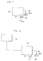
- Fig. 1 there is shown a plan view of a dicer 20.
- the dicer 20 includes a wafer supply part 22 which is able to receive a wafer case 24 conveyed from a previous manufacturing step.
- a wafer 24A is stored in the wafer case 24.
- a bar code reader 26 which is able to recognize a bar code 28A displayed on a card 28 to be described later only tracing the surface of the card 28.
- the card 28 is attached to the wafer case 24 and is then conveyed together with the wafer case 24.
- the dicer 20, as shown in Fig. 2 is connected to a controlling computer 30 and, in general, data necessary for the dicer 20 is previously registered in the controlling computer 30. However, data not registered in the controlling computer 30 is registered in a memory part of the dicer 20 and the registered data is set to be transmittable to the controlling computer 30.
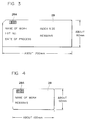
- a card 28 shown in Fig. 3 is formed in a so called mark sheet card size (having a length of about 200 mm, and a height of about 80 mm).
- a bar code 28A is displayed on the upper left portion of Fig. 3 by means of bonding, printing or similar means.
- the bar code 28A is set such that it has a given relation with respect to an ID number 12 (see Fig. 9) which is displayed on the wafer 10.
- the number of the bar code 28A is marked as a specific value on a carrier 24 for storing the wafer 24A therein and the bar code number is managed by means of the number of frames.
- a bar code number which is shown in Table 1 and corresponds to the kind of the wafer 24A, is marked on the carrier 24 and the marked data is managed by the controlling computer or the marked data is stored in a floppy disc, a memory card, a magnetic card or the like.
- the bar code number is registered in the card 28.
- the number of the bar code 28A may be set to be identical with the kind of the wafer 24A, as shown in Table 2.
- Table 2 Kinds of Wafers Bar Code Nos. T S K 0 0 1 T S K 0 0 1 T S K 1 0 0 T S K 1 0 0 : : : :
- a user's mark, a rod No., the date of processing, a wafer size and the like can be written into the remaining spaces of the card 28.
- a card 28 is formed in the shape of a so called telephone card size (having a length of about 100 mm, and a height of about 60 mm).
- a bar code 28A is displayed in the left end portion of the card 28 and a user's mark, an index, a wafer size and the like can be written into the remaining spaces of the card 28.
- a rod No. the date of processing and the like can be registered and the data registered in such magnetic portion can be rewritten.
- the processing data of the wafers are previously registered in a controlling computer 30 shown in Fig. 2 in such a manner that the wafer processing data correspond to the ID numbers of the wafers (that is, a relation shown in Table 1 or Table 2 is registered). And, as for the data not registered in the controlling computer 30, the data are previously registered in a memory part of the dicer 20 and such data are set to be transmittable to the controlling computer 30.
- a bar code writer (not shown) in a previous step to the dicer 20 is used to bond or print the bar code 28A at a given position of the card 28, the card 28 is attached to the wafer case 24, and the card 28 is delivered together with the wafer case 24.
- the wafer case 24 is delivered to a wafer supply part 22 of the dicer 20, then an operator takes off the card 28 attached to the wafer case 24 and the bar code reader 26 is contacted with the surface of the card 28 to thereby read out the bar code 28A.
- the bar code reader 26 reads out the bar code 28A and at the same time requests necessary data from the controlling computer 30 in accordance with the signal of the bar code 28A. Responsive to this, the necessary data is applied from the controlling computer 30 to the dicer 20 and the dicer 20, in accordance with the thus applied data, aligns the wafer 24A of the wafer case 24 by use of alignment means and then cuts the wafer 24A with the rotary edges thereof into a desired semiconductor chip.
- the controlling computer 30 is used to change the kinds of the wafers in the dicer 20, this is not limitative, but only the memory part of the dicer 20 can be used to carry out the wafer kind change.
- the bar code reader 26 calls out data, which corresponds to the bar code 28A read out, from the memory part of the dicer 20 and, responsive to the data called out, the dicer 20 is set to be operable (that is, the dicer 20 is switched to a state thereof suitable for machining of the wafer 24A). As a result of this, the wafer 24A can be aligned and diced.
- the bar code reader 26 of the dicer 20 is able to recognize the bar code 28A simply by touching the surface of the card 28 and is also able to output the thus recognized signal to the controlling computer 30 to call out the necessary data therefrom. Due to this, when the wafer 24A is diced by use of the dicer 20, there is eliminated the need for an operator to key input the data, thereby reducing the occurrences of troubles as well as enhancing the productivity of the wafers.
- the bar code reader 26 is inexpensive when compared with a recognizing device for recognizing the ID number, even if the bar code reader is provided in every wafer manufacturing step, it does not increase the cost of the wafer manufacturing line.
- the bar code 28A is registered as another embodiment for displaying the ID number.
- this is not limitative, but other display means such as a magnetic card or the like can also be employed, provided that it can be recognized easily.
- the bar code 28A is displayed on the card 28.
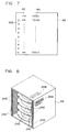
- a bar code 24B may be displayed on the wafer carrier 24.
- the operator uses the bar code reader 26 to read the bar code 24B.
- Fig. 5 is a view obtained by rewriting Fig. 8 into a plan view and the bar code 24B can be displayed on the upper surface, side surface or the like of the wafer carrier 24.
- 24E designates a groove into which the wafer 24 is mounted.
- the bar code is displayed on the card 28 or on the wafer case 24.
- other way of displaying is also possible.
- a bar code 42 and a name 44 of a wafer corresponding to the bar code 42 may be previously registered in a sheet of paper 40.
- an operator may bring the bar code reader 26 into contact with a bar code 42A corresponding to the wafer name (TS002) to read the bar code 42A, thereby switching the dicer 20.
Landscapes
- Dicing (AREA)
- Container, Conveyance, Adherence, Positioning, Of Wafer (AREA)
- Processing Of Stones Or Stones Resemblance Materials (AREA)
Applications Claiming Priority (2)
| Application Number | Priority Date | Filing Date | Title |
|---|---|---|---|
| JP332095/90 | 1990-11-29 | ||
| JP2332095A JPH04199733A (ja) | 1990-11-29 | 1990-11-29 | 半導体チップの製造方法及びその装置 |
Publications (2)
| Publication Number | Publication Date |
|---|---|
| EP0488053A1 true EP0488053A1 (de) | 1992-06-03 |
| EP0488053B1 EP0488053B1 (de) | 1996-07-17 |
Family
ID=18251089
Family Applications (1)
| Application Number | Title | Priority Date | Filing Date |
|---|---|---|---|
| EP91119860A Expired - Lifetime EP0488053B1 (de) | 1990-11-29 | 1991-11-21 | Methode zur Herstellung eines Halbleiterchips |
Country Status (3)
| Country | Link |
|---|---|
| EP (1) | EP0488053B1 (de) |
| JP (1) | JPH04199733A (de) |
| DE (1) | DE69120904T2 (de) |
Cited By (4)
| Publication number | Priority date | Publication date | Assignee | Title |
|---|---|---|---|---|
| EP0616364A4 (de) * | 1991-10-29 | 1994-08-01 | Komatsu Denshi Kinzoku Kk | Vorrichtung und verfahren zur herstellung von halbleiterscheiben. |
| WO1998052226A1 (en) * | 1997-05-15 | 1998-11-19 | Micron Technology, Inc. | Method and apparatus for identifying integrated circuits |
| US5956596A (en) * | 1995-11-06 | 1999-09-21 | Samsung Electronics Co., Ltd. | Method of forming and cleaning a laser marking region at a round zone of a semiconductor wafer |
| CN116475866A (zh) * | 2023-03-15 | 2023-07-25 | 河南仕佳光子科技股份有限公司 | 一种用于热光调制plc光芯片的磨抛方法 |
Families Citing this family (2)
| Publication number | Priority date | Publication date | Assignee | Title |
|---|---|---|---|---|
| JP2005101290A (ja) * | 2003-09-25 | 2005-04-14 | Disco Abrasive Syst Ltd | 半導体ウエーハの分割方法 |
| JP5134216B2 (ja) * | 2006-06-23 | 2013-01-30 | 株式会社ディスコ | ウエーハの加工結果管理方法 |
Citations (2)
| Publication number | Priority date | Publication date | Assignee | Title |
|---|---|---|---|---|
| EP0249762A1 (de) * | 1986-05-20 | 1987-12-23 | Fujitsu Limited | Identifizierung von Halbleiterscheiben mit Mustern des "Bar-code"-Typs |
| EP0132520B1 (de) * | 1983-06-23 | 1990-10-24 | International Business Machines Corporation | Verfahren zur Herstellung eines Halbleiterbauelementes |
Family Cites Families (4)
| Publication number | Priority date | Publication date | Assignee | Title |
|---|---|---|---|---|
| JPS6235637A (ja) * | 1985-08-09 | 1987-02-16 | Hitachi Ltd | ウエハ貼付装置 |
| JPS62128143A (ja) * | 1985-11-28 | 1987-06-10 | Nec Corp | 半導体基板カセツト |
| JPH0270403A (ja) * | 1988-09-06 | 1990-03-09 | Nec Corp | 全自動ウエハ切断機 |
| JPH02164016A (ja) * | 1988-12-19 | 1990-06-25 | Hitachi Ltd | ウエハ処理方法およびそれに用いるウエハ処理装置 |
-
1990
- 1990-11-29 JP JP2332095A patent/JPH04199733A/ja active Pending
-
1991
- 1991-11-21 EP EP91119860A patent/EP0488053B1/de not_active Expired - Lifetime
- 1991-11-21 DE DE69120904T patent/DE69120904T2/de not_active Expired - Fee Related
Patent Citations (2)
| Publication number | Priority date | Publication date | Assignee | Title |
|---|---|---|---|---|
| EP0132520B1 (de) * | 1983-06-23 | 1990-10-24 | International Business Machines Corporation | Verfahren zur Herstellung eines Halbleiterbauelementes |
| EP0249762A1 (de) * | 1986-05-20 | 1987-12-23 | Fujitsu Limited | Identifizierung von Halbleiterscheiben mit Mustern des "Bar-code"-Typs |
Non-Patent Citations (5)
| Title |
|---|
| PATENT ABSTRACTS OF JAPAN vol. 5, no. 171 (E-80)(843) 30 October 1981 & JP-A-56 100 454 ( MITSUBISHI DENKI K.K. ) * |
| PATENT ABSTRACTS OF JAPAN vol. 8, no. 49 (E-230)(1486) 6 March 1984 & JP-A-58 202 537 ( MITSUBISHI DENKI K.K. ) * |
| PATENT ABSTRACTS OF JAPAN vol. 9, no. 284 (E-357)(2007) 12 November 1985 & JP-A-60 124 952 ( FUJITSU K.K. ) * |
| RESEARCH DISCLOSURE. no. 285, January 1988, NEW YORK page 45; 'Tape Automated Bonding' Abstractnr.:28 557 * |
| SOLID STATE TECHNOLOGY. vol. 23, no. 7, July 1980, WASHINGTON US pages 54 - 55; G. DUNCAN: 'Proposed Alphanumeric Marking Standards for 125mm Silicon Wafers' * |
Cited By (7)
| Publication number | Priority date | Publication date | Assignee | Title |
|---|---|---|---|---|
| EP0616364A4 (de) * | 1991-10-29 | 1994-08-01 | Komatsu Denshi Kinzoku Kk | Vorrichtung und verfahren zur herstellung von halbleiterscheiben. |
| US5537325A (en) * | 1991-10-29 | 1996-07-16 | Komatsu Electronic Metals Co., Ltd. | Apparatus for and method of manufacturing semiconductor wafer |
| US5956596A (en) * | 1995-11-06 | 1999-09-21 | Samsung Electronics Co., Ltd. | Method of forming and cleaning a laser marking region at a round zone of a semiconductor wafer |
| WO1998052226A1 (en) * | 1997-05-15 | 1998-11-19 | Micron Technology, Inc. | Method and apparatus for identifying integrated circuits |
| US5984190A (en) * | 1997-05-15 | 1999-11-16 | Micron Technology, Inc. | Method and apparatus for identifying integrated circuits |
| USRE40623E1 (en) | 1997-05-15 | 2009-01-20 | Micron Technology, Inc. | Method and apparatus for identifying integrated circuits |
| CN116475866A (zh) * | 2023-03-15 | 2023-07-25 | 河南仕佳光子科技股份有限公司 | 一种用于热光调制plc光芯片的磨抛方法 |
Also Published As
| Publication number | Publication date |
|---|---|
| DE69120904D1 (de) | 1996-08-22 |
| DE69120904T2 (de) | 1996-11-28 |
| EP0488053B1 (de) | 1996-07-17 |
| JPH04199733A (ja) | 1992-07-20 |
Similar Documents
| Publication | Publication Date | Title |
|---|---|---|
| US5570293A (en) | Method and device for manufacturing a semiconductor chip | |
| KR102067294B1 (ko) | 반도체 장치의 제조 방법 | |
| KR101575831B1 (ko) | 개별 소자의 역방향 트레이서빌리티 및 반도체 디바이스의 순방향 트레이서빌리티 | |
| US7136721B2 (en) | Article management system and article management apparatus | |
| EP0488053A1 (de) | Methode zur Herstellung eines Halbleiterchips | |
| JPH05315207A (ja) | 半導体装置 | |
| JPH04146649A (ja) | 半導体チップの製造方法及びその装置 | |
| JPS61236136A (ja) | ウエハカセツト治具 | |
| JP2001091583A (ja) | 半導体チップを試験するためのシステム及びカセット | |
| JP6185492B2 (ja) | 個別部品後方追跡可能性および半導体装置前方追跡可能性 | |
| US4500080A (en) | Carrier for cleaning and etching wafers | |
| JPH09306873A (ja) | ウェーハの分割システム | |
| JP3639884B2 (ja) | ウエーハのダイシング方法 | |
| JP2584301B2 (ja) | 電子部品装着システム | |
| KR100228958B1 (ko) | 다이본딩 장치 | |
| JP4657585B2 (ja) | 半導体ウェーハの分割方法 | |
| JP7199766B1 (ja) | 生産設備におけるパーツ交換作業を支援するシステム、処理装置、および方法 | |
| JPS6357154A (ja) | 製品材料に関する工程デ−タの記録方法 | |
| JPH0760580A (ja) | Faシステム | |
| JP7692292B2 (ja) | 搬送トレイ及び搬送トレイの製造方法 | |
| JP6811411B2 (ja) | ダイシング装置 | |
| JPH01308042A (ja) | 半導体装置の製造方法 | |
| KR20250154233A (ko) | 와플 팩 추적 방법 및 그 장치 | |
| JPH03214743A (ja) | 半導体装置の製造システム | |
| JPH0682744B2 (ja) | 自動マスク搬送装置 |
Legal Events
| Date | Code | Title | Description |
|---|---|---|---|
| PUAI | Public reference made under article 153(3) epc to a published international application that has entered the european phase |
Free format text: ORIGINAL CODE: 0009012 |
|
| AK | Designated contracting states |
Kind code of ref document: A1 Designated state(s): DE FR GB IT |
|
| 17P | Request for examination filed |
Effective date: 19920703 |
|
| 17Q | First examination report despatched |
Effective date: 19940301 |
|
| GRAH | Despatch of communication of intention to grant a patent |
Free format text: ORIGINAL CODE: EPIDOS IGRA |
|
| GRAH | Despatch of communication of intention to grant a patent |
Free format text: ORIGINAL CODE: EPIDOS IGRA |
|
| GRAA | (expected) grant |
Free format text: ORIGINAL CODE: 0009210 |
|
| AK | Designated contracting states |
Kind code of ref document: B1 Designated state(s): DE FR GB IT |
|
| ITF | It: translation for a ep patent filed | ||
| REF | Corresponds to: |
Ref document number: 69120904 Country of ref document: DE Date of ref document: 19960822 |
|
| ET | Fr: translation filed | ||
| PLBE | No opposition filed within time limit |
Free format text: ORIGINAL CODE: 0009261 |
|
| STAA | Information on the status of an ep patent application or granted ep patent |
Free format text: STATUS: NO OPPOSITION FILED WITHIN TIME LIMIT |
|
| 26N | No opposition filed | ||
| REG | Reference to a national code |
Ref country code: GB Ref legal event code: IF02 |
|
| PGFP | Annual fee paid to national office [announced via postgrant information from national office to epo] |
Ref country code: GB Payment date: 20051118 Year of fee payment: 15 |
|
| PGFP | Annual fee paid to national office [announced via postgrant information from national office to epo] |
Ref country code: DE Payment date: 20051124 Year of fee payment: 15 |
|
| PGFP | Annual fee paid to national office [announced via postgrant information from national office to epo] |
Ref country code: FR Payment date: 20051128 Year of fee payment: 15 |
|
| REG | Reference to a national code |
Ref country code: GB Ref legal event code: 746 Effective date: 20051124 |
|
| PGFP | Annual fee paid to national office [announced via postgrant information from national office to epo] |
Ref country code: IT Payment date: 20061130 Year of fee payment: 16 |
|
| PG25 | Lapsed in a contracting state [announced via postgrant information from national office to epo] |
Ref country code: DE Free format text: LAPSE BECAUSE OF NON-PAYMENT OF DUE FEES Effective date: 20070601 |
|
| GBPC | Gb: european patent ceased through non-payment of renewal fee |
Effective date: 20061121 |
|
| REG | Reference to a national code |
Ref country code: FR Ref legal event code: ST Effective date: 20070731 |
|
| PG25 | Lapsed in a contracting state [announced via postgrant information from national office to epo] |
Ref country code: GB Free format text: LAPSE BECAUSE OF NON-PAYMENT OF DUE FEES Effective date: 20061121 |
|
| PG25 | Lapsed in a contracting state [announced via postgrant information from national office to epo] |
Ref country code: FR Free format text: LAPSE BECAUSE OF NON-PAYMENT OF DUE FEES Effective date: 20061130 |
|
| PG25 | Lapsed in a contracting state [announced via postgrant information from national office to epo] |
Ref country code: IT Free format text: LAPSE BECAUSE OF NON-PAYMENT OF DUE FEES Effective date: 20071121 |